國
國
國
國 立
立
立 交
立
交
交 通
交
通
通
通 大
大
大
大 學
學
學
學
電子工程學系
電子工程學系
電子工程學系
電子工程學系 電子研究所碩士班
電子研究所碩士班
電子研究所碩士班
電子研究所碩士班
碩士論文
碩士論文
碩士論文
碩士論文
低溫複晶矽薄膜電晶體
低溫複晶矽薄膜電晶體
低溫複晶矽薄膜電晶體
低溫複晶矽薄膜電晶體
其遷移率
其遷移率
其遷移率
其遷移率與可靠度之研究
與可靠度之研究
與可靠度之研究
與可靠度之研究
Study on the Mobility and Reliability of Low
Temperature Poly-Si Thin-Film Transistors
研 究 生:徐源竣
指導教授:雷添福 博士
低溫
低溫
低溫
低溫複晶矽薄膜電晶體之製程與可靠度之研究
複晶矽薄膜電晶體之製程與可靠度之研究
複晶矽薄膜電晶體之製程與可靠度之研究
複晶矽薄膜電晶體之製程與可靠度之研究
Study on the Mobility and Reliability of Low
Temperature Poly-Si Thin-Film Transistors
研 究 生:徐源竣 Student: Yuan-Jiun Hsu 指導教授:雷添福 博士 Advisor: Dr. Tan-Fu Lei
國
國
國
國 立
立
立
立 交
交
交
交 通
通
通
通 大
大
大 學
大
學
學
學
電子工程學系
電子工程學系
電子工程學系
電子工程學系 電子研究所碩士班
電子研究所碩士班
電子研究所碩士班
電子研究所碩士班
碩士論文
碩士論文
碩士論文
碩士論文
A ThesisSubmitted to Department of Electronics Engineering & Institute of Electronics College of Electrical Engineering
National Chiao Tung University In Partial Fulfillment of the Requirements
For the Degree of Master of Science
in
Electronic Engineering June 2006
Hsinchu Taiwan Republic of China
低溫
低溫
低溫
低溫複晶矽薄膜電晶體
複晶矽薄膜電晶體
複晶矽薄膜電晶體
複晶矽薄膜電晶體
之
之
之
之遷移率
遷移率
遷移率與可靠度之研究
遷移率
與可靠度之研究
與可靠度之研究
與可靠度之研究
學生
學生
學生
學生:
:
: 徐源竣
:
徐源竣
徐源竣
徐源竣
指導教授
指導教授:
指導教授
指導教授
:
: 雷添福
:
雷添福
雷添福 博士
雷添福
博士
博士
博士
國立交通大學
國立交通大學
國立交通大學
國立交通大學
電子工程學系
電子工程學系
電子工程學系
電子工程學系 電子研究所碩士班
電子研究所碩士班
電子研究所碩士班
電子研究所碩士班
摘
摘
摘
摘 要
要
要
要
在本論文中,首先,我們研究利用氮化矽層去覆蓋複晶矽薄膜電晶體的新 式結構。我們發現與傳統複晶矽薄膜電晶體相較之下,有著氮化矽覆蓋層的複晶 矽薄膜電晶體有較好的電特性。我們提高了導通電流及場效遷移率,這是因為氮 化矽覆蓋層在通道中造成張力還有降低源極/汲極的串聯電阻。再者,氮化矽覆 蓋層的複晶矽薄膜電晶體也抑制了扭曲效應 (Kink effect),閘極引發汲極漏電 (GIDL) , 還有改善了可靠度,這是因為此種新式結構薄膜電晶體可以降低橫向電 場。 接著,我們進行有關 P 型通道之多重通道(multi-channel)複晶矽薄膜電晶體 的研究。此種元件的電特性如導通電流,臨界電壓(threshold voltage)及次臨限擺 幅(subthreshold swing) 會隨著通道條數變多而被改善,這是因為我們提高了有效 的通道寬度和加強了閘極的控制能力。而元件的可靠度也會隨著通道條數增加而 被改善,這是因為在多重通道結構下加強了閘極的控制能力。 最後,我們探討有關複晶矽薄膜電晶體生命週期(lifetime)的問題。發現到最糟的熱載子應力測試條件跟元件的通道長度有相關性。在短通道元件中,最糟的 熱載子應力測試條件是閘極電壓等於臨界電壓而非傳統上閘極電壓等於二分之 一汲極電壓。此外,導通電流退化的情形在高和位的汲極應力測試下的不同的現 象。這是因為在薄膜電晶體中不僅碰撞游離(impact ionization)還有寄生雙極性接 面電晶體效應(parasitic bipolar junction transistor effect)去造成元件的退化。我們 亦發現當在粹取複晶矽薄膜電晶體之生命週期時與金屬氧化層場效電晶體有著 不同的現象,在一大範圍的汲極電壓應力測試下有著兩種斜率的生命週期投射現 象。
Study on the Mobility and Reliability of Low
Temperature Poly-Si Thin-Film Transistors
Student: Yuan-Jiun Hsu
Advisor: Dr. Tan-Fu Lei
Department of Electronics Engineering &
Institute of Electronics
National Chiao Tung University
ABSTRACT
In this thesis, first, we studied the new structure of poly-Si TFTs with capping silicon nitride passivation layer. It was found that this device have better electrical characteristic than convention poly-Si TFTs. We enhanced electron mobility and on current due to local tensile strain in the channel and low source/drain series resistance. Moreover, the proposed poly-Si TFTs also suppressed kink effect, effect of gate induced drain leakage (GIDL) and improved reliability due to low horizontal electric field in this new structure of poly-Si TFTs.
Then, p-channel poly-Si TFTs with multi-channel structure were studied. The device’s electrical characteristic such as on-current, threshold voltage, and subthreshold swing were improved with increasing the channel stripes due to the increasing effective channel width and enhancement of gate control capability. The reliability of proposed poly-Si TFTs were improved with increasing the stripes of channel. This is due to better gate control capability in multiple channel structure.
worst-case of stress condition depend on device channel length. In short channel device, the worst-case of stress condition is under VG≈Vth, not VG=1/2 VD. Moreover, Ion degradation under both high and low VD of stress conditions has different phenomena. This is due to not only impact ionization but also parasitic bipolar junction transistor effect to degradation poly-Si TFTs. Then, it is found that lifetime extraction of poly-Si TFTs is not the same with that of MOSFETs. There are dual slop lifetime projections in wide drain voltage.
誌謝
誌謝
誌謝
誌謝
首先向我的指導教授雷添福博士至上無限的謝意,在老師的細心指導下,本 論文得以順利完成。兩年的研究生涯中,不僅僅只是學習到做研究的精神與方 法,老師的關心、鼓勵與啟發,使我在面對將來漫長的人生旅途,受用無窮。 接下來,我要特別感謝謝明山學長,學長不僅在研究過程中都很熱心地幫助 我、指導我,在日常生活中也都特別的關心照顧我。另外要感謝已畢業的獻德學 長帶我進入薄膜電晶體這個領域,也要感謝郭柏儀學長在實驗上經驗的傳承,還 有小強學長、楊紹明學長、小賢學長、志仰學長、家文學長,感謝你們這些日子 以來的關心與指導。也要感謝伯浩、俊嘉、宗元、梓祥,你們這二年的陪伴、一 起修課、一起做實驗、一起玩樂,有了你們這二年的研究過程充實又快樂,也要 謝謝統億、錦石、仕傑、明爵、哲綸、文呈、久騰使得實驗室變的更熱鬧,懷念 與你們相處的日子,總之,謝謝實驗室裡的每個人,讓我過了這麼充實又快樂的 碩士班生涯。 最後,我要感謝我最親愛的家人,在我追學過程中一直的全力支持我,給我 最大的支持與鼓勵,在我失意與難過時,一直都是我最好的避風港,也要謝謝我 最可愛的女友,在這段時間內的支持與体諒,讓我更有動力去作研究。僅以此論 文獻予你們。Contents
Abstract (Chinese) ………I Abstract (English) ………..III Acknowledge ………V Contents ………..VI Table & Figure Captions .………...VIII
Chapter 1 Introduction ……….1
1.1 Overview of Poly-Si Thin-Film Transistors ....………...1
1.2 Motivation ……….………..……...3
1.3 Organization of the Thesis………..5
References ………7
Chapter 2 Performance Enhancement of Low Temperature Polysilicon Thin Film Transistor with Silicon Nitride Capping layer ………...………...13
2.1 Introduction ……….………...…..13
2.2 Device Fabrication ………...…………...………..14
2.3 Method of Device Parameter Extraction ………..…………15
2.3.1 Determination of Threshold Voltage ………...15
2.3.2 Determination of Subthreshold-Swing .………..….16
2.3.3 Determination of Field Effect Mobility..………...17
2.3.4 Determination of ON/OFF Current Ratio .……….….…....17
2.3.5 Extraction of Grain Boundary Trap State Density..……….……....18
2.4 Results and Discussion………...………..20
2.4.1 Characteristics of Poly-Si TFTs with capping silicon nitride layer.. …...20
2.5 Summary ……….……….…22
References ………..………23
Chapter 3 Characteristic and Reliability of P-Channel Poly-Si TFTs with Multi-Channel Structure……….………..37
3.1 Introduction ………..37
3.2 Experimental ………..………..38
3.3 Results and Discussion ……….39
3.3.1 Characteristics of P-Channel Poly-Si TFTs with Multiple Channels..…39
3.3.2 Reliability of P-Channel poly-Si TFTs with Multiple Channels...…...42
3.4 Summary ………...………...42
References ……….……….43
Chapter 4 Investigated the lifetime of low temperature poly-Si TFTs with different dimension of channel..………....58
4.1 Introducion ……….………..58
4.2 Experimental …...……….………59
4.3 Results and Discussion ……….60
4.4 Summary ...………...65
References ……..………66
TABLE CAPTIONS
Chapter 2
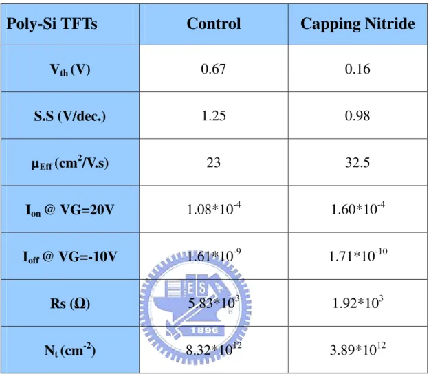
Table 2.1 Comparison of device characteristics of the Control and Capping Nitride poly-Si TFTs.
Chapter 3
Table 3-1 Summary of the dimensions of S1, M4, M8, M20 and M40 TFTs. All devices have the same active channel thickness 100nm, gate TEOS-oxide thickness 50nm, and total channel width 40µ m
Table 3-2 Summary of device parameters of the conventional and the proposed
p-channel multi-channel poly-Si TFTs (W/L = 40µ m/2µ m) with different stripes of channel.
FIGURE CAPTIONS
Chapter 2
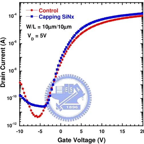
Fig. 2-1 Schematic diagram of fabrication process for Capping Nitride poly-Si TFTs Fig. 2-2 Transfer characteristics of the Control and Capping Nitride poly-Si TFTs
with VDS=5V
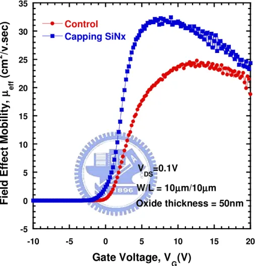
Fig. 2-3 Field-effect mobility of the Control and Capping Nitride poly-Si TFTs with VDS=0.1V
Fig. 2-4 Trap state density extraction of the Control and the Capping Nitride poly-Si TFTs
Fig. 2-5 Source/drain series resistance extraction of (a) the Control and (b) the Capping Nitride poly-Si TFTs
Fig. 2-6 Mechanism of reduction of source/drain series resistance
Fig. 2-7 Output characteristic of the Control and the Capping Nitride poly-Si TFTs Fig. 2-8 (a) on-current and (b) threshold voltage degradation as a function of stress
time under hot-carrier stress
Chapter 3
Fig. 3-1 Process flow of the conventional and multi-channel poly-Si TFTs.
Fig. 3-2 Cross-section of the conventional and multi-channel poly-Si TFTs is parallel to the direction of the source and drain electrode.
Fig. 3-3 Cross-section of the conventional and multi-channel poly-Si TFTs is perpendicular to the direction of the source and drain electrode.
Fig. 3-4 Top view of the conventional and multi-channel poly-Si TFTs in (a), (b), (c), and (d). (The effective channel width Weff = 40μm ; channel length L = 2 μm.)
Fig. 3-5 Transfer characteristics of the conventional and the proposed p-channel multi-channel poly-Si TFTs with different stripes of channel.
Fig. 3-6 Field effect mobility of the conventional and the proposed p-channel multi-channel poly-Si TFTs with different stripes of channel.
Fig. 3-7 Distribution of (a) Threshold voltage and (b) Field effect mobility of the proposed p-channel multi-channel poly-Si TFTs with different stripes of channel. The vertical bars indicate the minimum and maximum value of the devices characteristics and the squares are the average values
Fig. 3-8 Trap state density extraction of the conventional and the proposed p-channel multi-channel poly-Si TFTs with different stripes of channel. Fig. 3-9 Trap state density of the proposed multi-channel poly-Si TFTs with
different stripes of channel.
Fig. 3-10 Increasing ratio of the effective channel width and the on-state current as a function of number of channel stripes.
Fig. 3-11 Output characteristics of the conventional and the proposed p-channel poly-Si TFTs with different stripes of channel. (VG – Vth = 1; 2; 3V) Fig. 3-12 (a) on-current, and (b) threshold voltage degradation as a function of stress
time under hot-carrier stress.
Chapter 4
Fig. 4-1 Process flow of the conventional poly-Si TFTs. Fig. 4-2 Cross-section of the conventional poly-Si TFTs.
Fig. 4-3 Transfer characteristics of the conventional poly-Si TFTs
Fig. 4-4 On-current degradation under stress conditions of VG=1/2VD and VG=Vth at VDS=16V for different channel geometry
channel width of 10µ m
Fig. 4-6 Lifetime extraction of poly-Si TFTs with channel length of 2µ m and channel width of 10µ m
Fig. 4-7 Lifetime extraction of poly-Si TFTs with channel length of 2µ m and channel width of 2µ m
Fig. 4-8 Schematical plot of the occurrence of impact ionization and bipolar multiplication in the poly-Si TFTs.
Chapter 1
Introduction
1.1
Overview of Low Temperature Poly-Si Thin-Film Transistors
The study of polycrystalline silicon (poly-Si) thin film transistors (TFTs) fabricated using a maximum temperature below 600C commenced in 1980s. We defined this kind of poly-Si TFTs as Low temperature polysilicon thin film transistors (LTPS-TFTs) . It have received much attention in recent years because of their applications , such as active matrix liquid crystal displays (AMLCDs) [1-3] , active matrix organic light emitting displays (AMOLEDs) [4-6] , high density static random access memories (SRAMs) [7], electrical erasable programming read only memories (EEPROM) [8][9] and candidate for 3-dimenstion ICs’ applications [10] . Within those applications, the application of active matrix liquid crystal displays (AMLCDs) is the major driving force to promote the developments of poly-Si TFT technology .
The first generation of active matrix liquid crystal displays (AMLCDs) used a-Si:H TFTs for the pixel switching device. The advantages of a-Si:H TFTs are their compatibility with low processing temperature on large-area glass substrates and low leakage current due to the high off-stated impedance. However , the low electron field-effect mobility(<1 cm2/Vs) has limited the development of AMLCDs technology. So , the poly-Si TFTs acted important role for AMLCDs development , because the high field effect mobility and the high driving current of poly-Si TFTs makes the integration of switching pixels and driver circuits possible [11]. Moreover, the aperture ratio and the panel brightness can be also greatly promoted due to small
device size needed using poly-Si TFTs [12]. Therefore, the performance of display can be significantly improved. As a result, ploy-Si TFTs have a great potential to realized high-performance large-area AMLCDs applications, and further to accomplish System-on-Panel (SOP).
As compared with single crystalline silicon, the polycrystalline Silicon may consist of many grains, whose boundaries are composed of unsatisfied dangling silicon bonds that may trap charge carriers and become charged. This results in the formation of potential barriers between grains and also between the grain interior and its boundary [13]. The major effect of grain boundaries and intra-grain defects on the electrical performance of a TFT results from lowering the carrier mobility. This results in a degradation of drive current and subthreshold swing , and increases the threshold voltage, leakage current, and the temperature dependence of the device[13][14]. In order to obtain desirable electrical characteristics of poly-Si TFTs , several methods have been proposed to improve the device performance by enlarging the grain size of poly-Si films[15][16] and reducing the trap states in grain boundaries . Many crystallization techniques have been proposed to achieve low temperature polycrystalline silicon (LTPS) TFTs , such as SPC (solid phase crystallization)[17] , ELA (excimer laser annealing)[18][19] and MILC (metal induced lateral crystallization)[20]. Plasma treatments is also a method for reducing trap states in grain boundaries, various plasmas such as H2 [21], NH3 [22], N2O[23] and O2 plasmas [24] have been intensely investigated in recent years.
Moreover, the device performance could also be improved by adopting novel device structures. Offset drain/source [25], Lightly doped drain (LDD) [26], gate overlapped LDD [27] , multiple channel structure [28] , Double or multiple gate structures [29], vertical channel [30] have been proposed and investigated intensively.
1.2
Motivation
In this thesis, we focus on the enhancement of mobility of poly-Si TFTs. This is because we want to gain higher on-current for AMLCD applications. Thus, the aperture ratio will be increased and then brightness will certainly increase. In recent years, the poly-Si TFTs have many applications which not only AMLCD but also 3-d circuit applications are very popular. We enhanced mobility of poly-Si TFTs can help system and circuit designer having wide window to design.
First, we have proposed that using nitride capping layer enhances mobility. It have been demonstrated that tensile strain in the channel will enhance electron mobility. Previous reports indicated that they applied mechanical stress on the wafer to test device and then observed electrical characteristics of tested device. It was found that tensile strain improves the electron mobility and the drain current of n-channel device including MOSFETs and TFTs [31][32]. On the contrary, Compressive strain reduced the electron mobility. It is well know that nitride layer has tensile stress. So, we want to utilize tensile strain of silicon nitride layer to forming compressively strained polysilicon gate electrode and then give a tensile stress on the channel [33]. Moreover, in mainstream CMOS technology, nitride spacer was used for reducing off-state leakage and improving the on-state drivability [34]. Because nitride spacer can induce electron to reduce resistance in offset region for improving the on-state drivability. Furthermore, the capping silicon nitride layer can reduce moisture incorporation. So, we proposed poly-Si TFTs with capping nitride layer to improve device performance.
Then, we proposed the p-channel poly-Si TFTs with multichannel structure. P-channel poly-Si TFTs have been used for many applications, such as low-power SRAMs [35], High-Resolution Active Matrix [36] and EEPROM’s [37]. In circuit
design, CMOS technique is a very important technique. Because it have many advantage such as low power consumption, fully restored logic and better reliability. We would like realized CMOS technique by using TFTs device. So P-Channel and N-Channel TFTs are needed for integrated CMOS circuit. Moreover, the stability of p-channel polysilicon TFTs has not been investigated as much as n-channel polysilicon TFTs. So, we will discuss characteristic and reliability of P-Channel poly-Si TFTs in this thesis. It is well know that the characteristics of poly-Si TFTs are dominated by the large trap density in poly-Si film. When channel width scaled down, devices are reported to exhibit better performance such as lower threshold voltage and smaller trap density [38]-[40]. As a result, Poly-Si TFTs with narrow and multiple channels have been proposed to improve device performance [41][42]. Previous reports indicated that the existence regions near the poly-Si pattern edge where the grain boundary trap density is much smaller than elsewhere in the poly-Si film [38]. When channel width decreasing the effect of poly-Si pattern edge dominates and causes an effective trap density decreasing. Moreover, Due to the formation of active region island the gate electrode layer that climbs across the channel may induce side channels in both sides of the channel region. When channel width scaled down these side-channels become comparable to the main channel, accordingly increasing the effective channel width. Additionally, in CMOS technology, tri-gate [43] structure has been reported to exhibit superior gate control over the channel than a conventional single-gate MOSFET. Thus, we incorporate multi-channel with different channel widths, and tri-gate structure to achieve the high-performance and high reliability poly-Si TFTs. So, we proposed p-channel multichannel poly-Si TFTs and discussed characteristics and reliability of proposed poly-Si TFTs.
Finally, we focus on the reliability of poly-Si TFTs. It has been reported that the worst-case hot carrier degradation for conventional MOSFETs is under VG=1/2 VD
[44], and the device’s degradation depends on the trap states generation, which are proportional to the Isub [45]. This means that drain-avalanche-hot-carrier (DAHC) injection causes the severest damage on the device’s characteristics. Therefore, DAHC-induced substrate current Isub was used to monitor the device degradation and predict the device lifetime. However, it is known that the worst-case hot carrier degradation for SOI MOSFETs is under VG≈Vth [46]. After hot-carrier stress, the degradation mechanism of the device was significantly different at both low and high drain bias [47][48]. They concluded that the parasitic bipolar transistors (PBT) might be the dominate factor to enhance the stressed current and also the device degradation rate. So, the lifetime of MOSFETs is unsuitable for SOI MOSFETs.
Poly-Si TFTs have received much attention in recent years because of their applications. Although, it have many studies to improve performance of poly-Si TFTs. However, the lifetime issues of poly-Si TFTs are not well studied. Because body contact is a lack of poly-Si TFTs, the floating body effect will influence the reliability of device. To date, there still does not exit a clear consensus on the hot-carrier effect of these devices compared to bulk. Therefore, in this thesis, we want to investigate the lifetime prediction of poly-Si TFTs, and the degradation mechanism at different drain bias under hot carrier stress.
1.3
Organization of the Thesis
In the following sections, we will show our research efforts.
In Chapter 2, the electrical characteristics and fabrication processes of low temperature poly-Si TFTs with silicon nitride capping layer will be proposed. Experimental results reveal that the performance and reliability of our devices have remarkable improvements in comparison with conventional TFTs. Additionally, we
make a detail discussion to explain the results of experimental.
In Chapter 3, the fabrication processes and electrical characteristics of p-channel ploy-Si TFTs with different stripes of channel will be proposed. Experimental results reveal that poly-Si TFTs with multiple channels have better performance and reliability than the conventional TFTs. Then, we will make a complete discussion about the electrical characteristics and reliability issue of poly-Si TFTs with multiple channels.
In Chapter 4, the reliability issue of poly-Si TFTs with different channel geometry will be investigated by applying different drain bias. It is found that Ion degradation under both high and low drain bias of stress conditions has different phenomenon. Then, we will analyze the degradation mechanism under hot carrier stress with wide drain voltage bias for the devices with different channel geometry.
References:
[1] Y. Oana, “Current and future technology of low-temperature poly-Si TFT-LCDs,”
Journal of the SID, vol. 9, pp. 169-172, 2001.
[2] S. Morozumi, K. Oguchi, S. Yazawa, Y. Kodaira, H. Ohshima, and T. Mano, “B/W and color LC video display addressed by poly-Si TFTs,” SID Dig., pp.156, 1983. [3] R. E. Proano, R. S. Misage, D. Jones, and D. G. Ast, “Guest-host active matrix
liquid-crystal display using high-voltage polysilicon thin film transistors,” IEEE
Trans. Electron Devices, vol. 38, pp. 1781, 1991.
[4] Mark Stewart, Robert S. Howell , Leo Pires, Miltiadis K. Hatalis, Webster Howard, and Olivier Prache, “Polysilicon VGA active matrix OLED displays – technology and performance”, in IEDM tech, Dig., 1998,pp.871-874
[5] Mark Stewart, Robert S. Howell , Leo Pires, Miltiadis K. Hatalis, “Polysilicon TFT technology for active matrix OLED displays,” IEEE Trans. Electron Devices, vol. 48,pp.845-851,2001.
[6] Zhiguo Meng and Man Wong, “Active-matrix organic light-emitting diode displays realized using metal-induced unilaterally crystallized polycrystalline silicon thin-film transistors,” IEEE Trans. Electron Devices, vol.49,pp. 991-996,2002.
[7] S. Batra, “Development of drain-offset (DO) TFT technology for high density SRAM’s,” Extended Abstracts, vol.94-2, in Electrochemical Soc. Fall Mtg.,
Miami Beach, FL, Oct. pp. 677,1994.
[8] M. Cao, et al., “A simple EEPROM cell using twin polysilicon thin-film transistors,” IEEE Trans. Electron Devices, vol. 15, pp. 304, 1994.
[9] N. D. Young, G. Harkin, R. M. Bunn, D. J. McCulloch, and I. D. French, “The fabrication and characterization of EEPROM arrays on glass using a low
temperature poly-Si TFT process,” IEEE Trans. Electron Devices, vol. 43, pp. 1930-1936, 1996.
[10] K. Banerjee, S. J. Souri, P. Kapur, and K. C. Saraswat, “3-D ICs: a novel chip design for improving deep-submicrometer interconnect performance and system-on-chip integration,” Proceedings of the IEEE, vol.89, pp. 602-633, 2001.
[11] W. G. Hawkins, “Polycrystalline-Silicon device technology for large-area electronics,” IEEE Trans, Electron Devices, vol. 33, pp. 477-481, 1986
[12] I. –W. Wu, “Cell design considerations for high-aperture-ratio direct-view and projection polysilicon TFT-LCDs,” in SID Tech. Dig., pp. 19, 1995.
[13] S. D. S. Malhi, H. Shichijo, S. K. Vanerjee, R. Sundaresan, M. Elahy, G. P. Pollack, W. F. Richardson, A. H. Shah, L. R. Hite, R. H. Womack, P. K. Chatterjee, and H. W. Lam, IEEE Trans. Electron Devices, vol. 32, pp. 258, 1985.
[14] T. I. Kamins, Polycrystalline Silicon for Integrated Circuit Applications (Kluwer, Norwell, MA, 1988).
[15] C. H, Hong, C. Y. Park and H. J. Kim, “Structure and crystallization of low pressure chemical vapor deposited silicon films using Si2H2 gas,” J. Appl.
Phys., vol. 71, pp. 5427-5432, 1992.
[16] J. H. Jeon, M. C. Lee, K. C. Park, M. K. Han, “A new polycrystalline silicon TFT with a single grain boundary in the channel,” IEEE Electron Device Lett. Vol. 22, no. 9, pp. 429-431, 2001
[17] A. Nakamura, F. Emoto, E. Fujii, and A. Tamamoto, “A high-reliability, low-operation-voltage monolithic active-matrix LCD by using advanced solid-phase growth technique,” IEDM Tech. pp.847, 1990.
thin-film transistors,” IEEE Electron Device Lett., vol. 20, no. 2, pp. 77-79, Feb. 1999.
[19] N. Kudo, N. Kusumoto, T. Inushima, and S. Yamazaki, “Characterization of polycrystalline-Si thin-film transistors fabricated by excimer laser annealing method,” IEEE Trans. Electron Devices, vol. 40, pp. 1876-1879, Oct. 1994.
[20] S. W. Lee, T. H. Ihn, and S. K. Joo, “Fabrication of high-mobility p-channel poly-Si thin-film transistors by self-aligned metal-induced lateral crystallization,”
IEEE Electron Device Lett., vol. 17, no. 8, pp. 407-409, Aug. 1996.
[21] A. Yin, and S. J. Fonash, “High-performance p-channel poly-Si TFT’s using electron cyclotron resonance hydrogen plasma passivation,” IEEE Electron Device lett., vol.15, no. 12, pp. 502-503, 1994.
[22] C. K. Yang, T. F. Lei, C. L. Lee, “The combined effects of low pressure NH3 annealing and H2 plasma hydrogenation on polysilicon thin-film-transistors,”
IEEE Electron Device lett., vol. 15, pp. 389-390, 1994.
[23] J. W. Lee, N. I. Lee, J. I. Kan, C. H. Han, “Characteristics of polysilicon thin-film transistor with thin-gate dielectric grown by electron cyclotron resonance nitrous oxide plasma,” IEEE Electron Device lett., vol. 18, pp. 172-174, 1997.
[24] K. C. Moon, J. H. Lee, M. K. Han, “Improvement of polycrystalline silicon thin film transistor using oxygen plasma pretreatment before laser crystallization,”
IEEE Trans. Electron Devices, vol. 49, pp. 1319-1322, 2002.
[25] B. H. Min, C. M. Park and M. K. Han, “A novel offset gated polysilicon thin film transistor without and additional offset mask,” IEEE Electron Device lett., vol. 16, no. 5, pp. 161-163, 1995.
[26] P. S. Shih, C. Y. Chang, T. C. Chang, T. Y. Huang, D. Z. Peng and C. F. Yeh, “A novel lightly doped drain polysilicon thin-film transistor with oxide sidewall spacer formed by one-step selective liquid phase deposition,” IEEE Electron
Device lett., vol. 20, no. 8, pp.421-423, 1999.
[27] K. Y. Choi and M. K. Han, “A novel gate-overlapped LDD poly-Si thin-film transistor,” IEEE Electron Device lett., vol. 17, no. 12, pp. 566-568, 1996.
[28] T. Unagami and O. Kogure, “Large on/off current ratio and low leakage current poly-Si TFTs with multichannel structure,” IEEE Trans. Electron Devices, vol.35, no. 11, pp. 1986-1989, 1988.
[29] T. Y. Huang, A. G. Lewis, I. W. Wu, A. Chiang, and R. H. Bruce, “New intra gate offset high voltage thin film transistor with misalignment immunity,” Electronics
lett., vol. 25, no. 8, pp. 544-545, 1989.
[30] C. S. Lai, C. L. Lee, T. F. Lei and H. N. Chern, “A novel vertical bottom-gate polysilicon thin film transistor with self-aligned offset,” IEEE Electron Device lett., vol. 17, no. 5, pp. 199-201, 1996.
[31] S. Maikap, C.-Y. Yu, S.-R. Jan, M. H. Lee, and C. W. Liu, “Mechanically Strained Strained-Si NMOSFETs,” IEEE Electron Device Lett., vol. 25, no. 1 pp. 40–42, 2004.
[32] Pai-hui Iris Hsu , M. Huang, H. Gleskova, Z. Xi, Z. Suo, S. Wagner, and James C. Sturm, “Effects of Mechanical Strain on TFTs on Spherical Domes” IEEE Trans.
Electron Devices, vol. 51, no. 3, pp. 371-377, 2004
[33] Tsung Yi Lu and Tien Sheng Chao, “Mobility Enhancement in Local Strain Channel nMOSFETs by Stacked a-Si/Poly-Si Gate and Capping Nitride,” IEEE
Electron Device Lett., vol. 26, no. 4 pp. 267–269, 2005.
[34]R. Tsuchiya, K. Ohnishi, M. Horiuchi, S. Tsujikawa, Y. Shimamoto, N. Inada, J. Yugami, F. Ootsuka, and T. Onai, “Femto-second CMOS technology with high-k offset spacer and SiN gate dielectric with oxygen-enriched interface,” in VLSI
Tech. Symp. Dig., HI, 2002, pp. 150–151.
[35] H. Kuriyama, Y. Ishigaki, Y. Fujii, S. Maegawa, S. Maeda, S. Miyamoto, K. Tsutsumi, and H. Miyoshi, “A C-Switch Cell for Low-Voltage Operation and
High-Density SRAMs,” in IEDM Tech. Dig., pp. 279-282, 1996.
[36] A. Mimura, J. I. Ohwada, Y. Hosokawa, T. Suzuki, H. Kawakami, and K. Miyata, “A High-Resolution Active Matrix Using p-Channel SO1 TFT’s,” IEEE Trans.
Electron Devices, vol. 35, no. 4, pp. 418-425, 1988.
[37] Nae-In Lee, Jin-Woo Lee, Hyoung-Sub Kim, and Chul-Hi Han, “High-Performance EEPROM’s Using N- and P-Channel Polysilicon Thin-Film Transistors with Electron Cyclotron Resonance N O-Plasma Oxide”
IEEE Electron Device Lett., Vol. 20, no. 1, pp. 15-17, 1999.
[38] N. Yamauchi, J-J. J. Hajjar, Rafael Reif, Kenji Nakazawa, and Keiji Tanaka, “Characteristics of narrow-channel polysilicon thin-film transistors,” IEEE Trans.
Electron Devices, vol. 38, no. 11, pp. 1967-1968, 1991.
[39] D. N. Yaung, Y. K. Fang, K. C. Hwang, K. Y. Lee, K. H. Wu, J. J. Ho, C. Y. Chen, Y. J. Wang, M. S. Liang, J. Y. Lee, and S. G. Wuu, “Narrow width effects of bottom-gate polysilicon thin film transistors,” IEEE Electron Device Lett., vol. 19, PP, 429-431, 1988.
[40] H. W. Zan, T. C. Chang, P. S. Shih, D. Z. Peng, T. Y. Huang, and C. Y. Chang, “Analysis of Narrow Width Effects in polycrystalline Silicon Thin Film Transistors,” Jpn. J. Appl. Phys., vol. 42, part 1, no. 1, pp. 28-32, 2003.
[41] T. Unagami, “High-voltage poly-Si TFT’s with multichannel structure,” IEEE
Trans. Electron Devices, vol. 35, no. 12, pp. 2363-2367, 1991.
[42] T. Takeshita, T. Unagami, and O. Kogure, “Study on narrow-strip polycrystalline silicon thin film transistors,” J. Appl. Phys., vol. 27, no. 10, pp. 1937-1941, 1988. [43] B. S. Doyle, S. Datta, M. Doczy, S. Hareland, B. Jin, J. Kavalieros, T. Linton, A. Murthy, R. Rios, and R. Chau, “High Performance Fully-Depleted Tri-Gate CMOS Transistors,” IEEE Electron Device Lett., vol. 24, no. 4, PP. 263-265, 2003.
[44] P. H. Worelee, C. Juffermans, H. Lifka, W. Manders, F. M. Oude Lansink, G. M. Paulzen, P. Sheridan, and A. Walker, “A half-micron CMOS technology using ultra-thin silicon on insulator,” in IEDM Tech. Dig., pp. 583-586, 1990.
[45] C. M. Hu, S. C. Tam, F. C. Hsu, P. K. Ko, T. Y. Chan, and K. W. Terrill, “Hot electron induced MOSFET degradation—model, monitor, and improvement,”
IEEE Trans. Electron Devices, vol. 32, no. 2, pp. 375-385, 1985.
[46] L. T. Su, H. Fang, J. E. Chung, and D. A. Antoniadis, “Hot-carrier effects in fully-depleted SOI nMOSFETs,” in IEDM Tech. Dig., pp. 349-352, 1992.
[47] J. W. Ratkovic, W. M. Huang, B. Y. Hwang, M. Racanelli, J. Forestner, and J. Woo, “Novel device lifetime behavior and hot-carrier degradation mechanisms under VGS≈VTH stress for thin-film SOI nMOSFETs,” in IEDM Tech. Dig., pp. 639-642, 1995.
[48] J. W. Ratkovic, W. M. Huang, B. Y. Hwang, M. Racanelli, J. Forestner, and J. Woo, “Lifetime reliability of thin-film SOI nMOSFET’s,” IEEE Electron Device
Chapter 2
Performance Enhancement of Low Temperature
Polysilicon Thin Film Transistor with Silicon Nitride
Capping layer
2.1
Introduction
In recent years, flexible electronics have been investigated and were paid attention, such as electronic paper, flexible display, sensor skin and electrotextiles. It required building electron device on flexible and deformable substrate [1]-[4]. Therefore, device will be stressed when operating flexible electronics. In this condition, mechanical strain is a major force to stress device.
There are many researches to comprehend effect of mechanical strain in device. In previous reported, they measured device characteristic when device under mechanical strain. it was found that tensile strain improves the electron mobility and the drain current of n-channel device including MOSFETs and TFTs [5][6]. On the contrary, Compressive strain reduced the electron mobility.
Recently, the strain-Si MOSFETs have become attractive for high speed complementary-metal-oxide-semiconductor (CMOS) device applications [7][8].the improvement of carrier mobility has been intensely studied by introducing strain in the channel region, such as strained-Si on SiGe substrate. However, the fabrication of the strained-Si devices is more complicated, such as forming a relaxed SiGe buffer layer. Previously studied indicated that uniaxial strained channel from contact etch stop silicon nitride (SiN) layer increase current drivability[9][10]. Because silicon
nitride layer has tensile strain and further forming compressively strained polysilicon gate electrode and then give a tensile stress on the channel.
In this chapter, we fabricated poly-Si TFTs with capping silicon nitride layer to created a tensile stress on the channel. It was found that this device have better electrical characteristic than convention poly-Si TFTs. We enhanced electron mobility and on current due to local tensile strain and low source/drain series resistance and then suppressed kink effect, gate induced drain leakage(GIDL) effect and improved reliability due to low horizontal electric field in Capping Nitride poly-Si TFTs. We will make a detail discussion in later section.
2.2
Device Fabrication
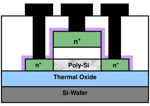
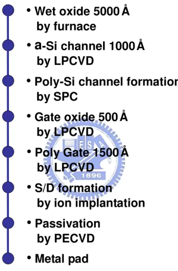
Figure 2-1 show the process flow and cross-sectional view of the investigated poly-Si TFT. First, 500-nm-thick thermal oxide was grown on the Si wafer by using a furnace system. All the experimental devices in this study were fabricated on thermally oxidized Si wafers. Then, 50-nm-thick amorphous silicon layers were deposited on the thermal oxide layer using a low-pressure chemical vapor deposition (LPCVD) system at 550°C. Then, amorphous silicon films were recrystallized by solid phase crystallization (SPC) method at 600°C for 24 hours in an N2 ambient to form poly-Si films. Poly-Si films were patterned into active regions by transformer couple plasma (TCP) etching system using mixture gases of Cl2 and HBr.
After RCA cleaning procedure, a 50-nm-thick TEOS oxide was deposited by LPCVD with TEOS and O2 gases at 695°C to form the gate insulator. A 150-nm-thick poly-Si was deposited to serve as the gate electrode by LPCVD at 595°C. Then, the poly-Si film was patterned and etched by TCP etching system to form the gate electrode and the gate oxide on source/drain was removed using dilute HF solution. The regions of source, drain, and gate were doped by a self-aligned phosphorous ion
implantation at the dosage and energy of 5×10¹⁵ions/cm-2 and 20keV, respectively. The dopant activation was performed by furnace system at 600°C for 12 hours, followed by a deposition of 250nm-thick silicon nitride layer and 300nm-thick passivation oxide using PECVD system at 350°C and the definition of contact holes. Then, weetched passivation oxide by BOE solution. After removed passivation oxide, 90% silicon nitride layer was etched by dry etching system and utilized oxide layer as a hard mask for etching 10% silicon nitride layer by wet etch in H3PO4 solution. Finally, a 800-nm-thick Al was deposited by sputter and patterned for metal pads, and devices were passivated by NH3 plasma treatment for 30 minute at 300°C. For comparison, the control samples have no capping nitride layer. It only deposited passivaton oxide using PECVD system at 350°C.
2.3
Method of Device Parameter Extraction
In this thesis, we use Ellipsometer to measure the thickness of poly-Si, amorphous-Si and TEOS oxide films in the fabrication procedure. All the electrical characteristics of proposed poly-Si TFTs were measured by HP 4156B-Precision Semiconductor Parameter Analyzer.
Many methods have been proposed to extract the characteristic parameters of poly-Si TFTs. In this section, those methods are described.
2.3.1
Determination of Threshold Voltage
Threshold voltage (Vth) is an important parameter required for the channel length-width and series resistance measurements. However, Vth is not uniquely defined. Various definitions have been proposed and the reason can be found in ID-VGS curves. One of the most common techniques is the linear extrapolation method with the drain current measured as a function of gate voltage at a low drain voltage of
50~100mV to ensure operation in the linear region [17]. The drain current is not zero when VGS below threshold voltage and approaches zero asymptotically. Hence the IDS versus VGS curve can be extrapolated to ID=0, and the Vth is determined from the extrapolated intercept of gate voltage (VGS) by
2 DS GS th V V V = − --- (Eq. 2.1) Equation (2.1) is strictly only valid for negligible series resistance. Fortunately series resistance is usually negligible at the low drain current when threshold voltage measurements are made. The IDS-VGS curve deviates from a straight line at gate voltage below Vth due to subthreshold current and above Vth due to series resistance and mobility degradation effects. It is common practice to find the point of maximum slope of the IDS-VGS curve and fit a straight line to extrapolate to ID=0 by means of finding the point of maximum of transconductance (Gm).
In this thesis, we use a simpler method to determinate the Vth called constant drain current method. The voltage at a specified threshold drain current is taken as the Vth. This method is adopted in the most studied papers of poly-Si TFTs. It can be given a threshold voltage close to that obtained by the complex linear extrapolation method. Typically, the threshold current is specified at (W/L)×10nA for VDS=0.1V and (W/L)×100nA for VDS=5V, where W and L are channel width and channel length, respectively.
2.3.2
Determination of Subthreshold-Swing
Subthreshold swing (S.S.) is a typical parameter to describe the control ability of gate toward channel, which reflects the turn on/off speed of a device. It is defined as the amount of gate voltage required to increase/decrease drain current by one order of magnitude.
The S.S. should be independent of drain voltage and gate voltage. However, in reality, the S.S. increases with drain voltage due to channel shortening effect such as charge sharing, avalanche multiplication and punchthrough effect. The subthreshold swing is also related to gate voltage due to undesirable and inevitable factors such as the serial resistance and interface states.
In this thesis, the S.S. is defined as one-third of the gate voltage required to decrease the threshold current by three orders of magnitude. The threshold current is specified to be the drain current when the gate voltage is equal to threshold voltage.
2.3.3
Determination of Field Effect Mobility
Usually, field effect mobility (µeff) is determined from the maximum value of transconductance (Gm) at low drain bias. The transfer characteristics of poly-Si TFTs are similar to those of conventional MOSFETs, so that the first order of I-V relation in the bulk Si MOSFETs can be applied to poly-Si TFTs. The drain current in linear region (VDS<VGS-Vth) can be approximated as the following equation:
(
)
− − = 2 2 1 DS DS th GS ox eff DS V V V V L W C Iµ
--- (Eq. 2.2)where W and L are channel width and channel length, respectively. Cox is the gate
oxide capacitance per unit area and Vth is the threshold voltage. Thus, the
transconductance is given by DS ox eff GS DS m V L W C V I g = ∂ ∂ =
µ
--- (Eq. 2.3)Therefore, the field-effect mobility is
(max) →0 = m VDS DS ox eff g WV C L
µ
--- (Eq.2.4)On/off current ratio is one of the most important parameters of poly-Si TFTs since a high-performance device exhibits not only a large on-current but also a small off-current (leakage current). The leakage current mechanism in poly-Si TFTs is not like that in MOSFET. In MOSFET, the channel is composed of single crystalline Si and the leakage current is due to the tunneling of minority carrier from drain region to accumulation layer located in channel region. However, in poly-Si TFTs, the channel is composed of poly-Si. A large amount of trap state densities in grain structure attribute a lot of defect states in energy band gap to enhance the tunneling effect. Therefore, the leakage current is much larger in poly-Si TFTs than in MOSFET. When the voltage drops between gate voltage and drain voltage increases, the band gap width decreases and the tunneling effect becomes much more severe. Normally we can find this effect in typical poly-Si TFTs’ IDS-VGS characteristics where the magnitude of leakage current will reach a minimum and then increase as the gate voltage decreases/increases for n/p-channel TFTs.
There are a lot of ways to specify the on and off-current. In this chapter, take n-channel poly-Si TFTs for examples, the on-current is defined as the drain current when gate voltage at the maximum value and drain voltage is 5V. The off-current is specified as the minimum current when drain voltage equals to 5V.
V V at Plot V I of Current Minimum V V at Plot V I of Current Maximum I I DS GS DS DS GS DS OFF ON 5 5 = − = − = --- (Eq. 2.5)
2.3.5
Extraction of Grain Boundary Trap State Density
The Trap State Density (Nt), which can be determined by the theory established by Levinson et al. [18], which is based on Seto’s theory [19].
− = GS ox Si c t GS DS ox FE DS V kTC L N q V V L W C I
ε
µ
8 exp 2 3 --- (Eq. 2.6) Where,µeff field-effect mobility of carriers
q electron charge
k Boltzmann’s constant
εSi dielectric constant of silicon
T temperature
Nt trap-state density per unit area
Lc channel thickness
This expression, first developed by Levinson et al., is a standard MOSFET’s equation with an activated mobility, which depends on the grain-boundary barrier height. Levinson et al. assumed that the channel thickness was constant and equal to the thickness of the poly-Si film (t). This simplifying assumption is permissible only for very thin film (t<10nm). The trap-state density can be obtained by extracting a straight line on the plot of ln(IDS/VGS) versus 1/VGS at low drain voltage and high gate voltage.
Proano et al. [20] thought that a barrier approximation is to calculate the gate induced carrier channel thickness by solving Poisson’s equation for an undoped material and to define the channel thickness (Lc) as a thickness in which 80% of the total charges were induced by the gate. Doing so, one obtains
(
GS fb)
SiO Si ox c V V q kTt L − = 2 8ε
ε
--- (Eq. 2.7)which varies inversely with (VGS−Vfb). This predicts, by substituting Eq.2.7 into
Eq.2.6, that ln[IDS/(VGS−Vfb)] versus 1/(VGS−Vfb) 2
. We use the gate voltage at which minimum leakage current occurs as flat-band voltage (Vfb). Effective trap-state
2.4
Results and Discussion
2.4.1
Characteristics of poly-Si TFTs with capping silicon nitride layer
We measured device characteristics while we have done the device fabrication. Fig. 2-2 shows the transfer characteristics (IDS-VGS) for the control and Capping Nitride poly-Si TFTs. The measurements was performed at drain voltage of VDS=5V. The measured and extracted parameters from the devices are listed in table 2-1. the threshold voltage, subthreshold swing, on-current (VGS=20V), and off-current (VGS=-10V) were measured at VDS=5V.
In the Fig.2-2, we can see that the Capping Nitride poly-Si TFTs exhibit better on-state characteristics than the control sample. In off-state, under a large negative gate bias, the leakage currents of the Capping Nitride poly-Si TFTs (1.71*10-10) are significant lower than the control poly-Si TFTs (1.61*10-9). It was quite obvious that gate induce drain leakage (GIDL) was suppressed in Capping Nitride poly-Si TFTs. Moreover, the threshold voltage and subthreshold swing of the Capping Nitride poly-Si TFTs (0.16V & 0.98V/dec.) was found to be superior to the control sample (0.67V & 1.25V/dec.). Fig. 2-3, we compared the field effect mobility between those two samples, the proposed TFTs shows large enhancement of mobility compared with conventional TFTs. They were found to be 23(cm2/V.s) and 32.5(cm2/V.s) for the control and Capping Nitride poly-Si TFTs, respectively. The mobility of Capping Nitride poly-Si TFTs has greatly enhancement by 41.3%. This is due to capping nitride layer has tensile strain and further forming compressively strained polysilicon gate electrode and then give a tensile stress on the channel to result in electron mobility enhancement [11] .
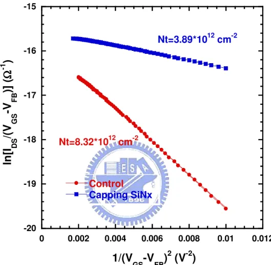
Fig. 2-4 shows the plot of ln[IDS/(VGS−Vfb)] versus 1/(VGS−Vfb) 2
at low drain voltage and high gate voltage for the control and the Capping Nitride samples. The
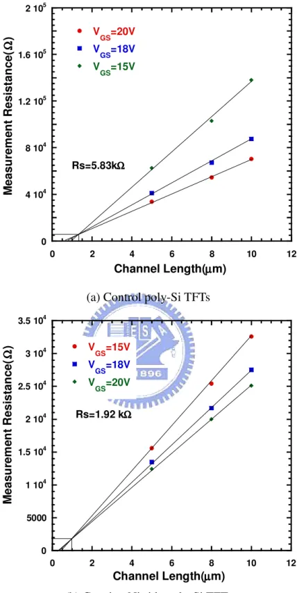
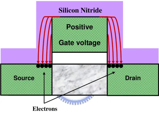
effective trap state density calculated from the slopes for the control and Capping Nitride samples were 8.32*1012cm-2 and 3.89*1012cm-2, respectively. The proposed poly-Si TFTs have less trap state density then the control samples, we deduced that proposed poly-Si TFTs have NH3 plasma treatment when deposited silicon nitride layer. Fig. 2-5 shows Source/drain series resistance extraction of (a) the Control and (b) the Capping Nitride poly-Si TFTs. We found that Capping Nitride poly-Si TFTs’ series resistance is small than the control poly-Si TFTs. They were found to be 5.83kΩ and 1.92kΩ for the control and Capping Nitride poly-Si TFTs, respectively. This result attributed nitride layer induced electron in source/drain region when device operated. So, source/drain series resistance are decreased. The schematic diagram of the mechanical of source/drain series resistance reduction is shown in Fig. 2-6.
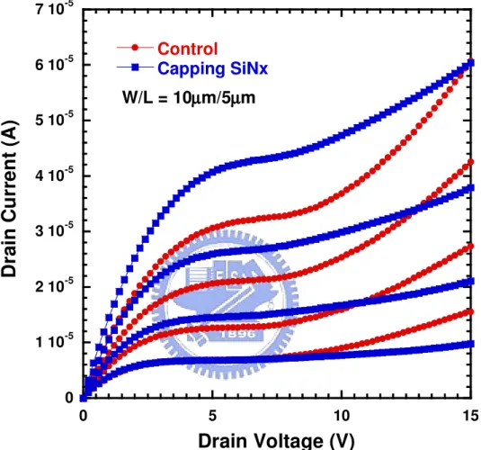
Fig.2-7 shows the output characteristics of the control and proposed poly-Si TFTs. It can be seen that the kink effect was suppressed in Capping Nitride poly-Si TFTs and saturation current greatly enhanced. This is attributed to the facts that nitride layer reduce horizontal electrical field [12] and further reduce impact ionization rate, the carrier that pile up in the channel is decreasing. So, kink effect was suppressed in Capping Nitride poly-Si TFTs. However, the enhancement of saturation current is due to high field effect mobility.
2.4.2
Reliability of poly-Si TFTs with capping silicon nitride layer
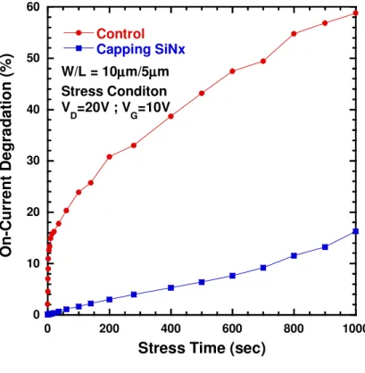
Furthermore, we discussed the reliability of proposed TFTs and convention TFTs. We apply DC stress to the device, the hot carrier stress test was performed at VD=20V, VG=10V, and source electrode grounded for 1000 sec to investigate the device reliability. Fig. 2-8 shows the variation of the on-state current (Ion) and threshold
voltage (Vth) over hot carrier stress time. The variations of Ion and Vth were defined as (Ion,stressed-Ion,initial)/Ion,initial*100% and (Vth,stressed-Vth,initial)/Vth,initial*100%, respectively, where Ion,stressed, Vth,stressed, Ion,initial, and Vth,initial represent the measured values before and after electrical stress.
Notably, the control shows relatively large variations in Ion, and Vth after 1000sec stress. These results imply that Capping Nitride poly-Si TFTs greatly reduced the device degradation under hot carrier stress, this is attributed to the fact that similarly high-k spacer structure can reduce horizontal electrical field [12] and then decrease the impact ionization rate. So, the Capping Nitride poly-Si TFTs have better reliability then the control samples.
2.5
Summary
We fabricated high performance TFTs with capping silicon nitride layer. The characteristic of proposed TFTs have great improvement, such as higher on-current, higher mobility, lower subthreshold swing, suppressing kink effect and GIDL effect and good reliability. The process of proposed TFTs is uncomplicated and no need of extra mask step. We believe that the proposed TFTs will be candidate in high performance TFTs application.
Reference:
[1] Y. Chen, J. Au, P. Kazlas, A. Ritenour,H. Gates, and J. Goodman, “Ultrathin, high-resolution, flexible electronic ink displays addressed by a-Si active-matrix TFT backplanes on stainless steel foil,” in IEDM Tech. Dig., 2002, pp. 389–392. [2] M. G. Kane, J. Campi, M. S. Hammond, F. P. Cuomo, B. Greening, C. D. Sheraw,
J. A. Nichols, D. J. Gundlach, J. R. Huang, C. C. Kuo, L. Jia, H. Klauk, and T. N. Jackson, “Analog and digital circuits using organic thin-film transistors on polyester substrates,” IEEE Electron Device Lett., vol. 21, pp. 534–536, Nov. 2000.
[3] J. Engel, J. Chen, C. Liu, B. R. Flachsbart, J. C. Selby, and M. A. Shannon, “Development of polyimide-based flexible tactile sensing skin,” in Proc. Mat. Res.
Soc. Symp., vol. 736, 2003, pp. D.4.5.1–D4.5.6.
[4] H. Gleskova, S. Wagner, W. Soboyejo, and Z. Suo, “Electrical response of amorphous silicon thin-film transistors under mechanical strain,” J. Appl. Phys., vol. 92, pp. 6224–6229, 2002.
[5] S. Maikap, C.-Y. Yu, S.-R. Jan, M. H. Lee, and C. W. Liu, “Mechanically Strained Strained-Si NMOSFETs,” IEEE Electron Device Lett., vol. 25, no. 1 pp. 40–42, 2004.
[6] Pai-hui Iris Hsu , M. Huang, H. Gleskova, Z. Xi, Z. Suo, S. Wagner, and James C. Sturm, “Effects of Mechanical Strain on TFTs on Spherical Domes” IEEE Trans.
Electron Devices, vol. 51, no. 3, pp. 371-377, 2004
[7] J. L. Hoyt, H. M. Nayfeh, S. Eguchi, I. Aberg, G. Xia, T. Drake, E. A. Fitzgerald, and D. A. Antoniadis, “Strained Si MOSFET technology,” in IEDM Tech. Dig., 2002, p. 23.
[8] K. Rim, S. Narasimha, M. Longstreet, A. Mocuta, and J. Cai, “Low field mobility characteristics of sub-100 nm unstrained and strained Si MOSFETs,” in IEDM
[9] C. H. Chen, T. L. Lee, T. H. Hou, C. L. Chen, C. C. Chen, J.W. Hsu, K. L. Cheng, Y. H. Chiu, H. J. Tao, Y. Jin, C. H. Diaz, S. C. Chen, and M. S. Liiang, “Stress memorization technique (SMT) by selectively strained-nitride capping for sub-65 nm high-performance strained-Si device application,” in Symp. VLSI Tech. Dig., 2004, pp. 56–57.
[10] S. Ito, H. Namba, K. Yamaguchi, T. Hirata, K. A. S. Koyama, S. Kuroki, N. Ikezawa, T. Saitoh, and T. Horiuchi, “Mechanical stress effect of etch-stop nitride and its impact on deep submicron transistor design,” in IEDM Tech. Dig., 2000, pp. 247–250.
[11] Tsung Yi Lu and Tien Sheng Chao, “Mobility Enhancement in Local Strain Channel nMOSFETs by Stacked a-Si/Poly-Si Gate and Capping Nitride,” IEEE
Electron Device Lett., vol. 26, no. 4 pp. 267–269, 2005.
[12] Zhibin Xiong, Haitao Liu, Chunxiang Zhu and Johnny K. O. Sin, “Characteristics of High-k Spacer Offset-Gated Polysilicon TFTs,” IEEE Trans.
(a) Thermal oxidation grown by furnace
(b) Amorphous Si (a-Si) deposited by LPCVD
(c) Recrystallization of a-Si film into poly-Si channel by SPC, active region defined
Si Wafer
Thermal Oxide
Poly-Si Channel
Si Wafer
Thermal Oxide
a-Si
Si Wafer
Thermal Oxide
(d) Deposition of TEOS gate oxide by LPCVD and poly-Si gate by LPCVD
(e) The gate electrode defined and self-align phosphorous ion implantation
Si Wafer
Thermal Oxide
Poly-Si Channel
Phosphorous self-aligned ion implantation
Si Wafer
Thermal Oxide
Poly-Si Channel
TEOS Gate Oxide
(f) Dopant activation by excimer laser annealing
(g) Deposition of silicon nitride layer and passivation oxide by PECVD
Si Wafer
Thermal Oxide
Poly-Si
n
+n
+n
+Si Wafer
Thermal Oxide
Poly-Si
n
+n
+n
+(h) Contact holes opened and metal pads formation
Fig 2-1 Schematic diagram of fabrication process for Capping Nitride poly-Si TFTs
Si-Wafer
Thermal Oxide
Poly-Si
n
+Table 2.1 Comparison of device characteristics of the Control and Capping Nitride poly-Si TFTs.
Poly-Si TFTs
Control
Capping Nitride
V
th(V)
0.67
0.16
S.S (V/dec.)
1.25
0.98
µ
Eff(cm
2/V.s)
23
32.5
I
on@ VG=20V
1.08*10
-41.60*10
-4I
off@ VG=-10V
1.61*10
-91.71*10
-10Rs (
Ω)
5.83*10
31.92*10
3N
t(cm
-2)
8.32*10
123.89*10
1210-12 10-10 10-8 10-6 10-4 -10 -5 0 5 10 15 20
Control
Capping SiNx
D
ra
in
C
ur
re
nt
(A
)
Gate Voltage (V)
W/L = 10µµµµm/10µµµµm
V
D= 5V
Fig. 2-2 Transfer characteristics of the Control and Capping Nitride poly-Si TFTs with VDS=5V
-5 0 5 10 15 20 25 30 35 -10 -5 0 5 10 15 20 Control Capping SiNx
Fi
eld
Ef
fe
ct
M
ob
ili
ty
, µµµµ
ef f(c
m
2/v
.s
ec
)
Gate Voltage, V
G(V)
W/L = 10µµµµm/10µµµµm Oxide thickness = 50nm VDS=0.1VFig. 2-3 Field-effect mobility of the Control and Capping Nitride poly-Si TFTs with VDS=0.1V
-20 -19 -18 -17 -16 -15 0 0.002 0.004 0.006 0.008 0.01 0.012
Control
Capping SiNx
ln
[I
DS/(V
G S-V
FB)]
(ΩΩΩΩ
-1)
1/(V
GS-V
FB)
2(V
-2)
Nt=8.32*10
12cm
-2Nt=3.89*10
12cm
-2Fig. 2-4 Trap state density extraction of the Control and the Capping Nitride poly-Si TFTs
0 4 104 8 104 1.2 105 1.6 105 2 105 0 2 4 6 8 10 12 VGS=20V VGS=18V VGS=15V M easu rem en t R esi st an ce( ΩΩΩΩ ) Channel Length(µµµµm) Rs=5.83kΩΩΩΩ
(a) Control poly-Si TFTs
0 5000 1 104 1.5 104 2 104 2.5 104 3 104 3.5 104 0 2 4 6 8 10 12 VGS=15V VGS=18V VGS=20V M easu rem en t R esi st an ce( ΩΩΩΩ ) Channel Length(µµµµm) Rs=1.92 kΩΩΩΩ
(b) Capping Nitride poly-Si TFTs
Fig. 2-5 Source/drain series resistance extraction of (a) the Control and (b) the Capping Nitride poly-Si TFTs
Fig. 2-6 Mechanism of reduction of source/drain series resistance
Positive
Gate voltage
Source
Drain
Electrons
Silicon Nitride
0 1 10-5 2 10-5 3 10-5 4 10-5 5 10-5 6 10-5 7 10-5 0 5 10 15
Control
Capping SiNx
D
ra
in
C
ur
re
nt
(A
)
Drain Voltage (V)
W/L = 10µµµµm/5µµµµm
0 10 20 30 40 50 60 0 200 400 600 800 1000 Control Capping SiNx O n-C ur re nt D eg ra da tio n (% )
Stress Time (sec)
W/L = 10µµµµm/5µµµµm Stress Conditon VD=20V ; VG=10V
(a) On-current degradation with stress time
0 1 2 3 4 5 6 0 200 400 600 800 1000 Control Capping SiNx Th re sh ol d V ol ta ge Sh ift (V )
Stress Time (sec)
W/L = 10µµµµm/5µµµµm Stress Conditon VD=20V ; VG=10V
(b) Threshold voltage degradation with stress time
Fig. 2-8 (a) on-current and (b) threshold voltage degradation as a function of stress time under hot-carrier stress
Chapter 3
Characteristic and Reliability of P-Channel Poly-Si
TFTs with Multi-Channel Structure
3.1
Introduction
P-channel poly-Si TFTs have been used for many applications, such as low-power SRAMs [1], High-Resolution Active Matrix [2] and EEPROM’s [3]. In circuit design, CMOS technique is a very important technique. Because it have many advantage such as low power consumption, fully restored logic and better reliability. We would like realized CMOS technique by using TFTs device. So P-Channel and N-Channel TFTs are needed for integrated CMOS circuit. We believed that Poly-Si TFTs technology is the most promising candidate for the ultimate goal of building fully integrated flat panel display system-on-glass. Moreover, the stability of p-channel polysilicon TFTs has not been investigated as much as n-channel polysilicon TFTs. So, we discussed characteristic and reliability of P-Channel poly-Si TFTs in this chapter.
It is well know that the characteristics of poly-Si TFTs are dominated by the large trap density in poly-Si film. When channel width scaled down, devices are reported to exhibit better performance such as lower threshold voltage and smaller trap density [4]-[6]. As a result, Poly-Si TFTs with narrow and multiple channels have been proposed to improve device performance [7][8]. Previous reports indicated that the existence regions near the poly-Si pattern edge where the grain boundary trap density is much smaller than elsewhere in the poly-Si film [4]. When channel width