國立交通大學
電子工程學系電子研究所
博 士 論 文
一種新穎自行開發之快速精準量子模擬器
用於三維度高應力下矽電洞能帶結構及反
置層遷移率之研究
A New In-House Fast Sophisticated Quantum Simulator for
Silicon Hole Band Structure and Inversion-Layer Mobility
under Three-Dimensional GPa-Level Stresses
研究生: 李建志
指導教授: 陳明哲 博士
一種新穎自行開發之快速精準量子模擬器
用於三維度高應力下矽電洞能帶結構及反
置層遷移率之研究
A New In-House Fast Sophisticated Quantum Simulator for
Silicon Hole Band Structure and Inversion-Layer Mobility
under Three-Dimensional GPa-Level Stresses
研 究 生: 李建志 Chien-Chih Lee
指導教授: 陳明哲 博士 Dr. Ming-Jer Chen
國立交通大學
電子工程學系 電子研究所
博士論文
A DissertationSubmitted to Department of Electronics Engineering & Institute of Electronics
College of Electrical and Computer Engineering National Chiao Tung University
in Partial Fulfillment of the Requirements for the Degree of Doctor of Philosophy
in
Electronics Engineering November 2012
Hsinchu, Taiwan, Republic of China
一種新穎自行開發之快速精準量子模擬器
用於三維度高應力下矽電洞能帶結構及反
置層遷移率之研究
研究生: 李建志 指導教授: 陳明哲 博士
國立交通大學
電子工程學系 電子研究所博士班
摘要
對於持續微縮的電子元件,除了將會面對額外的量子侷限效應(不論是電場 造成的量子侷限或是空間造成的量子侷限)之外,亦會面對複雜的機械應力(不 論是有意或是無意的任何方向應力)。這兩個現象皆會對價電子能帶結構造成關 鍵的影響,進而大大地改變電洞的電特性。換句話說,這將會在理論工作上造成 額外的複雜程度和沉重的計算負擔。但是因為電洞特性的計算,例如電洞遷移率, 完全根據價電子能帶結構來進行計算,所以並不意外,令人滿意的電性計算結果 需要精細和高品質的價電子能帶結構計算來達成。此論文聚焦在電子元件p型反 置層中的電洞特性,而我們自行開發的模擬器是根據六能帶k‧p 薛丁格·波松方 程自洽方法來達成。 此論文主要的目的是:研究在顯著的量子侷限效應和複雜的應力影響下矽的 反置層電洞特性。而根據此主題,論文的組織結構如下。首先,我們將介紹在p 型反置層中價電子能帶結構。接下來,聚焦於 p-NEP 的數值計算方法和物理模型,然而根據 p-NEP 的數值演算方法,電腦處理器計算時間會非常地漫長。因 此,我們提出一個新穎的演算加速器,能本質地提升六能帶k‧p 薛丁格·波松的 自洽模擬速度。此演算加速器是經由一個三角位能井為主的六能帶k‧p 模擬器, 一個電洞等效質量近似技巧,和一個與導帶電子版本相近的薛丁格·波松自洽計 算器所組成。加速器會輸出一個接近實際量子侷限靜電位能的初始解,且對不同 的溫度、不同基板參雜濃度、反置層電洞濃度和表面晶格方向皆可行。其他論文 發表的計算是支持我們(001)和(110)基板晶格方向的計算結果。全部的電腦處理 器計算時間被減少到接近8%沒有加速器的計算時間。加速器更普遍的應用也會 在此說明。 接著,根據三組互異並以塊材為導向的Luttinger 參數 γ1, γ2, 和 γ3,以塊材 為導向的Luttinger 參數在六能帶 k‧p 薛丁格·波松方程自洽方法的可行性被確認。 以塊材為導向的 Luttinger 參數計算,(110)基板方向p型場效電晶體之實際電洞
子能帶結構可以被良好地重現,並與最近 Takahashi 等人的 Shubnikov-de Haas (SdH)迴旋共振實驗比較。 更進一步,沿著三個晶格方向的單軸 GPa 等級應力造成的電洞遷移率變化 可以分為四個分別的貢獻來討論:一、聲子震盪限制,二、表面粗糙限制,三、 散射時間限制,四、傳導質量限制下的遷移率變化。在同一討論中,我們致力研 究應力相關的三個材料參數,也是所謂的Bir-Pikus 形變電位參數 a, b, 和 d。並 且,在數值上有著廣闊的分布。為了克服如此明顯的不一致性,我們詳盡地計算 電洞反置層遷移率,發現了沿著單軸<110>方向的壓縮應力對電洞遷移率增加而 言,a 影響微弱,b 影響適中,而 d 影響劇烈。以上的結論提供了指引透過實 驗決定主要參數d,次要參數 b,及一般使用的 a數值。另外,p-NEP 的使用者 介面(UI)和模擬程序會示範操作,模擬的子能帶結構、臨界電壓、電容和閘 極直接穿隧電流會被討論。最後,我們將總結研究結論。
關鍵字:量子侷限效應、機械應力、價電子能帶結構、六能帶k‧p 薛丁格·波松
A New In-House Fast Sophisticated Quantum Simulator for
Silicon Hole Band Structure and Inversion-Layer Mobility
under Three-Dimensional GPa-Level Stresses
Student: Chien-Chih Lee Advisor: Dr. Ming-Jer Chen
Department of Electronics Engineering and Institute of Electronics
National Chiao Tung University
Hsinchu, Taiwan
Abstract
The continuously scaled electronic devices encounter not only the extra quantum confinement (no matter from the field confinement or from the space confinement) but also the complicated mechanical stresses (no matter the intentional or unintentional stressors along the arbitrary directions). Both of these two phenomena cause the crucial impacts on the valence-band structure which can greatly alter the hole electrical properties. In other words, these lead to the extra complexities and the heavy computation burden in the theoretical work. Since the evaluation of the hole electrical properties such as hole mobility fully rely on the valence subband structures, with no surprise the precise and fine quality of valence subband structures are urgently required to achieve the satisfactory calculations. With the six-band k‧p
Schrödinger-Poisson self-consistent method this dissertation will focus on the hole electrical properties in p-type inversion layer of the electronic devices via the self-developed simulator, p-NEP (abbreviation of p-type Nano Electronics Physics).
properties in silicon inversion layer beneath on the significant quantum confinement and the complicated mechanical stresses. Based on this main topic, the organization of this dissertation is described below.
First, an introduction to the valence band structures in p-type inversion layer is described. Then, the dissertation is focused on the numerical techniques and physical models of p-NEP. However, according to the algorithm of p-NEP, the CPU time is extraordinarily long. To overcome the issue, we present a novel computational accelerator to intrinsically boost a self-consistent six-band k‧p Schrödinger-Poisson simulation. This accelerator comprises a triangular potential based six-band k‧p simulator, a hole effective mass approximation (EMA) technique, and an electron analogue version of the self-consistent Schrödinger and Poisson’s equations solver. The outcome of the accelerator furnishes the initial solution of the confining electrostatic potential and is likely to be close to the realistic one, valid for different temperatures, substrate doping concentrations, inversion hole densities, and surface orientations. The results on (001) and (110) substrates are supported by those published in the literature. The overall CPU time is reduced down to around 8% of that without the accelerator. The application of the proposed accelerator to more general situations is projected as well.
Secondly, according to three distinct sets of the bulk oriented Luttinger parameters γ1, γ2, and γ3, the validity of the bulk oriented Luttinger parameters in the six-band k‧p Schrödinger-Poisson self-consistent method is confirmed. With the the
bulk oriented Luttinger parameters, the realistic hole subband structures in (110) p-MOSFETs can be well reproduced in comparison with the recent Shubnikov-de Haas (SdH) oscillation experiment by Takahashi, et al.
three crystallographic directions are distinguished into four contributing componds: (i) phonon-limited, (ii) surface-roughness-limited, (iii) scattering-time-limited, and (iv) conductive-mass-limited mobility changes. It is also dedicated to three key strain-related material parameters, namely the Bir-Pikus deformation potentials a, b,
and d, which are widespread in magnitude. To improve such large discrepancies, we conduct sophisticated calculations on <110>/(001) and <110>/(110) hole inversion-layer mobility. We find that, to affect the calculated hole mobility enhancement, a is weak, b is moderate, and d is strong, particularly for the uniaxial
compressive stress along the <110> direction. This provides guidelines for an experimental determination of the primary factor, d, and the secondary factor, b, with the commonly used values for a. The user interface (UI) and simulation process of
p-NEP are further demonstrated. The resulting subbnad structures, threshold voltage,
capacitance, and gate direct tunneling current are all addressed. Finally, we summarize the conclusions of our works.
Keyword: quantum confinement, mechanical stress, valence-band structure, six-band
k‧p Schrödinger-Poisson self-consistent method, Luttinger parameters, Bir-Pikus
謝誌
在漫漫求學長路上,能有幸完成此博士論文,首先必須感謝我的內人,如怡, 以及父親,裕瑞、母親,雯彣、及弟弟,建穎。因為每當遭遇了看似過不了的難 關時,他們的精神支持總是給予最大的力量,讓我一躍而過。還有我的岳父,清 任及岳母,美惠,感謝他們信任及關心,並也感謝每一位親愛家人的由衷關心。 最重要的是要感謝我的指導教授,陳明哲老師,他對學術的真誠熱情激發了每位 學生的潛能,更重要的是對每位學生無私的關心。老師的一句話「歸零」,直到 現在都還深深影響著我,每當在研究或生活上遇到難解的問題時,都會先讓心態 歸零清空,然後再來解決問題,這給予我莫大的幫助。 非常感恩口試委員,胡振國教授、鄭舜仁教授、林鴻志教授、簡昭欣教授、 余宗興經理、以及吳忠政處長的百忙中抽空指導,每一位口試委員所提出的精闢 見解皆有助我釐清盲點和提升視野,獲益良多。 另外,要感謝師母侯錦珊女士、實驗室呂明霈、林大文學長總是在我沒有頭 緒時,提出了精闢的方向。感謝實驗室學弟妹寬豪、霖祥、宛勵的相助,及韋漢、 立鳴、宮強和每位學弟妹同仁的技術支援和戰友情誼。也要感謝在德國的友人: Thomas Seyller 教授、Peter Wehrfritz、Beate 和 Matthias 讓我在異地仍感受 到溫暖。最後,要把此論文獻給還待在老婆肚子中的兒子,親愛的外公外婆,以及在 上天眷顧著我們的爺爺和奶奶。因為,於戰亂而離鄉背井的大時代裡,沒有他們 在台灣這片土地上的艱辛開拓,就沒有我們現在的一絲一毫成就。
Table of Contents
Chinese Abstract i
English Abstract iii
Acknowledgement vi
Table of Contents vii
Table Captions x
Figure Captions xii
Chapter 1
1
Introduction to Valence-Band Structure in p-type Inversion Layer 1
1.1 Overview 1
1.2 Dissertation Organization 3
References 6
Chapter 2
11
Simulation Tool: p-NEP 11
2.1 Introduction 11
2.2 Numerical Techniques 11
2.2.1 Time-independent Schrödinger and Poisson’s Equations: Matrix
Techniques 11
2.2.2 Six-Band k‧p Schrödinger-Poisson Self-Consistent Method 15
2.3 Physical Models 18
2.3.1 Kubo-Greenwood Formula 18
2.3.2 Acoustic Phonon Scattering 19
2.3.4 Surface Roughness Scattering 20 2.3.5 WKB Based Hole Gate Direct Tunneling 21
2.3.6 Stress-to-Strain Tensor 23
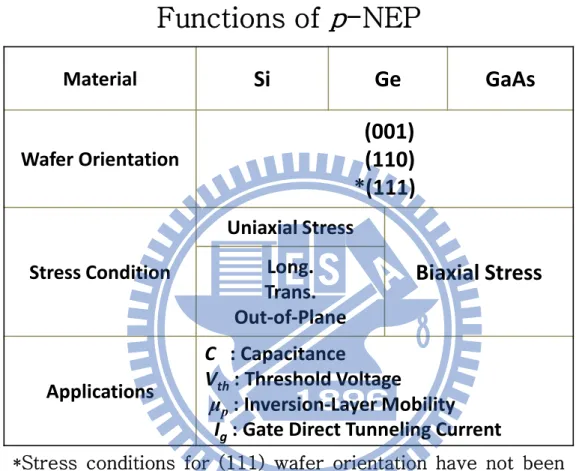
2.4 Functions of p-NEP 24
References 26
Chapter 3
35
Computational Booster in p-NEP 35
3.1 Introduction 35
3.2 Computational Booster 37
3.2.1 Triangular Potential Based Six-Band k‧p Method 37 3.2.2 Hole Effective Mass Approximation Technique 38
3.2.3 Core Accelerator 39
3.3 Results and Discussions 41
3.4 Projection 43
References 45
Chapter 4
62
Hole Band Structure and Inversion-Layer Mobility Calculation at 2
K 62
4.1 Introduction 62 4.2 γ1, γ2, and γ3 Examination 63 4.3 Conclusions 65 References 66Chapter 5
83
Three-Dimensional GPa-Level Stress Altered Hole Mobility in (001)
and (110) Silicon Inversion Layers
83
5.1 Introduction 83
5.2 Phonon and Surface-Roughness Limited Hole Mobility Changes 84
5.3 Scattering Time and Conductivity Mass Limited Hole Mobility
Changes 86
5.4 Effect of Strained k p Deformation Potentials on Hole Mobility‧ 88
5.4.1 Effect of Bir-Pikus Deformation Potentials 89 5.4.2 Guidelines and Experimental Determination 90
5.5 Conclusions 92
References 94
Chapter 6
130
Demonstration of p-NEP 130
6.1 User Interface (UI) and Simulation Process 130
6.2 Demonstration Results 132
6.2.1 Hole Subband Structure 132
6.2.2 Hole Inversion-Layer Mobility 132
6.2.3 Hole Gate Direct Tunneling and Capacitance 132
References 134
Chapter 7
157
Conclusions 157
Table Captions
Chapter 2
Table 2.1 The function list of p-NEP. The stress conditions in (111) wafer orientation have not been completed.
Table 2.2 The operational range list of p-NEP. Note that the operational range is not equal to the limitation range. The operational range in this table has been verified by the convergent error and reasonable outputs.
Chapter 4
Table 4.1 The list of the widely used bulk oriented Luttinger parameters mentioned in the Lawaetz's and Humphreys's published literatures[2], [3].
Chapter 5
Table 5.1 List of scattering parameters and Bir-Pikus potentials used in Section 5.2 and 5.3. Notice that the scattering parameters used in Section 5.2 and 5.3 are assumed to be independent of the Bir-Pikus potentials av, b, and d. 29 30 67 98
Table 5.2 List of the modified scattering parameters and Bir-Pikus potentials used in Section 5.4.
Table 5.3 Material parameters used in Section 5.4. γ1, γ1, and γ1 are
Luttinger parameters; av, b, and d are the Bir-Pikus potentials; d0
is the optical deformation potential; split-off is the split-off hole
energy; c11, c12, and c44 are the elastic coefficients; ρ and a0 are
the crystal density and lattice constant of silicon; and are the longitudinal and transverse sound velocity.
99 100
Figure Captions
Chapter 1
Fig. 1.1 Constant energy surfaces of heavy-hole, light-hole, and split-off-hole bulk valence bands in k-space at E-EΓ=25 meV.
Fig. 1.2 Comparison of existing algorithms [6]-[11], e.g. the constant effective mass as the conduction band counterpart, the six-band k‧p
method, and the pseudopotential method in combination with the Monte Carlo numerical technique, the iterative numerical technique, or the analytical triangular potential technique.
Fig. 1.3 Demonstration of the trade-off of the calculation efficiency and precision between above-mentioned algorithms.
Chapter 2
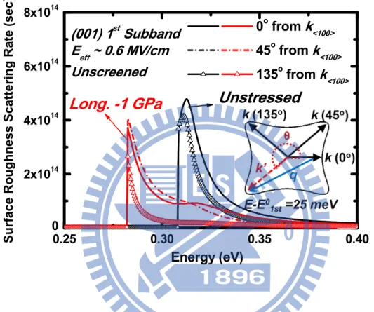
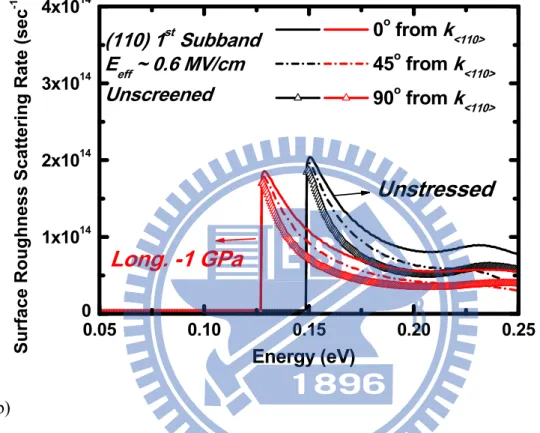
Fig. 2.1(a) Calculated intra-subband surface roughness scattering rate along the different k-direction of the first subband of (001) substrate with the longitudinal -1 GPa stress. The obvious angular dependence can be found in both cases.
Fig. 2.1(b) Calculated intra-subband surface roughness scattering rate along the different k-direction of the first subband of (110) substrate with the longitudinal -1 GPa stress. The obvious angular dependence can
8 9 10 31 32
be found in both cases.
Fig. 2.3 The Bir-Pikus deformation potential parameters are set as a= 2.46,
b= -2.1, and d= -4.85, showing the corresponding stress-strain
relationships under three-dimensional stresses on (001) p-MOSFET. Fig. 2.4 The Bir-Pikus deformation potential parameters are set as a= 2.46,
b= -2.1, and d= -4.85, showing the corresponding stress-strain
relationships under three-dimensional stresses on (110) p-MOSFET.
Chapter 3
Fig. 3.1 The flowchart of the simulation methodology in the inversion layer of pMOSFET. The methodology consists of two parts: the computational acceleration part in order to enhance the convergence speed and the self-consistent part in order to certify the tolerable error. The green blocks refer to the simulation methodology and the turquoise blocks refer to the outputs from the upper level simulator.
Fig. 3.2 The calculated hole quantization effective masses and DOS effective masses versus initial surface field in the simulation flowchart in Fig. 3.1.
Fig. 3.3 The calculated hole quantization effective masses and DOS effective masses versus initial surface field for different temperatures of 77, 153, and 300 K in the simulation flowchart in Fig. 3.1.
Fig. 3.4 Calculated (symbols) hole subband energy levels versus inversion carrier density on (001) surface. The solid lines come from De
33 34 47 48 49 50
Michielis, et al. [6] for comparison.
Fig. 3.5(a) Calculated (symbols) hole subband energy levels versus surface field on (001) substrate. The solid lines come from Low, et al. [8] for comparison.
Fig. 3.5(b) The corresponding surface potential versus surface field.
Fig. 3.6(a) Simulated DOS function for the first subband on (001) substrate in our work. The red and green solid lines are produced from the Cartesian and polar coordinate systems, respectively. The dotted line comes from [8] from comparison.
Fig. 3.6(b) Simulated DOS function for the total subbands on (110) substrate. The red and green solid lines are produced from the Cartesian and polar coordinate systems, respectively. The dotted line comes from [6].
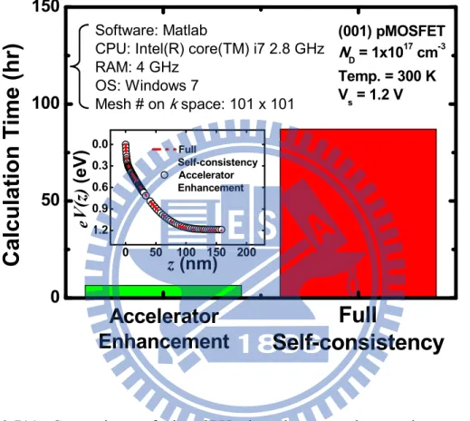
Fig. 3.7(a) Comparison of the CPU time between the accelerator enhanced methodology and the fully self-consistent methodology without the accelerator on (001) substrate. The inserted figure shows the corresponding electrostatic potential profiles.
Fig. 3.7(b) Comparison of the CPU time between the accelerator enhanced methodology and the fully self-consistent methodology without the accelerator on (110) substrate. The inserted figure shows the corresponding electrostatic potential profiles.
Fig. 3.8 Computational enhancement factor on (001) substrate versus the substrate doping concentration under the same inversion hole density of 11013 cm-2. Also shown are the corresponding CPU time with and without the accelerator.
51 52 53 54 55 56 57
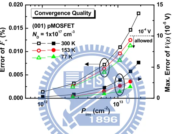
Fig. 3.9 The convergence quality on (001) substrate versus surface field at 77, 153, and 300 K. The convergence conditions in this work are: (i) below 1% error for the surface field and (ii) 10-4 V maximum error for the confining electrostatic potential profile.
Fig. 3.10 Comparison of the convergence quality having no Gummel iteration and that with the additional Gummel iteration, plotted as a function of the inversion hole density on (001) substrate at 300 K. Fig. 3.11 Comparison of the experimental gate capacitance versus gate
voltage curves [13] and those (only in weak inversion and strong inversion region) simulated with the convergence criterion of 10-4 V for the confining potential. From the HRTEM image [13], the nominal physical gate oxide thickness is 1.89 nm. However, in the simulation, three different physical gate oxide thicknesses were used to testify the validity of the chosen convergence criterion in this work.
Fig. 3.12 The calculated hole quantization effective masses and DOS effective masses versus initial surface field under unstressed and longitudinal -1 GPa stresses through the modified Eq. (3.4.1). The subbands are simply sorted by the most occupied hole type (heavy-hole-like, light-hole-like, and split-off-hole-like) in each subband.
Chapter 4
Fig. 4.1 Illustration of the experimental criteria [4] in the presence of
58 59 60 61 57 68
density-of-states functions under two bias conditions, VthL and VthH with 3 10 cm-3 substrate doping (N
sub) at 2 K. The abrupt Fermi distribution can ensure the proper switching.
Fig. 4.2 Low-temperature validity of p-NEP preliminarily confirmed by the simulated capacitance at 50 K by Schred [5] which adopts the constant mass self-consistent Schrödinger-Poisson method. Although the different methods of band structure calculations are made between Schred and our work, both self-consistent results still can offer a preliminary comparison.
Fig. 4.3 Low temperature validity of p-NEP preliminarily confirmed by the experimental hole effective mobility [6] at 77 K and 300 K.
Fig. 4.4 The situation with 10, 20, and 30 represented by the subband
energies and Fermi level versus gate volatge with 3 10 cm-3 substrate doping (Nsub) and 6 nm oxide thickness of SiO2 at 2 K. The simulation results are: VthL (Cal.)= -1.3 V, VthH (Cal.) = -2.3 V and
Ns(Cal.)(VthH) = 3.7 10 cm-2. The ccalculated VthH (Cal.) and
Ns(Cal.)(VthH) are closed to the experimental values [4].
Fig. 4.5 The impact of γ1 modulation on subband minimum of (110) p-MOSFETs. The triangular potential approximation is used to efficiently quantify this impact with 3 10 cm-3 substrate doping (Nsub) and fixed 0.25 MV/cm surface field (Fs).
Fig. 4.6 The impact of γ2 modulation on subband minimum of (110) p-MOSFETs. The triangular potential approximation is used to efficiently quantify this impact with 3 10 cm-3 substrate doping (Nsub) and fixed 0.25 MV/cm surface field (Fs).
69 70 71 72 73
Fig. 4.7 The impact of γ3 modulation on subband minimum of (110) p-MOSFETs. The triangular potential approximation is used to efficiently quantify this impact with 3 10 cm-3 substrate doping (Nsub) and fixed 0.25 MV/cm surface field (Fs).
Fig. 4.8 The impact of γ1 modulation on subband minimum of (001) p-MOSFETs. The triangular potential approximation is used to efficiently quantify this impact with 3 10 cm-3 substrate doping (Nsub) and fixed 0.25 MV/cm surface field (Fs).
Fig. 4.9 The impact of γ2 modulation on subband minimum of (001) p-MOSFETs. The triangular potential approximation is used to efficiently quantify this impact with 3 10 cm-3 substrate doping (Nsub) and fixed 0.25 MV/cm surface field (Fs).
Fig. 4.10 The impact of γ3 modulation on subband minimum of (001) p-MOSFETs. The triangular potential approximation is used to efficiently quantify this impact with 3 10 cm-3 substrate doping (Nsub) and fixed 0.25 MV/cm surface field (Fs).
Fig. 4.11 The calculated (001) total density-of-states functions using the three different sets in Table 4.1 for a triangular potential with Fs=1
MV/cm at 300 K.
Fig. 4.12 The calculated (110) total density-of-state functions using the three different sets in Table 4.1 for a triangular potential with Fs=1
MV/cm at 300 K.
Fig. 4.13 Comparison of calculated <110>/(110) hole mobility due to phonon and surface roughness scattering with the Luttinger parameters from Hensel [3] with the experimental <110>/(110) hole effective
74 75 76 77 78 79 80
mobility [8] at 50, 200, and 300 K.
Fig. 4.14 Comparison of calculated <110> and <001>/(110) hole mobility due to phonon and surface roughness scattering with the Luttinger parameters from Hesel [3] with the experimental hole effective mobility data [8] at 2K. Interface-trap- and ionized-impurity-limited hole mobility (empirical fitting) are involved in calculation using Matthiessen's rule. Note that the rms height of the amplitude of the surface roughness Δ is extracted to be 0.25 nm here which differs from the value in Fig. 4.13.
Fig. 4.15 Calculated density-of-states effective masses using the γ set from Hesel [3] with 3 10 cm-3 substrate doping (N
sub) at 2 K and 0 T.
The direct comparison with the measured cyclotron effective masses is shown.
Chapter 5
Fig. 5.1 Calculated 3-D uniaxial stress dependence of hole inversion-layer mobility change for different deformation potentials on (001) substrate. Comparison is done with other groups [8], [9]. The Bir-Pikus potentials av=2.1 eV, b=-1.6 eV, and d=-2.7 eV are cited
to the values in [6].
Fig. 5.2 Calculated 3-D uniaxial stress dependence of hole inversion-layer mobility change for different deformation potentials on (110) substrate. Comparison is done with other groups [8]. The Bir-Pikus potentials av=2.1 eV, b=-1.6 eV, and d=-2.7 eV are quoted to the
81 82 101 102
values in [6].
Fig. 5.3 The device structures for (001) and (110) p-MOSFETs. The channel direction and applied stress direction are clarified. Here, three-dimensional in-plane longitudinal, transverse and out-of-plane stress are involved in this dissertation.
Fig. 5.4 Mobility enhancement under longitudinal stress for different mobility components such as phonon- and surface-roughness-limited ones at Eeff = 1.1MV/cm in (001) p-MOSFET.
Fig. 5.5 Mobility enhancement under transverse stress for different mobility components such as phonon- and surface-roughness-limited ones at Eeff = 1.1MV/cm in (001) p-MOSFET.
Fig. 5.6 Mobility enhancement under out-of-plane stress for different mobility components such as phonon- and surface-roughness-limited ones at Eeff = 1.1MV/cm in (001) p-MOSFET.
Fig. 5.7 Mobility enhancement under longitudinal stress for different mobility components such as phonon- and surface-roughness-limited ones at Eeff = 1.2MV/cm in (110) p-MOSFET.
Fig. 5.8 Mobility enhancement under transverse stress for different mobility components such as phonon- and surface-roughness-limited ones at Eeff = 1.2MV/cm in (110) p-MOSFET.
Fig. 5.9 Mobility enhancement under out-of-plane stress for different mobility components such as phonon- and
103 104 105 106 107 108 109
surface-roughness-limited ones at Eeff = 1.2MV/cm in (110) p-MOSFET.
Fig. 5.10 The error of Matthiessen's rule for three-dimensional uniaxial stresses at Eeff = 1.1MV/cm in (001) p-MOSFET.
Fig. 5.11 The error of Matthiessen's rule for three-dimensional uniaxial stresses at Eeff = 1.2MV/cm in (110) p-MOSFET.
Fig. 5.12 Average scattering time and the extracted conductivity effective masses for three-dimensional uniaxial stresses in (001) p-MOSFET at Eeff = 1.1MV/cm.
Fig. 5.13 Average scattering time and the extracted conductivity effective masses for three-dimensional uniaxial stresses in (110) p-MOSFET at Eeff = 1.2MV/cm.
Fig. 5.14 The ratio of total mobility, average scattering time, reciprocal of conductivity effective mass and density-of-states effective mass under longitudinal stress in (001) p-MOSFET at Eeff = 1.1MV/cm.
Fig. 5.15 The ratio of total mobility, average scattering time, reciprocal of conductivity effective mass and density-of-states effective mass under transverse stress in (001) p-MOSFET at Eeff = 1.1MV/cm. Fig. 5.16 The ratio of total mobility, average scattering time, reciprocal of
conductivity effective mass and density-of-states effective mass under out-of-plane uniaxial stress in (001) p-MOSFET at Eeff = 1.1MV/cm.
Fig. 5.17 The ratio of total mobility, average scattering time, reciprocal of conductivity effective mass and density-of-states effective mass
110 111 112 113 114 115 116 117
under longitudinal uniaxial stress in (110) p-MOSFET at Eeff = 1.2MV/cm.
Fig. 5.18 The ratio of total mobility, average scattering time, reciprocal of conductivity effective mass and density-of-states effective mass under transverse uniaxial stress in (110) p-MOSFET at Eeff = 1.2MV/cm.
Fig. 5.19 The ratio of total mobility, average scattering time, reciprocal of conductivity effective mass and density-of-states effective mass under out-of-plane uniaxial stress in (110) p-MOSFET at Eeff = 1.2MV/cm.
Fig. 5.20 Calculated heavy-hole-like valence subband structures under the out-of-plane quantum confinement in the presence of longitudinal, transverse, out-of-plane stresses on (001) and (110) wafer orientations.
Fig. 5.21 Calculated <110> hole inversion-layer mobility change, from [6]-[9] and this work, plotted versus <110> uniaxial stress on (001) substrate.
Fig. 5.22(a) Calculated 3-D uniaxial stress dependence of hole inversion-layer mobility change for (001) substrate.
Fig. 5.22(b) Calculated 3-D uniaxial stress dependence of hole inversion-layer mobility change for (110) substrate.
Fig. 5.23 Calculated hole inversion-layer mobility enhancement values at two uniaxial compressive stresses for the reference deformation potentials and six different conditions (C1 to C6). The inset shows calculated DOS of 2 lowest subbands for C5 and C6.
118 119 120 121 122 123 124
Fig. 5.24 Flowchart showing the establishment of the guidelines with the mutual coupling between the Bir-Pikus deform potentials and Dac
taken into account.
Fig. 5.25 Comparison of experimental hole inversion-layer effective mobility (symbols) [21] and calculated hole universal mobility (lines) versus vertical effective electric field. The scattering parameters used are listed in Table 5.2 and apply to both (001) and (110) substrates.
Fig. 5.26 Experimental (symbols) <110> hole inversion-layer mobility enhancement [10],[11] versus <110> uniaxial compressive stress on (001) substrate. Calculation results in this work (lines) are shown for comparison. The inset depicts the case of biaxial stress with the experimental data from [23],[24].
Fig. 5.27 Comparisons of the calculated hole inversion-layer mobility change between the varying range of rms height of the surface roughness from 0.3 to 0.5 nm on (001) substrate with the interesting longitudinal compressive stress.
Fig. 5.28 Comparisons of the calculated hole inversion-layer mobility change between the exponential and Gaussian autocovariance function with and without the screening effect on (001) substrate with the interesting longitudinal compressive stress.
Chapter 6
Fig. 6.1 The basic structure of the simulator p-NEP.
125 126 127 128 129 135
Fig. 6.2 The UI for the main program of p-NEP in Fig. 6.1.
Fig. 6.3 The UI for the hole inversion-layer mobility program of p-NEP in Fig. 6.1.
Fig. 6.4 The UI for the hole gate direct tunneling program of p-NEP in Fig. 6.1.
Fig. 6.5 The UI for the threshold voltage and capacitance programs of
p-NEP in Fig. 6.1.
Fig. 6.6 The calculated subband levels based on the the six-band k‧p
triangular potential approximation versus the longitudinal stress in the (001) p-type silicon inversion layer.
Fig. 6.7 The calculated subband occupancy based on the the six-band k‧p
triangular potential approximation versus the longitudinal stress in the (001) p-type silicon inversion layer. The calculation conditions are the same as in Fig. 6.6.
Fig. 6.8 The calculated subband structures along k<110> based on the the
six-band k‧p triangular potential approximation versus the
longitudinal stress in the (001) p-type silicon inversion layer. The calculation conditions are the same as in Fig. 6.6.
Fig. 6.9 The fully-iterated (by the six-band k‧p Schrödinger-Poisson
self-consistent method) energy contours of the first subband in (001) silicon p-type inversion layer.
Fig. 6.10 The fully-iterated (by the six-band k‧p Schrödinger-Poisson
self-consistent method) energy contours of the first subband in (001) germanium p-type inversion layer.
Fig. 6.11 The fully-iterated (by the six-band k‧p Schrödinger-Poisson
136 137 138 139 140 142 142 143 144 145
self-consistent method) energy contours of the first subband in (001) gallium arsenide p-type inversion layer.
Fig. 6.12 The fully-iterated (by the six-band k‧p Schrödinger-Poisson
self-consistent method) group velocity along k<110> overall k-plane
of the first subband in (001) silicon p-type inversion layer.
Fig. 6.13 The fully-iterated (by the six-band k‧p Schrödinger-Poisson
self-consistent method) group velocity along k<110> overall k-plane
of the first subband in (110) silicon p-type inversion layer.
Fig. 6.14 The fully-iterated (by the six-band k‧p Schrödinger-Poisson
self-consistent method) acoustic phonon, optical phonon, and surface roughness scattering rate of the first subband in (001)
silicon p-type inversion layer.
Fig. 6.15 The fully-iterated (by the six-band k‧p Schrödinger-Poisson
self-consistent method) acoustic phonon, optical phonon, and surface roughness scattering rate of the first subband in (110)
silicon p-type inversion layer.
Fig. 6.16 The unstressed (001) and (110) hole inversion-layer mobility with and without screening effect with Nsub=1e17 cm-3 at Temp. =300
K.
Fig. 6.17 The calculated unstressed hole gate direct tunneling current density are found in the satisfactory agreements with the experimental data of the different oxide thicknesses [1].
Fig. 6.18 The unstressed capacitance versus gate voltage are compared with the experimental data from [2] where the stressor originated from the selective fully silicided (FUSI) gate.
146 147 148 149 150 151 152
Fig. 6.19 The stressed capacitance versus gate voltage are compared with the experimental data from [2] where the stressor originated from the selective fully silicided (FUSI) gate.
Fig. 6.20 The calculated hole gate direct tunneling current density and capacitance are drawn simultaneously with the varying poly-gate doping concentrations. The other parameters came from the table (poly-gate) in Fig. 6.19.
Fig. 6.21 The calculated hole gate direct tunneling current density and capacitance are drawn simultaneously with the varying stress conditions. The other parameters came from the table (poly-gate) in Fig. 6.19.
Fig. 6.22 The calculated hole gate direct tunneling current density and capacitance are drawn simultaneously with the varying metal-gate work functions. The other parameters came from the table (FUSI-gate) in Fig. 6.19. 153 154 155 156
Chapter 1
Introduction to Valence-Band Structure in
p-type Inversion Layer
1.1 Overview
As widely recognized, the method of so-called "effective mass theory" can describe the carriers moving in the perturbed periodic crystal field by introducing a mass tensor into Schrödinger equation. Through the cyclotron resonance experiments [1],[2],[3], the mass tensors of conduction band and valence band can be determined with some accuracy. However, different conduction and valence bands in diamond and zinc blende structure semiconductors such as silicon are found: (i) the top valence band locates at theΓ point of the first Brillouin zone, in contrast to the conduction band minimum near the first Brillouin zone edge along <100> directions, and (ii) within the perturbed energy range around Γ point, the conduction band structures have the more perfectly parabolic property than the obviously anisotropic and non-parabolic properties existing in the valence band structures as shown in Fig. 1.1 for heavy-, light-, and split-off-hole bands. Furthermore, the extra degeneracy at Γ point and the spin-orbit coupling, or even the applied mechanical strain all bring the
additional complexities in the valence band structures. In order to deal with the above complexities in the realistic valence band structures, Luttinger and Kohn [4] and Bir and Pikus [5] separately proposed the experiment associated Luttinger six-band k‧p
Hamiltonian and Bir-Pikus deformation potentials which importantly push forward the theoretical study on the strained valence band structures of diamond and zinc blende structure semiconductors.
Nowadays, the highly scaled electronic devices encounter not only the extra quantum confinement (no matter from the field confinement or from the space confinement) but also the complicated mechanical stresses (no matter the intentional or unintentional stressors from arbitrary directions). Both of these two phenomena cause the crucial impacts on the valence band structures which greatly alter the hole electrical properties. In other words, these lead to the extra complexity and the heavy computation burden in the theoretical work. To conclude the existing calculation methods to deal with the subband structure (due to the extra quantum confinement) in
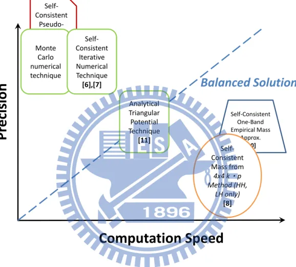
p-type inversion layer, Fig. 1.2 addresses several algorithms [6]-[11], e.g. the constant
effective mass as the conduction band counterpart, the six-band k‧p method, and the
pseudopotential method in combination with the Monte Carlo numerical technique [12], the iterative numerical technique [13], even or the analytical triangular potential technique. Then, we systematically explain the trade-off between these algorithms with the calculation efficiency and precision in Fig. 1.3. Since the evaluation of the hole electrical property such as hole mobility fully relies on the valence subband structures, with no surprise the precise and fine quality of valence subband structures are urgently required to achieve the satisfactory calculations. With the six-band k‧p
Schrödinger-Poisson self-consistent method as originally demonstrated by Bangert, von Klitzing and Landwehr [6] and by Ohkawa and Uemura [7], this dissertation will
focus on the hole electrical properties in p-type inversion layer of the electronic devices via the self-developed simulator, p-NEP.
1.2 Dissertation Organization
The main purpose of the dissertation is to investigate the hole electrical properties of the silicon inversion layer beneath in the presences of both the significant quantum confinement and the complicated mechanical stresses. Based on this main topic, the organization of this dissertation is described below.
First, an introduction to the valence band structures in p-type inversion layer is described in Chapter 1. Then, Chapter 2 of the dissertation is focused on the numerical techniques and physical models of p-NEP. About the numerical technique, the six-band k‧p Schrödinger-Poisson self-consistent method is used to obtain the
precise valence subband structures, inversion carrier distribution, and self-consistent potential profile. Concerning the physical models, (i) the phonon scattering rate, surface roughness scattering rate, and Kubo-Greenwood formula are used to achieve the elaborate transport calculation; (ii) the WKB approximation method is used to evaluate hole gate direct tunneling; and (iii) because of the highlighted three dimensional mechanical stresses in the dissertation, the stress-to-strain tensor is included as well. In general, p-NEP is a flexible simulator containing the functions of above calculations with the alternative materials (silicon, germanium, and gallium arsenide), the alternative wafer orientations ((001), (110), and (111)), the alternative
temperature conditions (2K to 400K), the alternative stress conditions (GPa-level uniaxial and biaxial stresses), and the alternative substrate doping concentrations (1x10¹⁵ to 6x1018 cm-3).
extremely heavy to remain the tolerable computation error. Thus, Chapter 3 presents a novel computational accelerator to intrinsically boost the self-consistent six-band
k‧p Schrödinger-Poisson simulation. This accelerator comprises a triangular
potential based six-band k‧p simulator, a hole effective mass approximation (EMA) technique, and an electron analogue version of the self-consistent Schrödinger and Poisson’s equations solver. The outcome of the accelerator furnishes the initial solution of the confining electrostatic potential and is likely to be close to the realistic one, valid for different temperatures, substrate doping concentrations, inversion hole densities, and surface orientations. The results on (001) and (110) substrates are supported by those published in the literature. The overall CPU time is reduced down to around 8% of that without the accelerator. The application of the proposed accelerator to more general situations is projected as well.
Secondly, according to three distinct sets of the bulk oriented Luttinger parameters γ1, γ2, and γ3, the validity of the bulk oriented Luttinger parameters in the six-band k‧p Schrödinger-Poisson self-consistent method is confirmed in Chapter 4.
With the bulk oriented Luttinger parameters, the realistic hole subband structures in (110) p-MOSFETs can be well reproduced in comparison with the recent Shubnikov-de Haas (SdH) oscillation experiment by Takahashi, et al.
Thirdly, the hole mobility change for GPa-level uniaxial stresses along each of three crystallographic directions are distinguished into four contributions: (i) the phonon-limited, (ii) the surface-roughness-limited, (iii) the scattering-time-limited, and (iv) the conductivity-effective-mass-limited mobility changes in Chapter 5. In the same chapter, it is also dedicated to three key strain-related material parameters, namely the Bir-Pikus deformation potentials a, b, and d, which are widespread in
calculations on <110>/(001) and <110>/(110) hole inversion-layer mobility. We find that, to affect the calculated hole mobility enhancement, a is weak, b is moderate,
and d is strong, particularly for the uniaxial compressive stress along the <110> direction. This provides guidelines for an experimental determination of the primary factor, d, and the secondary factor, b, with the commonly used values for a. In
Chapter 6, the user interface (UI) and simulation process of p-NEP are demonstrated. The resulting subbnad structures, threshold voltage, capacitance, and gate direct tunneling current are discussed. Finally, in Chapter 7 we summarize the conclusions of our works.
References
[1] G. Dresselhaus, A. F. Kip, and C. Kittel, “Observation of cyclotron resonance in germanium crystals,” Phys. Rev., vol. 92, no. 3, p. 827, Nov. 1953
[2] B. Lax, H. J. Zeiger, R. N. Dexter, and E. S. Rosenblum, “Directional properties of the cyclotron resonance in germanium,” Phys. Rev., vol. 93, no. 6, pp. 1418-1420, Mar. 1954.
[3] R. N. Dexer, H. J. Zeiger, and B. Lax, “Anisotropy of cyclotron resonance of holes in germanium,” Phys. Rev., vol. 95, no. 2, pp. 557-558, Jul. 1954.
[4] J. M. Luttinger and W. Kohn, “Motion of electrons and holes in perturbed periodic fields,” Phys. Rev., vol. 97, pp. 869-883, Feb. 1955.
[5] G. L. Bir and G. E. Pikus, “Theory of the deformation potential for semiconductors with a complex band structure,” Sov. Phys. Solid State, vol. 2, pp.2287-2300, Sept. 1960.
[6] E. Bangert, K. von Klitzing, and G. Landwehr, “Self-consistent calculations of electric subbands in p-type silicon inversion layers,” in Proceedings of the
Twelfth International Conference on the Physics of Semiconductors, Stuttgart,
edited by M. H. Pilkuhn (Teubner, Stuttgart, 1974), pp. 714-718.
[7] F. J. Ohkawa and Y. Uemura, “Hartree approximation for the electronic structure of a p-channel inversion layer of silicon M. O. S.,” Prog. Theor. Phys., no. 57, pp. 164-175, 1975.
[8] B. K. Ridley, Quantum Processes in Semiconductors, 3rd. ed. Oxford, U.K.: Clarendon , 1993, ch. 1.
[9] H. Nakatsuji, Y. Kamakura, and K. Tangiguchi, “A study of subband structure and transport of two-dimensional holes in strained-Si p-MOSFETs using full-band modeling,” in IEDM Tech. Dig., 2002, pp. 727-730.
[10] T. Low, Y. T. Hou, and M. F. Li, “Improved one-band self-consistent effective mass methods for hole quantization in p-MOSFET,” IEEE Trans. Electron
Devices, vol. 50, no. 5, pp. 1284-1289, May 2003.
[11] M. V. Fischetti, Z. Ren, P. M. Solomon, M. Yang, and K. Rim, “Six-band k‧p calculation of the hole mobility in silicon inversion layers: Dependence on surface orientation, strain, and silicon thickness,” J. Appl. Phys., vol. 94, no. 2, pp. 1079-1095, Jul. 2003.
[12] C. Jacoboni and P. Lugli, The Monte Carlo Method for Semiconductor Device Simulation, Springer-Verlag/Wien-New York, 1989.
[13] S. E. Laux and F. Stern, “Electron states in narrow gate-induced channels in Si,”
Fig. 1.1 Constant energy surfaces of heavy-hole, light-hole, and split-off-hole bulk valence bands in k-space at E-EΓ=25 meV.
-0.06 -0.04 -0.02 0 0.02 0.04 0.06 -0.05 0 0.05 -0.06 -0.04 -0.02 0 0.02 0.04 0.06 E-E = -25 meV -0.06 -0.04 -0.02 0 0.02 0.04 0.06 -0.05 0 0.05 -0.06 -0.04 -0.02 0 0.02 0.04 0.06 E-E = -25 meV -0.1 -0.05 0 0.05 0.1 0.15 -0.1 0 0.1 -0.1 -0.05 0 0.05 0.1 0.15 E-E = -25 meV Heavy‐Hole Band Light‐Hole Band Split‐off‐Hole Band kx(1/Å) kz (1 /Å ) kx(1/Å) kx(1/Å) kx(1/Å) kx (1 /Å ) kx(1/Å) kx(1/Å)
Fig. 1.2 Comparison of existing algorithms [6]-[11], e.g. the constant effective mass as the conduction band counterpart, the six-band k‧p method, and the pseudopotential
method in combination with the Monte Carlo numerical technique, the iterative numerical technique, or the analytical triangular potential technique.
Simulation in p‐type inversion layer Self‐Consistent Constant Mass from 4x4 k‧p Method (HH, LH only) [8] Six‐band k‧p Method (kzis replaced by the operator id/dz ) Analytical Triangular Potential Technique [11] Self‐ Consistent Iterative Numerical Technique [6],[7] Monte Carlo numerical technique Self‐ Consistent Pseudo‐ Potential Method [9] Self‐Consistent One‐Band Empirical Mass Approx. [10]
Fig. 1.3 Demonstration of the trade-off of the calculation efficiency and precision between above-mentioned algorithms.
Pr
ecision
Computation Speed
Balanced Solution
Self‐Consistent One‐Band Empirical Mass Approx. [10] Self‐ Consistent Mass from 4x4 k‧p Method (HH, LH only) [8] Analytical Triangular Potential Technique [11] Self‐ Consistent Pseudo‐ Potential Method [9] Monte Carlo numerical technique Self‐ Consistent Iterative Numerical Technique [6],[7]Chapter 2
Simulation Tool: p-NEP
2.1 Introduction
Herein, we will introduce our self-consistent solver, named as p-NEP, of coupled Poisson and Schrödinger’s equations in a six-band k‧p valence-band structure. It can apply to different surface orientations such as (001), (110), (111), and (11x) in general. And the strain Hamiltonian has already been incorporated into the solver. In Section 2.2, the detailed numerical techniques of p-NEP will be explained. Next, the physical models in order to calculate hole inversion mobility and gate direct tunneling current beneath under different stress conditions will be displayed in Section 2.3. Finally, the functions and operational range of p-NEP will be discussed and listed in a table.
2.2 Numerical Techniques
2.2.1
Time-independent Schrödinger and Poisson’s Equations:
Matrix Techniques
It is well-recognized that the time-independent Schrödinger equation in the quantum mechanics can be expressed in terms of a matrix equation:
2 2
2m V E
. (2.2.1.1) This approach is widely adopted in the band-structure simulation when it is focused on bound or quasi-bound states in a spatially varying potential V inside the highly scaled semiconductor devices. Let us assume that the wave-function is confined in a small region of W. We divide this region into intervals of the equal-distance
/
x W
. The ithmesh point is indexed as xi. In general, the wave-function we
are looking for can be expanded by an orthogonal basis set
nn n
n a
, (2.2.1.2) where the n is the normalized wave-function at the mesh point xn and the existingprobability of n is exactly zero outside the interval n. According to Eq. (2.2.1.1), the Schrödinger equation in the confined direction can be written numerically as
2 2 ( ) 2 ( ) ( ) [ ] ( ) ( ) ( ) 2 x x x x x V x x E x m x . (2.2.1.3)
Substituting Eq. (2.2.1.2) into Eq. (2.2.1.3), we get a set of equations (we are assuming a0 a10, i.e., the wave-function is localized in the space W). After taking the outer product of 1, , , 2 3 ... ,the matrix form of the one dimensional Schrödinger equation is presented by
1 2 3 (x ) 1 1 (x ) 2 2 (x ) (x ) 1 0 0 0 0 0 0 0 0 n A B a B A B a B A B a B A (2.2.1.4) with
i 2 ( )x ( )2 ( )i A V x E m x , (2.2.1.5) . (2.2.1.6) Obviously, Eq. (2.2.1.4) turns the complex differential Schrödinger equation into a common eigen-value problem and we will get the eigen-values corresponding to the eigen-function. The smallest eigen-value refers to the ground state while the others refer to the excited states.
For solving the Poisson equation with the matrix technique, there is a well-known numerical analysis of the Newton-Raphson method (or Newton-Fourier method) for finding successively better approximations to the zeros (or roots) of a real-value function. Newton’s method can converge remarkably quickly; especially if the iteration begins “sufficiently near” the desired root. First, we start with an initial value, for example v0, and look for the corresponding function of R. And then, the function is approximated by its sloped line, and one computes the V-intercept of this tangent line (which is easily done with elementary algebra). This V-intercept will typically be a better approximation to the function’s root than the original guess, and the method can be iterated. This iteration process can be expressed as
1 n n V V (2.2.1.7) V = ( ) R V R V (2.2.1.8)
Now, we write the 1D Poisson’s equation for N N matrix case as below:
2 2 V z (2.2.1.9)
2 2 1 1 2 2 2 2 2 2 2 2 1 1 2 2 2 1 0 0 1 2 1 0 1 2 1 0 0 1 2 0 0 N N N N N N z z V V z z z z z z V z z (2.2.1.10)
and let AV , where A is second-order differential matrix,
is carrier charge density: 2 2 2 2 2 2 2 2 2 2 2 1 0 0 1 2 1 0 1 2 1 0 0 1 2 0 0 N N z z z z z A z z z z z (2.2.1.11) 1 2 1 N N V V V V (2.2.1.12) 1 2 1 N N . (2.2.1.13)Finally, we apply Newton-Raphson method to solve Poisson and Schrődinger equations self-consistently. Therefore, we can hence express the Poisson equation as follows:
AV (2.2.1.14) R
and differentiate the Eq. (2.2.1.13) by V , we can obtain the following:
R A NR V V (2.2.1.15) and Eq. (2.2.1.8) can be rewritten as
R R V R NR V (2.2.1.16)
2.2.2
Six-Band k
‧
p Schrödinger-Poisson Self-Consistent Method
By following the theoretical work by Bangert, von Klitzing and Landwehr [1] and by Ohkawa and Uemura [2], a six-band silicon k‧p method, along with thesolving of Schrödinger and Poisson's equations in a self-consistent potential well beneath the gate oxide of bulk p-MOSFET, will be employed here. In this simulation framework, we solve the wave equation iteratively:
, , ∙ , , ∙ , , (2.2.2.1)
Here, e is the free electron charge, the confining electrostatic potential V(z) refers to
the solution of Poisson equation from the initial or previous iterative loop; and the
k‧p Hamiltonian Hkp is the Luttinger-Kohn Hamiltonian HLK [3] plus the strain
Hamiltonian Hstrain [4]. Those expressions are given in [5]. Therefore, the 6 6
1 0 2 2 3 0 2 2 3 0 2 2 1 0 2 2 1 3 2 2 0 2 2 3 1 2 2 0 2 2 kp LK strain P Q L M L M L P Q M Q L M P Q L L Q H H H M L P Q M L L Q L M P M L Q L P , (2.2.2.2) where k k k k P P P Q Q Q L L L M M M , (2.2.2.3)
2 2 2 2 1 0 2 2 2 2 2 0 2 3 0 2 2 2 2 3 0 2 2 2 3 3 2 2 k x y z k x y z k x y z k x y x y P k k k m Q k k k m L k ik k m M k k i k k m ;
2 2 3 2 v xx yy zz xx yy zz xz yz xx yy xy P a b Q L d i M b id . (2.2.2.4)the Pk, Qk, Lk, and Mk are the k p terms and the Pε, Qε, Lε and Mε are the strain
terms and is the split-off energy. The Luttinger parameters are γ1, γ2, and γ3, and the Bir-Pikus deformation potentials are a, b, and d.
,
d i
dz
and the quantization z-direction length (20 nm in this work) in the simulation is divided into a mesh of N points (z N =101 in this work). Contrary to the z
quantization region, the z-direction length of the bulk region is equal to maximum depletion width plus 400 nm additionally. Thus, focused on the quantization region, Eq. (2.2.2.1) becomes the 6Nz6Nz eigenvalue problem. Precisely speaking, this
6Nz6Nz eigenvalue matrix can be expressed as the tridiagonal block form
1 1 0 , , 1 0 , , 0 1 1 1 , , 0 0 ( , ) 0 0 0 0 x y x y x y x y x y x y l l k k k k l l l k k x y k k l l l l k k k k D D D E k k D D D D D D , (2.2.2.5)
where each k kx, y is a six-component column vector. D, D and D0 are 6 6
block-diagonal difference operators expressed as below
2 0 1 2 = + + kp z z H H H k H k , 1 2 2 2 ( ) H H D i z z , 0 2 0 2 2 ( ) H D H z , (2.2.2.6) 1 2 2 2 ( ) H H D i z z .
The solving of Eq. (2.2.2.5) yields the same number of the eigenvalue matrices,
E(kx,ky), as well as the wavefunction kx,ky(z). With the known equilibrium Fermi level Ef, the distribution of the total hole density per area Pinv(z) can be obtained as follows
∑ ∙ 1 exp , , (2.2.2.7)
where i is the subband index and is the wavefunction at the subband minimum. Then, to substitute Eq. (2.2.2.7) into the Poisson equation,
, (2.2.2.8) where and are the density of depleted ionized donors and free electrons in the depletion layer, the new surface potential V(z) can be obtained by the
Newton-Raphson method, followed by the next iterative loop via Eq. (2.2.2.1).
2.3 Physical Models
2.3.1
Kubo-Greenwood Formula
The outcomes of the solver p-NEP contain the hole subband energy level, the
Fermi level, the wave function, the DOS function, and the strained E-k structure. Then,
the hole inversion-layer mobility can be calculated using the Kubo-Greenwood formula [6]-[8]:
∑ 1
(2.3.1.1)
where e is the free electron charge, is the total hole density per unit area which sums along the z-direction, is the group velocity of subband μ along x direction, and f0 is the Fermi-Dirac distribution function in equilibrium. Under
the momentum relaxation time approximation, the total scattering time of subband μin (1) can relate to acoustic phonon scattering, optical phonon scattering, and surface roughness scattering through the expression:
. In this dissertation, eighteen lowest subbands were used in the mobility calculation.
2.3.2
Acoustic Phonon Scattering
We followed the isotropic treatment by Fischetti et al. [9] concerning acoustic
phonon scattering, but did not take into account the inelastic and dielectric screening effects of acoustic phonons in this work. The critical parameter, namely, the acoustic deformation potential Dac, is strongly connected to Bir-Pikus deformation potentials
[4],[10],[11]. According to Lawaetz [11], Dac can be formulated as
⁄ ;
;
, (2.3.2.1) where and are the average longitudinal and transverse elastic coefficients, respectively. , , and are the elastic coefficient elements whose values are listed in Table II. The elastic acoustic phonon scattering rate model used in this work is
∑ , (2.3.2.2)
where is equal to ⋅ ∗ , the wavefunction overlap
integral between the initial subband μ and the final subband ν. and denote the crystal density and the longitudinal sound velocity, respectively. Both intra- and inter-subband acoustic phonon scattering were considered in this work.
2.3.3
Optical Phonon Scattering
Optical phonon scattering involves the absorption and emission of optical phonons with the exchange of energy (61.2 meV in this dissertation). According to Wiley [12] and Costato and Reggiani [13], the optical deformation potential Dop can
have the following formalism:
, (2.3.3.1) where a0 is the lattice constant, d0 is the deformation potential of optical phonons, and
̅ is the average sound velocity consisting of the longitudinal and transverse sound velocity, and , respectively, with the formulation of ̅ 2 /3. Then, the isotropic absorbing and emitting optical phonon scattering rate can be written as
∑ ∓
∓ , (2.3.3.2) : optical phonon frequency,
: Bose occupation factor of optical phonons
Eq. (2.3.3.2) features both intra- and inter-subband optical phonon scattering but with no screening effect in this work.
2.3.4
Surface Roughness Scattering
To deal with surface roughness scattering, we first followed Pham, et al. [14] and
De Michielis, et al., [15] to take only the intra-subband scattering. Then, the screening
effect in the dielectric function as formulated by Yamakawa et al.[16] and Gámiz, et al. [17] was incorporated into the surface roughness scattering rate expression in the
context of the exponential autocovariance function:
∑
,
′ ′, (2.3.4.1)
∶ rms height of the amplitude of the surface roughness, ∶ correlation length of the surface roughness,
∶ angle between ′ and ,
∶ adjustable factor (= 1/2 in this work),
, ∶ , ∗ ⋅ ⋅ ⋅ ∗ ⋅ ⋅ ∗ ⋅ ,
: energy minimum of subband ν
: static wave-vector-dependent dielectric function,
1 ′ ′;
∑ ′ | | | | | ′|.
Importantly, Eq. (2.3.4.1) has the ability to adequately handle the angular dependence of surface roughness scattering, as shown in Fig. 2.1 in terms of the calculated unscreened scattering rate versus hole energy for both (001) and (110) substrates. It can also be seen from the figure that the scattering angular is more pronounced for GPa-level stress, especially on the (001) substrate.
2.3.5
WKB Based Hole Gate Direct Tunneling
According to the literatures [18]-[20],the isotropic hole direct tunneling current density contributed by the μth subband with WKB approximation can be written as
∙ ∙ ∙ , (2.3.5.1) ∑ , (2.3.5.2) where e denotes the elemental charge, is impact frequency of hole' wave packet on interface, is the inversion hole density of subband μ per energy per area,
is the transmission probability through insulator of WKB part, is the transmission probability through insulator of reflection part. There are eighteen subbands taken into account in our calculation. The impact frequency is described as
eF 2⁄ 2 , (2.3.5.3) Worth noting that the constant quantized effect mass in Eq. (2.3.5.3) approximately obtained by the triangular potential method will be discussed in Chapter 3. For the inversion hole density, we calculate it through
. (2.3.5.4) Two terms to be considered in the transmission probability through oxidelayer, the first one is WKB part, which can be modeled as
exp 2 exp / / | | , (2.3.5.5) | | , ,
where is the barrier height of the tunneling hole with total energy E at cathode
side or gate/oxideinterface, and is that at anode side or oxide/n-well interface with is the barrier height of oxide/Si interface. is an important parameter featuring the quantum transport in oxide. The WKB approximation is only valid when the wavefunction phase change is much smaller than the amplitude change, In other words, the barrier potential of oxide must be very sharp and high enough to ensure the validity of WKB method. Another transmission probability is , which is given as , , , | | , | | , (2.3.5.6) where , and , | | are the group velocities of the holes incident and leaving oxide. The semi-classical forms can be simply depicted as

![Fig. 6.19 The stressed capacitance versus gate voltage are compared with the experimental data from [2] where the stressor originated from the selective fully silicided (FUSI) gate](https://thumb-ap.123doks.com/thumbv2/9libinfo/8029422.161331/28.892.129.757.433.811/stressed-capacitance-compared-experimental-stressor-originated-selective-silicided.webp)