Characterization and field-emission properties of carbon nanotube arrays in
nanoporous alumina template and on blank Si substrate
Ching-Jung Yang, Chih Chen, and Jia-Min Shieh
Citation: Journal of Applied Physics 100, 104302 (2006); doi: 10.1063/1.2375012
View online: http://dx.doi.org/10.1063/1.2375012
View Table of Contents: http://scitation.aip.org/content/aip/journal/jap/100/10?ver=pdfcov Published by the AIP Publishing
Articles you may be interested in
Field emission of large-area and graphitized carbon nanotube array on anodic aluminum oxide template J. Appl. Phys. 93, 5602 (2003); 10.1063/1.1564882
Field emission property of highly ordered monodispersed carbon nanotube arrays Appl. Phys. Lett. 78, 3127 (2001); 10.1063/1.1372205
Template-based carbon nanotubes and their application to a field emitter Appl. Phys. Lett. 78, 2052 (2001); 10.1063/1.1359483
In situ-grown carbon nanotube array with excellent field emission characteristics Appl. Phys. Lett. 76, 3813 (2000); 10.1063/1.126790
Controlling growth and field emission property of aligned carbon nanotubes on porous silicon substrates Appl. Phys. Lett. 75, 481 (1999); 10.1063/1.124415
Characterization and field-emission properties of carbon nanotube arrays
in nanoporous alumina template and on blank Si substrate
Ching-Jung Yang and Chih Chena兲
Department of Material Science and Engineering, National Chiao Tung University, Hsinchu, 30050 Taiwan, Republic of China
Jia-Min Shiehb兲
National Nano Device Laboratories, Hsinchu, 30078 Taiwan, Republic of China
共Received 9 March 2006; accepted 31 August 2006; published online 16 November 2006兲 Ordered carbon nanotube共CNT兲 arrays were synthesized within anodized aluminum oxide template by thermal decomposition of hydrocarbon precursor with hydrogen ambient at growth temperature as low as 500 ° C. Excess hydrogen in precursor mixture enables a steady supply of mobile hydrocarbon reactant which promotes facile solid-phase diffusion. The activation energy for CNT growth was determined to be 0.55 eV, a number smaller than 1.02 eV for similar precursor in nitrogen ambient. Moreover, CNTs grown in anodized aluminum oxide nanopores in this low temperature process were found to exhibit unusually high field-emission current of 100 mA/ cm2at 8 V /m. © 2006 American Institute of Physics.关DOI:10.1063/1.2375012兴
I. INTRODUCTION
One-dimensional 共1D兲 carbon nanotubes 共CNTs兲 have attracted many research groups in developing technologies and theories for nano-optoelectronic applications such as single-electron transistors,1 field electron emitters,2 and ad-vanced interconnects.3For the fabrication of practical CNT-based systems, one should identify a feasible method to grow dense and controllable CNT arrays in suitable substrate, pref-erably at moderate processing temperature. The nanotem-plate method has been proposed to define distribution and morphology of the synthesized nanomaterials. Examples in-clude self-assembled mesoporous silica 共MS兲 matrix deco-rated with three-dimensional共3D兲 Si 共Ge兲 nanocrystals4and anodic aluminum oxide 共AAO兲 embedded with two-dimensional 共2D兲 CNT arrays.5,6 Typically, self-assembled template layers provide high aspect-ratio channels and inter-connected nanopores that transportation of reactants is of critical concern. As the temperature is recognized to greatly affect diffusion process, the synthesis via nanotemplate ap-proach is not known to occur at lower temperature than what would be allowed in bulk process.
Recently, many reports elucidate the synthesis of nano-structured materials at low temperature through a solid-phase diffusion 共SPD兲 mechanism7–9 instead of the vapor-liquid-solid共VLS兲 growth mechanism.10,11The observation of car-bon nanofibers grown at room temperature is also reported.7 It is to be noted that enhanced precursor diffusivity due to plasma4,7,8 or hydrogen12 was utilized to prepare crystalline films13 or nanostructures4,7–9at significantly reduced growth temperature. Precursor with high mobility is expected to dif-fuse into the interiors of nanotemplates with less difficulty, but the plasma process is not suitable for applications that require substrates in large area. Therefore, thermal chemical vapor deposition 共CVD兲 with hydrogen ambient could be a
promising technique for CNT growth on large-area substrate. Unfortunately, the deposition temperature for the thermal CVD process is around 550– 900 ° C,5,6 which is still too high for glass substrates to be used.
In this study, efficient field-emission CNT arrays on AAO template were fabricated by a thermal CVD method at 500 ° C using a hydrocarbon precursor diluted with excess hydrogen. The activation energy for the CNT growth in C2H4/ H2and C2H4/ N2was determined with their respective
growth mechanism discussed. This precursor mixture engen-ders the hydrogen-enhanced process that directly contributes to the reduction of growth temperature of CNTs. Field-emission characteristics of the CNT arrays were also mea-sured for their potential application in display technology.
II. EXPERIMENT
To prepare the AAO on a Si substrate, sputtering of 20 nm TiN and 10 nm Ni was conducted successively onto a 4 in. 共100兲 Si wafer. The TiN layer serves as a diffusion barrier to prevent silicidation of the Ni, which is required as the catalyst for subsequent CNT growth.14Al film of 1.5m thickness was deposited on top of the Ni layer by thermal evaporation. Afterwards, the specimen was cut into pieces for AAO formation treatment. In anodization process, the specimen was mounted on a Teflon holder as anode and the cathode is a foil of platinum. Anodization was carried out in a 0.3M oxalic acid 关共COOH兲2兴 aqueous solution at 25 °C
under a constant voltage of 40 V for 30 min. The resulting irregular aluminum oxide film was immediately removed by dipping the specimen into a solution of 6 wt % phosphoric acid 共H3PO4兲 and 1.8 wt % chromic acid 共CrO3兲 at 60 °C
for 40 min. Then, a second anodization process was per-formed for 50 min with identical electrolyte composition and voltage like the first one. For both anodizations, the electro-lyte was agitated using a magnetic stirrer for process unifor-mity. Finally, the AAO barrier layer at pore bottom was re-moved to expose the Ni catalytic layer. This was achieved
a兲Electronic mail: [email protected] b兲Electronic mail: [email protected]
0021-8979/2006/100共10兲/104302/6/$23.00 100, 104302-1 © 2006 American Institute of Physics
through a pore widening treatment in 5 wt % phosphoric acid 共H3PO4兲 solution for 30 min at 30 °C. For
determina-tion of activadetermina-tion energy for CNT growth as well as provid-ing benchmark for electron emission characteristics, blank Si substrate with Ni/ TiN共10 nm/20 nm兲 layers was used. The substrate underwent identical sputtering preparations as men-tioned above.
A standard thermal CVD was employed to synthesize CNTs on AAO templated Si substrate and blank Si wafer. Prior to CVD process, both substrates were subjected to a reducing environment in a gas mixture of 75% hydrogen 共H2兲 and 25% nitrogen 共N2兲 at 500 °C for 15 min. Next,
C2H4/ H2 or C2H4/ N2 was introduced in various ratios and flow rates at temperatures between 500 and 750 ° C for 15 min to initiate CNT growth. TableIincludes the process-ing parameters for the growth of CNTs in this work. The total flow rate was 625 SCCM共SCCM denotes cubic centi-meter per minute at STP兲. The schematic of the entire fabri-cation process is shown in Fig.1. The AAO templates and the CNTs were examined by JEOL JSM-6500F field-emission scanning electron microscopy 共FE-SEM兲. Field-emission measurements were conducted by a simple diode configuration in high vacuum chamber of 10−6torr. A
tung-sten probe with a diameter of 500m was used as the anode. The distance between the CNT array 共as cathode兲 and the anode was controlled by a precise screw meter and was kept at 100m for our experiment. The CNT array was biased with a positive voltage from 0 to 1000 V at room tempera-ture to extract electrons. A high voltage source unit共Keithley 237兲 was used for providing the sweeping electric field 共E兲 and monitoring the emission current density共J兲. Prior to the field-emission measurement, a high voltage of 600 V was applied to the CNT array to oxidize undesirable adsorbed molecules.
III. RESULTS AND DISCUSSION
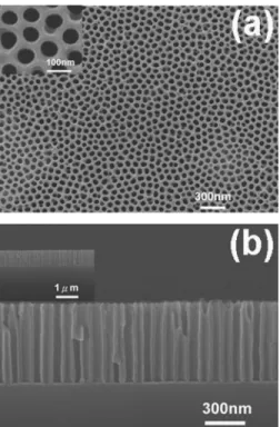
Figures 2共a兲 and 2共b兲 show the top-view and cross-sectional SEM images of the as-synthesized AAO before the CNT growth. Ordered pore channel arrays with pore size of 75 nm and pore-to-pore distance of 100 nm was observed on the substrates following the two-step anodization.15The as-pect ratio for the AAO channels is about 10. Figures3共a兲and
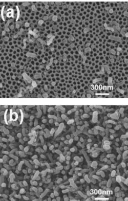
3共b兲show the morphology of the CNTs on the AAO template using recipe A in TableI. Initially, relatively few CNTs were observed in the pores of the AAO template with negligible entanglement among them. After 15 min of growth time, dense CNTs were present and its density共the ratio of filled pores兲 was estimated to be of 2.2⫻109tubes/ cm2共⬃28%兲.
Figure4shows a typical morphology for the CNTs grown on the blank Si wafer at 500 ° C for 15 min. Although the growth conditions were identical for both Figs. 3and4, the morphology of the CNTs grown on the blank Si substrate demonstrated substantial entanglements with density esti-mated at 6.5⫻1010tubes/ cm2.
The field-emission characteristics of the CNTs arrays on both substrates were examined with their results shown in Fig. 5. For AAO templated Si substrate, the electron emis-sion current density was found to attain 100 mA/ cm2under
an electric field of 8 V /m. In addition, the turn-on field, the electric field when the emission current density reaches 10A / cm2, was 2.8 V /m. In contrast, the electron emis-sion current density was merely 10 mA/ cm2 at the same electric field for blank Si wafer and its turn-on field was 4.5 V /m. The plotting of In共I/V2兲 vs 1/V, as shown in the inset of Fig. 5, could extract the slope. Following Fowler-Nordheim16共FN兲 relation, the field enhancement fac-tor were 2700 for AAO templated Si substrate whereas it was only 505 for blank Si wafer. This factor of 2700 was
TABLE I. Experiment conditions for the growth of CNTs.
Sample C2H4 flow rate 共SCCM兲 H2 flow rate 共SCCM兲 N2 flow rate 共SCCM兲 H2 pretreatment 共min兲 A 125 500 0 10 B 125 0 500 10 C 50 200 0 10 D 50 0 200 10 E 125 50 0 10 F 125 0 50 10
FIG. 1. Schematic diagram for the fabrication process of CNTs on an AAO template.
FIG. 2.共a兲 Top-view and 共b兲: cross-sectional SEM images of AAO template fabricated on a Si substrate.
104302-2 Yang, Chen, and Shieh J. Appl. Phys. 100, 104302共2006兲
the highest reported to date.5,6,17–19 Chen et al. also reported a similar field-emission current density with slightly higher CNT density of共6–8兲⫻109tubes/ cm2using AAO as a
tem-plate for CNT growth.18 Low screening effect among indi-vidual CNTs is likely to be responsible for the enhanced field-emission properties in this study. As clearly seen in Fig.
3, the filling ration of the CNTs was 28% and physical en-tanglements among them were minimized by AAO template. The field-emission properties for the CNTs arrays pre-pared by our approach are comparable to those obtained from CNTs derived from plasma enhanced growth. However, they are significantly better than those obtained by thermal CVD with precursor mixture in low hydrogen content, as listed on TableII. The uniqueness of our process enables us to grow CNTs at temperature as low as 500 ° C without the assistance of plasma. Although other types of quasi-one-dimensional objects such as carbon nanofibers共CNFs兲 were synthesized at certain low temperatures10,11,20 or even at
room temperature,7 their implementation especially for dis-play application is uncertain as field-emission efficiency data are lacking.
The VLS mechanism is often used to describe the cata-lytic growth of CNTs.9,11,21,22 The synthesis process should provide sufficient energy to produce molten catalytic par-ticles for subsequent alloying with impinging gaseous reac-tants. Carbon segregation at the bottom of the particle results in a stable graphitic structure.23As indicated, the minimum growth temperature for CNT formation in VLS model is given by the eutectic temperature of carbon and catalyst el-ement. Previous studies on SPD共Refs.7–9兲 process involved
catalytic synthesis of nanostructures such as CNFs,7,8 ZnSe,10 and GaAs 共Ref. 9兲 nanowires 共NWs兲 at relatively
low temperature. It was suggested that plasma7,8 and molecular-beam epitaxy10 共MBE兲 techniques were conduc-tive to facile diffusion of adsorbed reactants along the sur-face of catalyst particles. Generally, plasma is known to dis-sociate precursors,8 etch materials in amorphous phase on reacting surfaces,7as well as promote the diffusion capability of the reactive species.8,9These processes are recognized to benefit the SPD process.7–10 For example, Kamins et al.24 announced Ti-promoted Si NW growth at temperatures be-low the Si–Ti eutectic point by CVD method using the feed of excess precursors. In this study, the growth temperature was far below the C–Ni eutectic point of 1311 ° C.8Thus the growth mechanism is of particular interest. Previously, it was suggested that plasma heating and dissociative adsorption of hydrocarbon molecules would engender localized heating near the surface of the catalyst and cause surface melting at reduced growth temperature.25 Therefore, the VLS model may still be valid for our growth conditions. On the other hand, it is likely that SPD process might contribute to some degrees. However, the exact growth mechanism is not clear at this moment, and further study is necessary.
In our study, both the total flow rate and hydrogen ratio for the reacting precursor mixture are two to three times larger than those reported in other works.11,20–22Such a mix-ture not only allows for a steady supply of carbon atoms at the surface of the Ni particle but also promotes the
dissocia-FIG. 3. Top-view SEM images showing CNTs growth on AAO layers after 共a兲 10 min and 共b兲 15 min by a thermal CVD method at the temperature of 500 ° C using the recipe A in TableI.
FIG. 4. Plan-view SEM image for the CNTs morphology grown on the blank Si wafer at 500 ° C for 15 min.
FIG. 5. Field-emission characteristics of CNTs grown on AAO template and on blank wafers by a thermal CVD method using the recipe A in TableI. The inset shows FN plots for two curves shown on this figure.
tion of hydrocarbon reactants.22 Moreover, high hydrogen content enhances surface self-diffusion,26and removes amor-phous materials by hydrogen etching.24 These proposed ef-fects in our approach can be examined by varying the growth rate with temperature as performed before by Hofmann et
al.11,20 Figures 6共a兲–6共f兲show the cross-sectional SEM im-ages for the CNTs on blank Si substrate with the hydrogen flow for 15 min at 500, 550, 600, 650, 700, and 750 ° C, respectively. The length of the CNTs increases as the growth
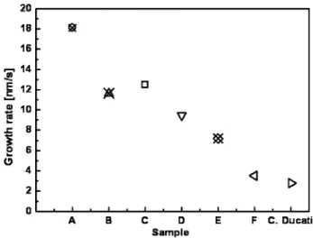
temperature was raised. Figure7compares the growth rate of the CNTs at 650 ° C for our samples A – F and the sample of Ducati et al.22 The growth conditions are listed in Table I. The growth rate of the CNTs grown on the blank Si substrate was about 18 nm/ s which is much higher than one obtained for thermal CVD共3.5 nm/s兲.22Base on the Arrhenius plot of growth rate versus reciprocal growth temperature 共1/T兲 as
TABLE II. Comparison of field-emission characteristics and parameters for CNT growth by our approach with those obtained by other research groups.
Temperature共°C兲 Dilution gas Field emission Reference
Thermal CVD
Ar⬍160 SCCM = 80– 5600
on AAO 550—900 Current density 5and6
H2⬍40 SCCM 24 mA/ cm2 N2⬍100 SCCM NH3⬍60 SCCM Ar⬍60 SCCM = 800– 7800 On blank 700–800 Current density H2⬍200 SCCM 100 mA/ cm2 15and17 N2⬍60 SCCM NH3⬍300 SCCM He⬍15 SCCM Plasma technique CVD = 1900– 2600
On AAO 600–660 H2= 2 – 80 SCCM Current density 18
100 mA/ cm2
H2= 2 – 270 SCCM = 3000 19and27 On
blank
280–700 CO2⬍30 SCCM Current density 19and27 173 mA/ cm2
N2= 2 – 100 SCCM
= 2700
Our work on AAO 500 H2= 500 SCCM Current density
100 mA/ cm2
FIG. 6. Cross-sectional SEM images showing the CNTs grown on the blank Si substrate for 15 min at various temperatures:共a兲 500 °C, 共b兲 550 °C, 共c兲 600 ° C,共d兲 650 °C, 共e兲 700 °C, and 共f兲 750 °C.
FIG. 7. Growth rate of CNTs on blank Si wafer by thermal CVD method at 650 ° C using various recipes listed on TableI. For comparison, the growth rate for CNTs grown by CVD with conventional recipes reported by Ducati et al. was also shown.
104302-4 Yang, Chen, and Shieh J. Appl. Phys. 100, 104302共2006兲
shown in Fig.8, activation energy EAfor our case with
pre-cursor with high hydrogen content was determined to be 0.55 eV. This value is slightly higher than 0.23 eV from the plasma synthesis route but much lower than 1.21 eV derived from standard thermal CVD.11,21 When hydrogen dilution was replaced with nitrogen dilution, the growth rate was re-duced by two times and the activation energy was increased to 1.02 eV. Decreasing either the total flow rate or hydrogen 共nitrogen兲 dilution also reduce the growth rate, as shown in Fig.7. Therefore we conclude that excess hydrogen dilution and abundant precursor inflow would initiate CNT growth at faster rate with possibly lower activation energy. As a result, we observe the CNT growth at relatively low temperature.
It is known that the growth rate of CNTs is nonlinear with respect to the growth duration. Evidence indicates that the growth rate tend to saturate after first 10– 20 min. To verify whether our growth rates were obtained before or after saturation, we measured the growth rates after 10 min using other sets of samples. TableIII共a兲 summarizes the height of
CNTs and corresponding growth rates for both 10 and 15 min growth time for C2H4: H2= 1 : 4. We found that the
growth rate measured at 15 min was faster than that mea-sured at 10 min, which indicates growth saturation was not attained after 15 min. The activation energy derived from the data measured at 10 min was 0.57 eV, which is close to 0.55 eV obtained at 15 min. Similarly for C2H4: N2= 1 : 4, no saturation on growth rate was observed up to 15 min as shown in Table III共b兲. The activation energy obtained from
the data at 10 min was 1.08 eV, which is quite close to 1.02 eV obtained at 15 min. Therefore, the activation energy we obtained using the data at 15 min should be reliable.
It is especially noted that we expect high hydrogen-diluted flow also enhances the transportation of reactants into the nanopores of the AAO template and the removal of amor-phous carbon on the top surfaces of the AAO template. In addition, it was reported that the AAO nanopores would pro-mote CNT growth.14 Therefore, the quality of CNTs was
further improved when they were grown on the AAO tem-plate even at a low temperature, a result suggested in Figs.2
and3.
IV. CONCLUSIONS
In conclusion, efficient field-emission CNT arrays on the AAO templated Si substrate was prepared at temperature as low as 500 ° C by a CVD method with hydrocarbon precur-sor in high hydrogen ambient. This approach enables suffi-cient reactants with high diffusivity, promotes dissociation of hydrocarbon reactants, as well as facilitates etching of amor-phous carbon by-products. Field-emission current density of 100 mA/ cm2at 8 V /m was measured. In addition, the ac-tivation energy for the CNT growth was determined to be 0.55 eV. We believe that high hydrogen content is beneficial to the VLS and SPD processes, which leads to relatively reduced growth temperature.
1C. Thelander, T. Mårtensson, M. T. Björk, B. J. Ohlsson, M. W. Larsson, L. R. Wallenberg, and L. Samuelson, Appl. Phys. Lett. 83, 2052共2003兲. 2N. G. Shang, F. Y. Meng, F. C. K. Au, Q. Li, C. S. Lee, I. Bello, and S. T.
Lee, Adv. Mater.共Weinheim, Ger.兲 14, 1308 共2002兲. 3Y. Xia et al., Adv. Mater.共Weinheim, Ger.兲 15, 353 共2003兲. 4A. T. Cho et al., Electrochem. Solid-State Lett. 8, G143共2005兲. 5H. Gao et al., J. Appl. Phys. 93, 5602共2003兲.
6S. M. Yoon, J. Chae, and J. S. Suh, Appl. Phys. Lett. 84, 825共2004兲. 7T. M. Minea, S. Point, A. Granier, and M. Touzeau, Appl. Phys. Lett. 85,
1244共2004兲.
8B. O. Boskovic, V. Stolojan, R. U. A. Khan, S. Haq, and S. R. P. Silva, Nat. Mater. 1, 165共2002兲.
9A. I. Persson, M. W. Larsson, S. Stenström, B. J. Ohlsson, L. Samuelson, and L. R. Wallenberg, Nat. Mater. 3, 677共2004兲.
10A. Colli et al., Appl. Phys. Lett. 86, 153103共2005兲.
11S. Hofmann, C. Ducati, J. Robertson, and B. Kleinsorge, Appl. Phys. Lett. 83, 135共2003兲.
12S. Sriraman, S. Agarwal, E. S. Aydil, and D. Maroudas, Nature共London兲 418, 62共2002兲.
13J. H. Wu, J. M. Shieh, B. T. Dai, and Y. C. S. Wu, Electrochem. Solid-State Lett. 7, G128共2004兲.
14A. M. Rao, D. Jacques, R. C. Haddon, W. Zhu, C. Bower, and S. Jin, Appl. Phys. Lett. 76, 3813共2000兲.
15E. J. Bae, W. B. Choi, K. S. Jeong, J. U. Chu, G. S. Park, S. Song, and I. K. Yoo, Adv. Mater.共Weinheim, Ger.兲 14, 277 共2002兲.
FIG. 8. Arrhenius plot of growth rate vs reciprocal growth temperature 共1/T兲 for high hydrogen 共nitrogen兲-diluted recipes. For comparison, the plot for CNTs grown by CVD with conventional recipes reported by Ducati et al. was also shown.
TABLE III. The height of CNTs and the corresponding growth rates mea-sured at 10 and 15 min.共a兲 C2H4: H2= 1 : 4 and共b兲 C2H4: N2= 1 : 4.
Growth time: 10 min Growth time: 15 min Growth Temp.共°C兲 CNT height 共nm兲 Growth rate 共nm/s兲 CNT height 共nm兲 Growth rate 共nm/s兲 共a兲 500 1 980 3.3 4 780 5.31 550 3 150 5.25 5 300 5.89 600 5 350 8.92 10 700 11.89 650 8 150 13.58 16 300 18.11 700 10 868 18.11 21 735 24.15 750 15 546 25.91 31 090 34.54 共b兲 500 213 0.35 426 0.47 550 750 1.25 2 330 2.59 600 1 580 2.63 6 010 6.68 650 3 550 5.92 10 470 11.63 700 6 270 10.45 14 980 16.64 750 11 950 19.92 19 680 21.87
16R. H. Fowler and L. W. Nordheim, Proc. R. Soc. London, Ser. A 119, 173 共1928兲.
17S. Wei, W. P. Kang, W. H. Hofmeister, J. L. Davidson, Y. M. Wong, and J. H. Hung, J. Vac. Sci. Technol. B 23, 793共2005兲.
18P. L. Chen, J. K. Chang, C. T. Kuo, and F. M. Pan, Diamond Relat. Mater. 13, 1949共2004兲.
19C. F. Chen, C. L. Lin, and C. M. Wang, Thin Solid Films 444, 64共2003兲. 20S. Hofmann, C. Ducati, B. Kleinsorge, and J. Robertson, Appl. Phys. Lett.
83, 4661共2003兲.
21S. Hofmann, G. Csányi, A. C. Ferrari, M. C. Payne, and J. Robertson, Phys. Rev. Lett. 95, 036101共2005兲.
22C. Ducati, I. Alexandrou, M. Chhowalla, G. A. J. Amaratunga, and J. Robertson, Appl. Phys. Lett. 92, 3299共2002兲.
23A. V. Melechko, V. I. Merkulov, T. E. Mcknight, M. A. Guillorn, K. L. Klein, D. H. Lowndes, and M. L. Simpson, J. Appl. Phys. 97, 041301 共2005兲.
24T. I. Kamins, R. S. Williams, D. P. Basile, T. Hesjedal, and J. S. Harris, J. Appl. Phys. 89, 1008共2001兲.
25V. Kayastha, Y. K. Yap, S. Dimovski, and Y. Gogotsi, Appl. Phys. Lett. 85, 3265共2004兲.
26S. Horch, H. T. Lorensen, S. Helveg, E. Lægsgaard, I. Stensgaard, K. W. Jacobsen, J. K. Nørskov, and F. Besenbacher, Nature共London兲 398, 134 共1999兲.
27W. H. Wang, Y. T. Lin, and C. T. Kuo, Diamond Relat. Mater. 14, 907 共2005兲.
104302-6 Yang, Chen, and Shieh J. Appl. Phys. 100, 104302共2006兲