摻氮及氮化鎵族奈米材料之光學特性
67
0
0
全文
(2) 摻氮及氮化鎵族奈米結構之光學特性 Optical Properties of Dilute Nitride-based and GaN-based Nanostructures. 研 究 生:蔡敏瑛. Student:Min-Ying Tsai. 指導教授:郭浩中教授. Advisor:Prof. Hao-Chung Kuo. 國 立 交 通 大 學 光 電 工 程 研 究 所 碩 士 論 文. A Thesis Submitted to Institute of Electro-Optical Engineering College of Electrical Engineering and Computer Science National Chiao Tung University in partial Fulfillment of the Requirements for the Degree of Master in Electro-Optical Engineering June 2005 Hsinchu, Taiwan, Republic of China. 中 華 民 國 九 十 四 年 六 月.
(3)
(4) 誌謝 碩士生涯歨入尾聲, 雖然這只是短短的兩年, 卻是影響我一生的重要時光。回憶這 兩年, 有歡樂也有悲傷, 有收穫也有失去, 在即將面對新生活的當下, 是我最好的寶 藏, 作為我迎向未來的後盾及解決問題的處方。在此, 我希望能將我的喜悅與感激的心 情, 與大家分享。 首先必須感謝指導教授郭浩中老師, 在他的指導及帶領下, 讓我在碩士兩年間走 向明確的研究方向, 並在我低潮及迷失時, 適時給予我鼓勵及支持。此外, 我還必須感 謝王興宗教授的悉心指導, 教授那份對研究的熱誠與執著, 深深的影響了我求學的態 度, 使我學習到做學問應有的態度及方法。 在求學的過程中, 實驗室張亞銜學長的帶領讓我對光學系統及儀器的架設有深入 的了解及認識, 在數據的分析與論文撰寫薛道鴻學長提供了許多寶貴的經驗以及指導, 而芳儀學姊總是能給予我寶貴的意見, 以及教導我正確的觀念; 王德宗學長在樣品的 提供, 游敏學妹在實驗上的協助, 讓我順利的完成研究; 並感謝學長蔡睿彥, 張詒安, 姚忻宏, 高志強, 朱榮堂, 張峻瑋和學姊妙佳, 在我遇到問題時, 不吝嗇給予我解答 與討論; 同學瑞溢, 文燈, 裕鈞, 永昌, 薏婷, 傳煜與國峰, 使我在實驗之外, 擁有 融洽相處的碩士生活, 充滿多采多姿的歡笑回憶; 另外, 還有碩一的學弟妹, 謝謝你 們的幫忙。 最後, 我要感謝我的家人, 總是在我背後鼓勵我支持我, 讓我沒有後顧之憂, 全 力面對眼前的一切。. i.
(5) 摻氮及氮化鎵族奈米結構之光學特性. 研究生: 蔡敏瑛. 指導教授: 郭浩中教授 國立交通大學光電工程研究所碩士班 摘要. 本論文中, 我們研究兩種以化學氣相沉積法成長之奈米結構樣品。採用光激發螢光 光譜及螢光激發光光譜進行一連串的光學特性研究。樣品依材質可區分為兩種類, 一是 一組由不同氮含量之氮砷化銦鎵/砷化鎵之單層量子井結構組成, 另一組則是改變長晶 條件所成長出一系列的氮化銦鎵量子點結構樣品。 透過不同氮含量之氮砷化銦鎵/砷化鎵之單層量子井樣品之光激發螢光光譜量測, 我們發現氮含量由 0%, 0.5%, 增加至 2%, 使得其光譜發生了與低氮含量樣本不同的行 為, 為了探討這樣差異的來源, 我們量測了變溫時光激發螢光之變化, 並仔細分析能 係變化與溫度的關係, 同時並測量出不同激發能量下之行為變化, 進而推論出摻雜之 氮含量至 2% 時, 此樣品具有類似於量子點之特性, 使得其光譜不像一般量子井結構容 易受到溫度的影響, 加上高解析度穿透式電子顯微鏡之影像輔助, 更確認了氮的摻入 不但造成空間上分布不均的局化態, 並形成近似於量子點結構之存在。 另外, 我們利用一種新方法成長了高密度之氮化銦鎵量子點樣品。在這個部分, 原 子力顯微鏡顯示出當我們改變了 SiNx 處理之時間, 可成長出一系列由小到大的量子點 結構, 其發光能隙具有紅移現象。透過光激發螢光光譜我們比較出不同大小量子點結構 發光能隙與溫度間的變化趨勢, 發現其對溫度的敏感度較低, 隨著溫度由 10K 增加到 300K,能隙變化最多只有 40 meV。 為獲得更多資訊, 我們進一步計算出其活化能之變化, 發現較小的量子點樣品相對於大量子點樣品具有較小的活化能, 其值約為只有大量子 點結構活化能之二分之一。同時在螢光激發光光譜的實驗中, 我們也觀察到大小量子點 間行為的差異。 ii.
(6) 最後我們選擇了一片氮化銦鎵量子點結構之樣品, 將其做快速熱退火, 觀察在不 同之熱退火溫度其發光能隙之變化。隨著退火溫度的增加, 快速熱退火對於我們的樣品 產生了影響, 造成波長的藍移現象, 並也使活化能減少, 這主要是由於銦或鎵的原子 由於熱而產生相互擴散而改變了樣本的能隙。. iii.
(7) Optical Properties of Dilute Nitride-based and Gallium Nitride-based nanostructures Student: Min-Ying Tsai. Advisor: Prof. Hao-Chung Kuo. Institute of Electro-Optical Engineering National Chiao Tung University Abstract In this thesis, two kinds of nanostructure samples grown by metalorganic chemical vapor deposition were studied. We utilized the photoluminescence (PL), photoluminescence excitation (PLE) to investigate the optical properties of our samples. The first series are In0.4Ga0.6As1-xNx/GaAs single quantum well structures with different nitrogen concentrations and the second ones are the InGaN/GaN quantum dots samples with different sizes. InGaAsN SQWs with various nitrogen concentrations, where x=0, 0.5 and 2%, were grown. on. GaAs. substrates.. The. effects. of. incorporating. nitrogen. into. the. In0.4Ga0.6As1-xNx/GaAs SQW were investigated using photoluminescence (PL) and high resolution transmission electron microscope (HRTEM).. In the case of In0.4Ga0.6As1-xNx. SQW with 2% nitrogen content, the PL emission from the quantum-dot-like states was observed and confirmed by the temperature- and excitation-dependent PL measurements. Detailed investigations conducted here indicate that the nitrogen not only influences carrier localization, but also is critical in the formation of quantum-dots. In the second part, we investigate the optical properties of ultra-high-density InGaN quantum dots (QDs). Atomic force microscopy revealed that the extremely high density about 3×1011 cm-2 of QDs was obtained and the size of QDs was increased with the duration of SiNx treatment. The PL-peak wavelength at 10K of the InGaN QDs samples is red-shifted as increasing the height of QDs. From the temperature dependence of the photoluminescence, the thermal activation energy (Ea) exhibited different activation energies for large and small QDs. Ea of the smaller QDs samples is about 59meV, much less than that of the largest QDs, iv.
(8) 122 meV. In addition, the PLE spectra broadened with increasing the height of QDs. Finally, we study the effects of rapid thermal annealing on optical properties of InGaN QDs with the SiNx treatment time. Their behaviors were investigated through temperaturedependent photoluminescence measurements. The results indicated that emission wavelength of the InGaN QDs shifted toward long wavelength after the post-thermal annealing, which may be due to In/Ga inter- diffusion and variation on the QDs size by post-grown thermal annealing.. v.
(9) Content 致謝...………………………………………………………………………………………….i 摘要………………………………………………………………………………………ii Abstract……………………………………………………………………………………iv Content…………………………………………………………………………………….vi List of Tables............………………………………………………………………….ix List of Figures……………………………………………………………………………..x Chapter I. Introduction…………………………………………………………….1. 1.1 Introduction…………………………………………………………………………...1 1.2 Motivation…………………………………………………………………………….2 Chapter II. Characteristic of III- Nitride Quantum Dot Structure………………….5. 2.1 The localized or quantum-dot like state in quantum well structure…………...5 2.2 The formation of quantum dot structure……………………………………………...5 2.3 Quantum confinement effects in quantum dots structure…………………………….7 Chapter III. Experimental Instrument and Setup…………………………………….11. 3.1 Optical Characterization…………………………………………………………….11 3.1.1. Photoluminescence (PL)………………………………………………...11. 3.1.2. Photoluminescence Excitation…………………………………………..12. 3.2 Structure Characterization…………………………………………………………..12 3.2.1. Atomic Force Microscopy………………………………………………12. 3.2.2. Transmission Electron Microscopy……………………………………13. 3.3 Post-grown Rapid Thermal Annealer……………………………………………….13 3.4 Experiment setup…………………………………………………………………….14 3.4.1. Long wavelength u-PL setup……………………………………………14. 3.4.2. PL setup………………………………………………………………….14. 3.4.3. PLE setup………………………………………………………………..15 vi.
(10) Chapter IV. Optical and structural properties of InGaAsN Single Quantum Well…...19. 4.1 Introduction………………………………………………………………………….19 4.2 Sample preparation………………………………………………………………….19 4.3 Optical properties of InGaAsN single quantum well……………………………….20 4.3.1. Temperature dependence of photoluminescence………………………..20. 4.3.2. The evolution of the PL emission energy with temperature…………….21. 4.3.3. The excitation-power dependent PL…………………………………….22. 4.3.4. Internal quantum efficiency excitation of sample C…………………….22. 4.4 TEM morphology of samples……………………………………………………….23 4.5 Conclusion…………………………………………………………………………..23 Chapter V. Structural and Optical properties of InGaN Quantum dots…………..31. 5.1 Introduction………………………………………………………………………….31 5.2 Sample preparation………………………………………………………………….31 5.3 Surface morphology of un-capped samples…………………………………………32 5.4 Optical properties of InGaN QDs…………………………………………………...32 5.4.1. Photoluminescence spectra with different quantum dot sizes…………..32. 5.4.2. Temperature dependence of photoluminescence spectra………………..33. 5.4.3. The activation energy for different size quantum dots…………………..34. 5.4.4. Photoluminescence excitation spectra…………………………………..34. 5.5 Conclusion…………………………………………………………………………..35 Chapter VI. Annealing effects in InGaN quantum dots………………………………41. 6.1 Introduction………………………………………………………………………….41 6.2 sample preparation…………………………………………………………………..41 6.3 Optical properties of InGaN QDs with different annealing temperature……………42 6.3.1. Power dependence of photoluminescence………………………………42. 6.3.2. PL spectra for three samples at room temperature………………………42 vii.
(11) 6.3.3. Temperature dependence of photoluminescence………………………..43. 6.4 Conclusion…………………………………………………………………………..43 Chapter VII Conclusion and Future Work…………………………………………….47 7.1 Conclusion…………………………………………………………………………..47 7.2 Future work………………………………………………………………………….48 Reference……………………………………………………………………………………..49. viii.
(12) List of Tables Table I : The summary for the InGaN QD samples of growth condition we prepared. Table II : Table II: The characteristics of InGaN QDs as-grown and annealed samples.. ix.
(13) List of Figures Fig. 1.1.1: The relation between dimension and density of states. Fig. 1.2.1: A brief history of research on QD lasers particularly at the initial stage. Fig. 2.2.1: The diagram of strain relaxation for S-K growth mode. Fig. 2.2.2: A SEM bird’s-eye-view and cross-sectional view of InGaN QD structures Fig. 2.3.1: The carrier behavior in three dimension confinement structure. Fig. 2.3.2: The scheme of the calculated transition energy for QDs with different sizes.. Fig. 3.2.1: The working principle of AFM. Fig. 3.2.2: A technical explanation of the typical TEMs. Fig. 3.4.1: Long wavelength µ-PL setup Fig. 3.4.2: PL setup Fig. 3.4 3: PLE setup Fig. 4.2.1: The structure diagram of In0.4Ga0.6As1-xNx shown here. Fig. 4.3.1: The temperature dependent of the PL spectra of (a)sample A(In0.4Ga0.6As/GaAs SQW), (b)sample B (In0.4Ga0.6As0.995N0.005/GaAs SQW ) and (c) sample C (In0.4Ga0.6As0.98N0.02/GaAs SQW) Fig. 4.3.2: Evolution with the temperature of the PL-peak energies for the (a)sample A(In0.4Ga0.6As/GaAs SQW), (b)sample B (In0.4Ga0.6As0.995N0.005/GaAs SQW ) and (c) sample C (In0.4Ga0.6As0.98N0.02/GaAs SQW) Fig. 4.3.3: Excitation-power dependent PL of (a) sample B (In0.4Ga0.6As0.995N0.005/GaAs SQW ) and (b) sample C (In0.4Ga0.6As0.98N0.02/GaAs SQW). Fig. 4.3.4: Temperature dependency of the PL integrated intensity of the sample C (In0.4Ga0.6As0.98N0.02/GaAs SQW) under different excitation conditions. Fig. 4.4.1: High-resolution TEM images of (a) sample B (In0.4Ga0.6As0.995N0.005/GaAs SQW ) and (b) sample C (In0.4Ga0.6As0.98N0.02/GaAs SQW). Fig. 5.2.1: The InGaN QD sample structure (a) un-capped sample for AFM measurement (b) x.
(14) full sample structure for optical measurement. Fig. 5.3.1: 1µmx1µm AFM images of InGaN layers with (a) 2 min, (b) 2min 40 sec, (c) 3min15 sec of SiNx treatment on the underlying GaN layers. Fig. 5.4.1: Normalized PL spectra at 10K for samples 2min, 2min 40 sec, and 3min15sec, respectively. Fig. 5.4.2: The diagram of the transition levels for different size QDs. Fig. 5.4.3: The PL peak energy positions of the quantum dots as a fuction of the temperature, which are normalized to the same at 10K. Fig. 5.4.4: Arrhenius plot of normalized PL intensity as a function of tem-perature samples 2min, 2min 40sec, and 3min 15sec. Fig. 5.4.5: PL and PLE spectra are demonstrated for diff erent sizes QDs. Fig.6.2.1: Surface morphology of the as-grown InGaN QDs scanned by AFM measurement. Fig. 6.3.1: Power dependent PL for Sample A. Fig.6.3.2: Normalized PL spectra from samples A, B, and C measured at RT. Fig.6.3.3: Arrhenius plots of the temperature dependent of the integrated PL for three samples.. xi.
(15) Chapter I Introduction 1.1 Introduction In recent years, the Related III-V nitride materials were the most extensively investigated and would be used for the promising optical devices in the next generation, especially for light emitting diodes (LEDs) and laser diodes (LDs). However, the quantum confined effects causing by low dimension structure would bring the devices more effective properties such as operating in low threshold current, higher direct modulation speed, and reducing the temperature sensitivity. According to the different dimension and density of states on the semiconductor materials, we can separate them into four groups including three-dimensional (3-D) structure of bulk material, 2-D structure of quantum well (QW), 1-D structure of nanowire/ nanorod/ nanopillar, and 0-D structure of quantum dot (QD), shown as Figure 1.1.1. A 3D system has the density of states of a parabolic shape. With decreasing the dimension of sample structure to 2D structure, the density of state is made up of a pile of step functions. Then, the density of states in a 1D diverges at En and finally the spectra of 0D systems reflect the δ–function shape of the density of states. The best-known examples of semiconductor structure with reduced dimensions are the quantum well structures, which are made of alternating layers of two kind semiconductors with different bandgap energy, for example, InGaN/GaN system. But, in InGaN/GaN quantum well system, large compositional fluctuation of In in InGaN/GaN QWs due to a large difference in the lattice constants between GaN and InN causes a different behavior. Many results show that the origin of strong emission from InGaN/GaN quantum wells can be attributed to exciton localization in the quantum dot-like region [1]. The behavior of this quantum dot-like structure is an important issue in QW structure. However, in InGaAs system, the InGaAs1-xNx material lattice-match to GaAs and its large band offset were attractive as the active region material for the fiber communication. When the Nitrogen content in InGaAs is increased, the behaviors which are different from the InGaAs QWs would be also observed, which could be due to the formation of localization nanostructure in quantum wells. But, the mechanism is not very clear yet. Regarding quantum dot structures which dimensions are lower than quantum wells, their unique optical and electronic characteristics due to atomic-like discrete states with a δ–function density of states, higher luminescence efficiency, and modified carrier recombination lifetime are investigated by many groups and attract more attentions. Within the last decade, there has been a lot of research devoted to realizing the predicted behavior of 1.
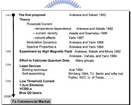
(16) zero-dimensional (0-D) nanostructures. In 1982, the first concept of the QDs was proposed as artificial atoms for semiconductor laser applications by Arakawa and Sakaki [2]. They proposed the semiconductor laser with a QD active region promises many profound effects on various improvements, including ultra low and temperature independent threshold current [2, 3], high-frequency modulation with negligible chirping effect [4], high- temperature operation, and nonlinear gain effect [5]. By the end of the 1980s, the fabrication of QDs by lithographic patterning and etching QW structure was considered main techniques to fabricate QDs. The crystal growth on a bulk substrate occurs in one of three distinct modes, Frank-vander Merwe (FM), Volmer-Weber (VW), and Stranski–Krastanow (SK). While growth proceeds layer by layer in the FM mode, VW growth causes three-dimensional islands on the substrate, if the film has a higher surface energy than that of the substrate. SK growth is a combination of the FM and VW modes, where the growth of a several-monolayer thin film, called a wetting layer, is followed by cluster nucleation and then to island formation. The growth of InAs on lattice mismatched GaAs layer was first found to form three-dimensional (3-D) nanoscale islands on top of a thin InAs wetting layer by CNET in 1985. Stranski–Krastanow (S–K) growth mode is formed with the strain-driven process when the misfit is larger than 1.7% [6]. The details of how to grow the samples by S-K growth mode will be introduced in the next chapter. On the other hand, we will also introduce another self-assembling growth named antisurfactant method, which is what we focus on in this study in chapter V and VI. By 1995, this self-assembling growth for making nanoscale islands led to a breakthrough to QD devices such as lasers and detectors for both interband and intersubband transitions. Self-assembling growth is a convenient method to obtain QDs because any patterning is not needed. In the contrast, the position of the QDs can not be controlled and the QDs are randomly distributed. Although the merit of selective growth is useful to control QDs, the way of forming QDs is not easy and convenient because of the complicated progress. Fig. 1.2.1 shows a brief history of research on QD lasers particularly at the initial stage until 1999 [6].. 1.2 Motivation of this study For InGaAsN system, the behavior of the single quantum well structure with different Nitrogen contents is not understood well. And the quality of self-assembled QDs, including the uniformity, shape, and size, remains to be improved by trying and tuning the different parameters or growth methods to optimize. In this thesis, we investigated the structural and 2.
(17) optical properties for different samples including InGaAsN single quantum wells and InGaN quantum dots with different sizes. In order to understand the special behavior in dilute nitride materials and in QDs structure, we carried out temperature dependent photoluminescence and low temperature photoluminescence excitation to analysis the behavior of those nanostructures in various materials. However, the theoretical calculation of band offset values in InGaN system is simply performed and compared with experimental results. Besides, for InGaN QD samples, we also investigate the effect of rapid thermal annealing with different annealing temperatures. The organization of this thesis is as following: Chapter II discusses the different method to form the QD samples and theoretical background. The experimental principle and setup are described in chapter III. Detailed behaviors expected for InGaAsN single quantum well structures are obtained in chapter IV. The experimental results of InGaN QD for different sizes and the effect of rapid thermal annealing are discussed in chapter V and VI, respectively. Finally, the summary of this study is presented in chapter VII.. 3.
(18) 3 -D. 2 -D. D(E). E. Fig. 1.1.1: The relation between dimension and density of states. Fig. 1.2.1: A brief history of research on QD lasers particularly at the initial stage.. 4.
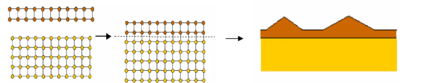
(19) Chapter II Characteristic of III- Nitride nanostructure 2.1 The localized or quantum-dot like state in quantum well structure The behaviors of localization or quantum-dot like state were investigated well in InGaN quantum well with high Indium content [1]. In that study, the results showed that the origin of strong emission from InGaN/GaN quantum wells can be attributed to exciton localization in the quantum dot-like region. In InGaAs system, therefore, the origin of quantum-dot like states in the quantum well is not well understood, and there are relatively few reports on InGaAsN/GaAs QDs [7-11]. The present results show the experimental evidence of the 3D growth mode in the sample with high nitrogen content. This phenomenon most likely occurs due to the influence of various nitrogen contents on growth model transition, i.e., 2D to 3D growth to minimize the free energy while increasing nitrogen contents. Moreover, theoretical studies have shown that island formation is results from the competition between strain relaxation and surface energy [12]. A crucial factor in the control of 3D island growth is the lattice mismatch among the island material, underlying substrate and the surrounding matrix.. The lattice mismatch. between the InGaAs and GaAs substrate is known to be able to be varied by adjusting the nitrogen contents, and therefore offers a range of compressive strains [13, 14]. The introduction of nitrogen into a highly compressive strain system can reduce the average strain; on the other hand, the local strain around N atom may increase owing to the smaller nitrogen atom radius compared to arsenic.. The effect of this local strain may enhance the 3D growth. mode. Therefore, the mechanism is not confirmed by strong evidences. Furthermore, Herrera et al. proposed that the introduction of N could be responsible for the enhanced phase separation [10]. The presence of phase separation could also locally reduce the energy barrier for the transformation into stable 3D islands.. 2.2 The formation of quantum dot structure There are three main methods to form the quantum dot structure including Stranski–Krastanow (S–K) growth mode, antisurfactant method, and selective method. We summarize the growth methods in recent years and introduce below: (i). Stranski–Krastanow (S–K) growth mode (layer-then-island). The evolution of an initially two-dimensional growth in to a three-dimensional growth front is a well-known phenomenon and has been frequently observed in various systems. This growth mode is used by various materials grown under compressive stress on heterostructure by strain-driven quantum dot formation during heteroepitaxy as a bottom-up 5.
(20) approach. After deposition of a few two-dimension monolayers (MLs), island structures are self-formed on a 2D wetting layer as a result of the transition of the growth mode and the three-dimension occurs because lattices mismatch between interfaces and the stress needs to be released, as shown in Fig. 2.2.1. The strain relaxation mechanisms would be first published by Stranski and Krastanow and we called the growth mode as S-K growth mode. Especially, S-K growth has been successfully demonstrated to form self-assembled quantum dot (SAQD) on large area substrate with a good throughput and compatibility to current microelectronic technology [15]. (ii). Antisurfactant method. Using this growth way, the surfactant is believed to play an important role in changing the surface free energy of the samples. We can use the unequal equation to show the surface free energy in three- dimension growth mode in a system, δs<δf+δi ,. Eq. (2.1.1). where δs is the surface free energies of substrate, δf shows the surface free energies of film, and δi represents the surface free energies of interface between substrate and film. As a third element like the surfactant is added, the sign of the unequal equation would be change by altering the substrate surface free energy [16]. Using this growth method, the surfactant is believed to play an important role in changing the surface free energy of the material. Some reports have shown the similar reversed effect occurs in GaN-based system [16, 17]. The antisurfactant is believed to inhibit the film growth and intentionally modify the two-dimension mode into three-dimension mode. However, the role of the antisurfactant is still unknown in the enhancement of island growth, Therefore, carrying out the basic mechanism in growth way would be important to us for further detailed studies. In this thesis, the chapter V would be focused on the growth way of antisurfactant method using the SiNx as an antisurfactant. This is different from many other groups. (iii). Selective method. Self-assembling growth is a convenient method to get QDs but the position of the QDs is difficult to be controlled. Using selective method to obtain QDs, in the contrast, the shape, size, and position of the QDs could be artificially designed and controlled. In general, the selective method can control the position of the QDs by the methods of focused ion-beam irradiation and photo-assisted wet chemical etching. S. Sakai, et al. [18] grew the QDs on Si-patterned GaN/sapphire substrates. We could use different patterns to grow QDs in different shapes. Here, we simply introduce the InGaN QDs formation by selective method published by Y. Arakawa, et al. [5]. In this paper, after depositing three 6.
(21) periods of InGaN MQWs on the grid-like SiO2-GaN-sapphire patterned substrates, they believe that InGaN QD structures are formed at the tops of the hexagonal pyramids. Figure 2.2.2 show a SEM bird’s-eye-view and cross-sectional view of InGaN QDs structures. Shown as Fig. 2.2.2(b), no material was deposited on the SiO2 mask and the positions of the QDs were controlled very well.. 2.3 Quantum confinement effects in nanostructure Regarding nanostructures such as quantum dot-like nanostructure or quantum dot structure, their unique optical and electronic characteristics due to atomic-like discrete states with a δ–function density of states, higher luminescence efficiency, and modified carrier recombination lifetime are investigated by many groups. Within the last decade, there has been a lot of research devoted to realizing the predicted behavior of zero-dimensional (0-D) quantum-confined structures. For low-dimensional structures, in spite of the fact that the size of the confinement is larger than the exciton Bohr radius, it is known that a compression of the exciton, and thus a change in the exciton binding energy occurs. In a quantum dot, the electronic states are quantized and the energy levels become discrete. In Figure 2.3.1, we could see the carriers are localized in the quantum dot structure for three dimension confinement. Because of the localization of carriers trapped at QDs structure where the energy separation between the ground and the first higher exciton state is larger than the thermal energy kBT, the lifetime of the 0-D exciton strongly is almost independent of temperature [19]. Knowing the quantum dot size and the ratio of the dot radius to the exciton Bohr radius in the bulk material, we could calculate the difference of electron and hole sub-bands between two materials to determine the energy gap. The quantum dots which we consider in general have the small ratio of thickness to diameter. Therefore, the energy shift in those structures is due to quantization in the longitudinal direction. The k․p model is used to calculate the interaction matrices of our nanostructures under stain. Shown as the Fig. 2.3.2, in the strong confinement regime, i.e., in small size QDs, where the sub-band energy separations are much larger than the electron-hole Coulomb interaction of the exciton binding energy, the exciton ground state is mainly composed of the lowest-energy sub-band [15]. As the quantum dot size is increased, the energy levels of the quantized sub-band become smaller. Finally, in the week-confinement regime where the quantum dot size is much larger than the exciton Bohr radius, the quantized sub-bands are 7.
(22) distributed almost continuously and the binding energy is nearly the same as in the bulk material. Compared to the calculation results, the shift in the energy level due to the three-dimensional quantization could be found from photoluminescence measurements. The detail analysis would be discussed below.. 8.
(23) Fig. 2.2.1: The diagram of strain relaxation for S-K growth mode. Fig. 2.2.2: a SEM bird’s-eye-view and cross-sectional view of InGaN QD structures. 9.
(24) Fig. 2.3.1: The carrier behavior in three dimension confinement structure.. Large QD. Small QD e2 e1. e1. e1-hh1. e1-hh1. e1-lh1. e1-lh1. hh1 hh2 hh1. lh1 hh3. lh1. lh2. Fig. 2.3.2: The scheme of the calculated transition energy for QDs with different sizes.. 10.
(25) Chapter III Experimental Instrument and Setup 3.1 Optical Characterization Optical characterization is contactless, nondestructive method of probing the initial behavior of materials and structures with minimal sample preparation. Specifically, light is directed onto a sample, where it is absorbed and imparts excess energy into the material in a process called photo-excitation. One way this excess energy can be dissipated by the sample is through the emission of light, or luminescence. In the case of photo-excitation, this luminescence is called photoluminescence. The intensity and spectral content of this photoluminescence is a direct measure of various important material properties.. 3.1.1 Photoluminescence (PL) Photoluminescence is the emission of light from a material under optical excitation. The energy of the laser light should be large than the band gap energy of the semiconductor in order to get all information. The exciting light is absorbed in the semiconductor and will produce electrons in the conduction band and a hole in the valence band. When an excited electron in an excited state returns to the initial state forming a photon whose energy is the difference between the excited state and the initial state energies, then we detect the PL signal. In order to restore the equilibrium, the electrons and holes will combine in many ways. Those processes can be direct or indirect depending on the gap energy of the material. The PL spectra are obtained by analyzing the spectral elements of the emitted light. At low temperature, there are different possibilities of recombination. An electron and a hole can pair together and form a Free Exciton (FE), normally referred to a Wannier-Mott exciton [20]. This exciton is characterized by a high mobility and comparably low binding energy. The FE may move freely in the lattice until it recombines radiatively or non-radiatively or until it encounters a defect. At the defect, FE exciton forms a Bound Exciton (BE) because of loosing some of energy. Some applications of photoluminescence are bandgap determination, impurity levels and defect detection, recombination mechanisms and material quality, showed as below: •. Band gap determination. The most common radiative transition in semiconductors is known as the band gap which is the difference between the conduction and valence bands. Band gap determination is a particularly useful and basic process when working with new compound semiconductors.. 11.
(26) •. Material quality. Non-radiative processes are usually associated with localized defect, whose existence will decrease material quality and device performance. Therefore, material quality can be detected by analyzing the amount of radiative recombination.. •. Recombination mechanisms. Recombination known the return to equilibrium can involve both radiative and non-radiative processes. The amount of photoluminescence and its dependence on the level of photo-excitation and temperature are directly related to the dominant recombination process. According to analyzing of photoluminescence, we could understand the physical mechanism of the recombination.. •. Impurity levels and defect detection. Radiative transitions in semiconductors are also related to localized defect states. The photoluminescence energy associated with these different levels could identify specific defects in materials, and the intensity of photoluminescence can be used to determine their qualities of structures.. The article below discusses how photoluminescence can be used to analyze the optical properties of III-V nitride QD structure materials.. 3.1.2 Photoluminescence Excitation In PL measurement, which is performed at fixed excitation energy, the luminescence properties are generally investigated. While PL excitation (PLE) spectroscopy, which is carried out at fixed detection energy, provides mainly information about the absorption properties. Apart from absorption and PL experiments, the PLE measurement is a widely used spectroscopic tool for the characterization of optical transitions in semiconductors. It is also very important to note that the PLE also depends strongly on the different carrier relaxation processes that connect the absorbing state to the luminescent state. For example, it is possible to recognize the absorption in a quantum well (QW) from that of the substrate if they have different emission energies, in which because it can be assumed that carrier transfer between substrate and QW is negligible. Nevertheless, in many cases it is difficult to separate the influence of relaxation from that of absorption. The PLE spectrum is strongly influenced by the relaxation depending on different samples.. 3.2 Structure Characterization 3.2.1 Atomic Force Microscopy Atomic force microscopy images the surface of a sample by scanning a sharp tip over it 12.
(27) and measuring the deflection of the tip. The working principle is illustrated in Figure 3.2.1. A piezoelectric scanner moves the sample in the x-y direction under the tip. The position of the tip is measured by reflecting a laser from the backside of the cantilever to a split photodiode. Depending on the distance between the tip and the sample so that the force acting on the tip is repulsive, the AFM work in contact mode. In non-contact or tapping mode the tip is further away from the sample and in the regime of an attractive force [21]. The cantilever is set to vibrations close to its resonant frequency and changes in the surface morphology lead to changes in the frequency, which can be measured sensitively. The change in the frequency is used as a feedback. The AFM used in our experiments was called Large Sample Scanning Probe Microscope named Digital Instruments DI 5000.. 3.2.2 Transmission Electron Microscopy (TEM) A TEM works much like a slide projector. A projector shines a beam of light through (transmits) the slide, as the light passes through it is affected by the structures and objects on the slide. These effects result in only certain parts of the light beam being transmitted through certain parts of the slide. This transmitted beam is then projected onto the viewing screen, forming an enlarged image of the slide. TEMs work the same way except that they shine a beam of electrons (like the light) through the specimen (like the slide). Whatever part is transmitted is projected onto a phosphor screen for the user to see. A technical explanation of the typical TEMs is showed as figure 3.2.2[22]. High-resolution TEM (HRTEM) images could provide structural information at better than 0.2 nm spatial resolution. In most crystalline inorganic materials, including ceramics, semiconductors and metals, the positions of individual atomic columns can be resolved, at least in low-index zones. When recorded under optimum conditions, electron micrographs can be directly interpreted in terms of the projected crystal potential. For highest resolution, specimens must be <10nm thick. In general, specimens prepared by chemical thinning, crushing, or ion beam milling will contain suitable regions [23]. 3.3 Post-grown Rapid Thermal Annealer The RTA system we used here to investigate the post-grown thermal annealing effect is heatpulse 610i rapid thermal processing system. The RTA temperature range is from 400oC~1250oC and the duration of maximum time up to 300 seconds.. 3.4 Experiment setup 13.
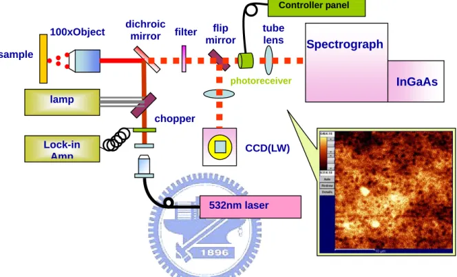
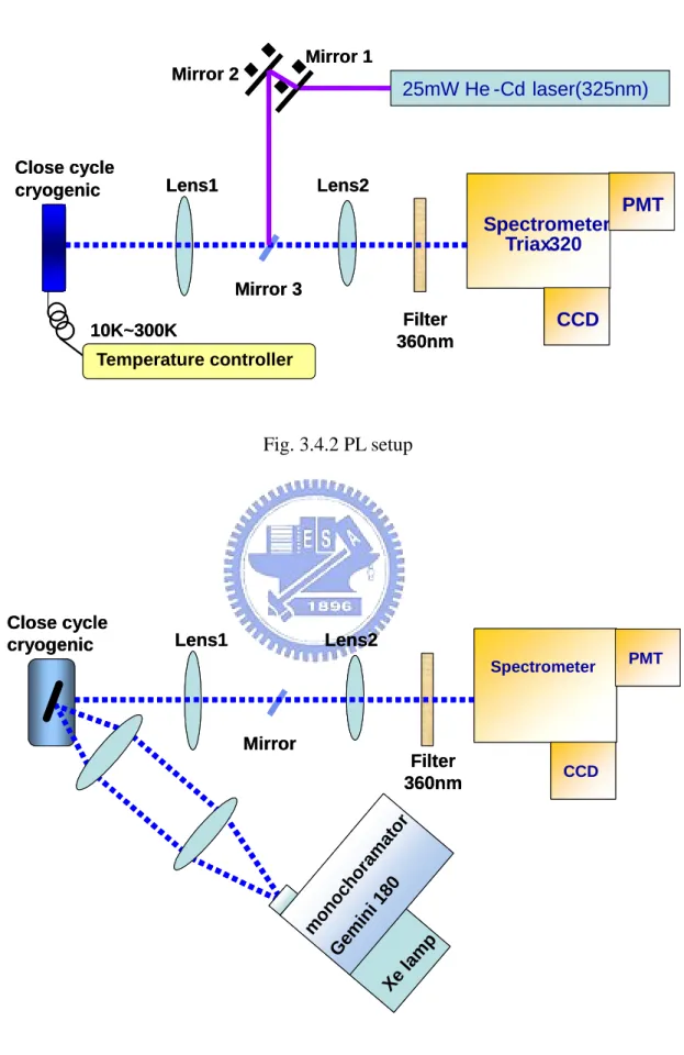
(28) 3.4.1 Long wavelength µ-PL setup The PL of long wavelength samples was excited by the 532 nm line of an Ar+-ion laser. Before the luminescence light excited by laser in focused on the input slit of the monochromator, a long pass filter was set to filter out the stray laser. Adding gray filters enabled the light to be attenuated by various factors. Using the 100x objective here, the light from the lasers can be focused on a spot with a minimum diameter of 3 µm on the sample. All samples were placed in a closed-cycle cryostat with a temperature controller ranging from 10 K to room temperature. Furthermore, the luminescence was dispersed with a 320 mm monochromator (Jobin-Yvon Triax 320) and detected by a thermo-electrically (TE) cooled InGaAs detector. The signal of luminescence was recorded by the lock-in amplifier using phase-loch technique, which was introduced for amplified the modulated signal amplitude. The wavelength resolution was about 1nm by using 300 grooves/mm grating and the slit of 0.1 mm. On the other hand, we also set up a system to scam the confocal image, shown as Fig. 3.4.1. Such a confocal optical system enables the highly spatial resolution beyond the diffraction limit of a light wave. We could detect the surface inhomogeneous and/or PL surface emission of our samples.. 3.4.2 PL setup The schematic system setup of PL system is shown in Fig. 3.4.2. The pumping light source was a multi-mode and non-polarized Helium-Cadmium laser operated on 325 nm with 20 mW. After reflecting by three mirrors, the laser light was focused by a lens, which focal length was 5 cm, to 0.3 mm in diameter and the luminescence signal was collected by the same lens. The probed light was dispersed by 0.32 m monochromator ( Jobin-Yvon Triax-320) equipped with 1800, 1200, and 300 grooves/mm grating and which maximum width of the entrance slits was 1 mm. For my case, I chose to use the 300 grooves/mm grating and the slit of 0.1 mm. Under these conditions, the wavelength resolution was approximately 1 nm. In order to prevent the stray laser light from the sample surface passing through the detector, I also used long pass filter with a cut-off wavelength of 360 nm in front of the entrance slit to get real spectra without combining the scattering pumping laser. Eventually, for GaN-based materials, the probed light was detected by the charge couple device (CCD). All samples were placed in a closed-cycle cryostat with a temperature controller ranging from 10 K to room temperature.. 14.
(29) 3.4.3 PLE setup Except the excited source, the light collection system and spectrometer (Triax 320) were almost the same as PL setup. As shown in Fig. 3.4.3, the sample was mounted in a closed cycle helium refrigerator cooled down to 10K. The pumping source called Xe lamp with 450 W was separated by double-grating monochoramator (Jobin-Yvon Gemini 180) and then coupled to the samples at an angle about 45o by two focal lenses. We fixed the detection energy of the spectrometer Triax 320, and changed the excitation energy of Xe lamp from 300nm to the band gap of each sample. At the exit of the spectrometer Triax 320, a high sensitive Hamamatsu photomultiplier tube (PMT) with GaAs photocathode was placed to detect the luminescence signals.. 15.
(30) Fig. 3.2.1. The working principle of AFM. Fig. 3.2.2. A technical explanation of the typical TEMs. 16.
(31) Controller panel. 100xObject. dichroic flip mirror filter mirror. tube lens. sample. Spectrograph. photoreceiver. lamp chopper Lock-in Amp. CCD(LW). 532nm laser. Fig. 3.4.1. Long wavelength u-PL setup. 17. InGaAs.
(32) Mirror 1 Mirror 2. Close cycle cryogenic. 25mW He -Cd laser(325nm). Lens2. Lens1. Spectrograph. PMT. Spectrometer Triax320 Mirror 3 Filter 360nm. 10K~300K. CCD. Temperature controller. Fig. 3.4.2 PL setup. Lens2. Lens1. Spectrograph Spectrometer. Mirror. 18 0. p la m Xe. G em. in i. oc ho. ra m. at or. Filter 360nm. m on. Close cycle cryogenic. Fig. 3.4.3.PLE setup. 18. CCD. PMT.
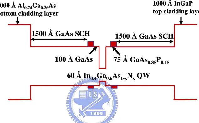
(33) Chapter IV Optical and structural properties of InGaAsN Single Quantum Well 4.1 Introduction Long wavelength vertical cavity surface-emitting lasers (VCSELs) are essential devices for light source in optical fiber metropolitan-area networks (MAN) [24]. However, the lasing wavelength of most InGaAsN-based lasers has been limited to around 1.3 µm, due to difficulty in growing high-quality InGaAsN/GaAs QW structures with high composition of In or N.. First, higher indium composition increases the compressive strain to a critical point at. which the structural quality of the layer undulation of the interfaces begins to show plastic relaxation;[25] Second, alloying N into the InGaAs QW has proven challenging owing to the low efficiency of N incorporation combined with a large alloy miscibility gap in the phase diagram [26,27].. Furthermore, larger N and In concentrations broaden the luminescence. linewidth of the alloys, increase the non-radiative (monomolecular and Auger) recombination and thus reduce the material gain and increase transparency carrier density [28,29,30]. Recently, Chang et al. found that incorporating nitrogen content exceeding 0.7% in InGaAsN significantly reduced the laser characteristics and temperature of laser performance [28]. Therefore, understanding the influence of nitrogen in InGaAsN is especially valuable. This study examines how nitrogen incorporation influences optical properties including the carrier localization and material properties of In0.4Ga0.6As1-xNx/GaAs SQW with x=0, 0.5 and 2 %. Photoluminescence (PL), and high resolution transmission electron microscope (HRTEM) measurements are performed for understanding the crystal and the interface quality of InGaAsN-GaAs.. Finally, quantum-dot-like behavior is observed in In0.4Ga0.6As0.98N0.02. via the temperature- and excitation-dependent PL measurements as well as HRTEM.. 4.2 Sample preparation All samples investigated were grown by low pressure metalorganic chemical vapor deposition (LP-MOCVD). The AsH3 and PH3 as hydride sources were supplied as the group-V precursors, the trimethyl precursors of gallium (Ga), aluminum (Al), and indium (In) acted as the group-III precursors, and the N precursor was U-dimethylhydrazine. The active regions were all based on a 60 Å In0.4Ga0.6As1-xNx QW sandwiched between GaAs (100 Å)-GaAsP (75 Å) materials. A diagram of the structure is shown in Fig. 4.2.1. Moreover, the In and N contents of the InGaAsN material were determined via PL, X-ray diffraction and secondary ion mass spectrometry. The details of growth conditions have been published elsewhere [31-33]. The values of the N composition x in the structures was 0, 0.5 and 2 % for samples A, B and C, respectively. 19.
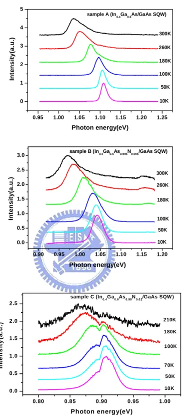
(34) The surface morphology of the sample was determined by optical microscopy and atomic force microscopy (AFM). Roughness analysis indicated that smooth and mirror-like surfaces (on the nanoscale), which are exactly like that of a GaAs homoepitaxial layer, can be achieved under optimized growth conditions. Cross-sectional TEM thin foils were prepared through mechanical polishing followed by argon-ion milling.. 4.3 Optical properties of InGaAsN single quantum well To estimate the nitrogen and indium concentration dependence of the band gap, this study adopted the band anticrossing (BAC) model proposed by Sham et al [12]. The theoretical model based on a BAC model interaction between the highly localized nitrogen-derived state and the zone-center conduction band Bloch states has been constructed and applied to explain the band-gap behavior, including pressure and temperature dependence, for bulk dilute nitrides including GaNAs, GaInNAs, and GaNP.. However, the extent to. which this model accurately describes the underlying physics of this new class of material remains unclear.. According to the model, the band gap of InGaAsN can be expressed as. E g ( Inx Ga1− x As1− y N y ) 2 ( x, y ) EM ( x) + E N − [ EM ( x) − E N ]2 + 4VNM , = 2. Eq. (4.3.1). where the top of the valence band serves as a reference energy level, EM is the extended conduction band of the InGaAs ternary compound, EN is an impurity level due to nitrogen incorporation, which is assumed here to be located 1.65 eV above the valence band, and VNM represents the degree of interaction between the EN and EM levels [34]. The band gap energies of samples A, B and C, calculated using Eq. (4.3.1), provide a reference.. 4.3.1 Temperature dependence of photoluminescence The temperature dependence of the PL spectra of samples A, B and C is shown in Fig. 4.3.1. The variation of peak position with temperature can be attributed to the effect of the extension of the lattice and electron lattice interaction. Figure 4.3.1(a) clearly shows that only one mainly symmetrical emission peak centered about 1.10 eV was observed when the temperature was below 90 K.. Sample B exhibited extremely similar behavior to sample A. except for the reduction of the band-gap energy because of increasing N content. Remarkable broadening of the full width at half maximum (FWHM) is obvious in samples A and B.. The inhomogeneous and temperature-dependent homogenous parts are known to. 20.
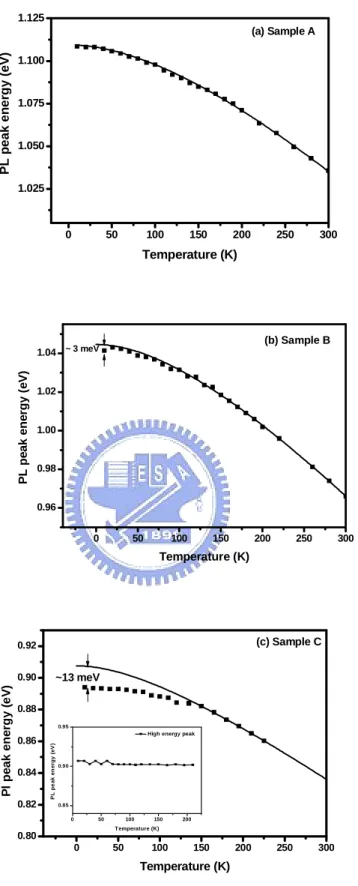
(35) contribute to the luminescence broadening [35]. Furthermore, the value of homogeneous broadening, based on the assumption of excitonic luminescence, is considerably smaller than the values obtained experimentally for samples A and B.. This comparison indicates that. most of the broadening of the PL-peaks might be inhomogeneous in origin, owing to interface roughness and random alloy disorder. from samples A and B.. Notably, the luminescence feature of sample C differs. Apparently, unlike those of the symmetric low-temperature PL. spectra observed in samples A and B, the most striking feature in sample C was that another peak appears at the high-energy side.. The origin of the extraordinary peak at high-energy. side will be discussed later.. 4.3.2 The evolution of the PL emission energy with temperature Figure 4.3.2 shows the evolution with temperature of the energy of PL peak for the three samples investigated here.. The solid lines represent the fitting results in the. high-temperature range using the empirical Varshni model [36] E (T ) = E (0) −. αT 2 , T +β. Eq. (4.3.2). where the α and β are Varshni parameters, and T denotes the measured temperature. The carrier localization energy at any temperature is obtained as Eloc (T ) = E (T ) − E PL (T ) , where EPL(T) denotes the temperature dependence of the PL peak energy[37]. Figure 4.3.2 illustrates the temperature dependence of the PL emission energies and the Varshni fit of the three samples. Figure 4.3.2(a) indicated that the PL-peak position for the sample A is in agreement with the regular thermalization of the carriers.. The localization energies of samples B and C at 10. K are also given in Fig. 4.3.2. The figure showed that N content influenced the carrier localization in the investigated QW systems.. Additionally, obviously the linewidth increases. accordingly when the temperature increases above 10 K. The incorporation of nitrogen into the InGaAs is reported to increase the density of defects originating from compositional and structural inhomogeneities, and reduces the crystalline quality [38, 39].. Increasing nitrogen. content thus will increase the localization energy of carriers in QWs. This dependence agrees with our observations on localization energy of samples A and B.. The band tail states. in the density of states originating from the high density of defects are responsible for the so-called S-shaped temperature dependence of emission energy of InGaAsN QWs [40]. Moreover, Grenouillet et al. and Pinault et al. discussed the S-shape, and explained it by 21.
(36) carrier localization at low temperatures [37, 41].. However, the S-shape does not appear in. the case of InGaAs quantum wells, and is less pronounced in GaAsN quantum wells. Pronounced S-shape features were not manifested in the present samples, a phenomenon which might be owing to the insufficient nitrogen concentration (or better crystalline quality) [42].. Figure 4.3.2(c) displays the temperature-dependent emission peaks observed on the. low-energy side of sample C.. Additionally, the emission peak at high-energy side (inset of. Fig. 4.3.2(c)) did not exhibit significant changes when the temperature was increased above 10 K.. 4.3.3 The excitation-power dependent PL To explore the mechanism of temperature-insensitivity of sample C, as mentioned above, excitation-power dependent PL was performed on all samples, and the spectra are shown in Fig. 4.3.3. Figure 4.3.3(a) presents a series of spectra recorded at various excitation powers for sample B.. A clear tendency of blueshift with increasing excitation power which is can be. observed. Besides, both samples A and B exhibit very similar behavior of excitation-power dependent PL except for the centre of the emission wavelength.. As shown in Fig. 4.3.3(b). for sample C, only one peak appears under low excitation power, just as in samples A and B. However, one peak appears on the high-energy side with increasing excitation power, starting as a shoulder under an excitation power of 4 mW, and then becomes a clean peak at 0.9 eV under an excitation power of 8 mW.. Finally, this extra peak at high-energy side becomes. dominant over the initial peak under low excitation power.. This phenomenon most likely. the feature of quantum dots (QDs) resulting from carrier localization and a more efficient recombination through QDs, which has been observed in other III-nitride semiconductor alloys [43]. Furthermore, the extra peak also displays temperature insensitivity, as shown in Fig. 4.3.2(C). The trends of both temperature insensitivity and increase in the intensity with excitation power reveals that the extraordinary peak on the high energy-side of PL emission observed in sample C could be inferred to possibly originate from the quantum-dots-like states. The high emission energy of 0.9 eV band might due to the quantum-confined induced shift while the persistent of the high energy peak with temperature can be understood by the less electron-phonon interaction in the dots-like structure. Nevertheless, the intensity of the high energy peak decreases faster with temperature than the low energy peak and the high energy shoulder of the 0.9 eV band shrunk with 22.
(37) temperature. This thermal quenching behavior of high energy peak of sample C might be attributed to trapped excitons or carriers thermalizing from localized regions resulting from potential fluctuation in QD-like states. Further increase in temperature degrades the PL intensity is caused by the recombination of the thermally activated carriers with the non-radiative mechanism in the sample.. 4.3.4 Internal quantum efficiency excitation of sample C The temperature dependency of the PL integrated intensity of the sample C under different excitation conditions is plotted in Fig. 4.3.4 to demonstrate the internal quantum efficiency. Generally, the internal quantum efficiency can be evaluated by the temperature dependence of the integrated PL intensity [43, 44]. The figure clearly shows that the internal quantum efficiency, under low excitation, rapidly decreases with increasing temperature.. In. contrast, the internal quantum efficiency under high excitation decreases slowly with increasing temperature.. The high internal quantum efficiency is though to possibly result. from the quantum-dot like states under high excitation power, leading to more efficient recombination.. Similar results have also been observed in the InGaN/GaN MQWs [43].. 4.4 HRTEM morphology of samples Figure 4.4.1 shows the high resolution TEM image of the In0.4Ga0.6As1-xNx SQW. A very clear interface of In0.4Ga0.6As0.995N0.005 SQW was obtained on the atomic-layer lever (Fig. 4.4.1(a)), whereas no dislocations were observed in low magnification images.. Many. studies have reported that a suitable amount of nitrogen incorporation to InGaAs can reduce the net strain [27, 45]. Additionally, the HRTEM image of sample B shows very high crystallinity without extended structural defects, which resembles that of conventional III-V materials. Notably, for sample C with 2 % nitrogen content (In0.4Ga0.6As0.98N0.02 SQW), small dark regions with a size of about 2~3 nm were formed in the interface, as shown in Fig. 4.4.1(b), implying the existence of the quantum-dot like states.. Additionally, the rough. interface indicates reduced material quality, which is consistent with the observation of significantly reduced PL intensity from the lower signal-to-noise ratio and measurable temperature.. 4.5 Conclusion This study has investigated the temperature- and excitation-dependent PL spectra with high-resolution transmission electronic microscopy measurements on In0.4Ga0.6As1-xNx SQW 23.
(38) grown by MOCVD (x=0, 0.5 and 2 %). The evolution of the PL-peak position shows evidence that the carrier localization occurs in InGaAsN SQW with high N content (> 0.5%), and the localization energy changes depending on the N content.. Structural investigation by. HRTEM indicated that the In0.4Ga0.6As0.995N0.005 SQW possesses extremely high crystallinity and, moreover, lacks extended structural defects. For the In0.4Ga0.6As1-xNx SQW with 2% nitrogen content, strong emission from quantum-dot-like states has been observed, confirmed by the temperature- and excitation-dependent PL measurements.. Additionally, the superior. internal quantum efficiency under high excitation compared to that under low excitation demonstrates that the emission mechanism under high excitation might be dominated by quantum-dot-like behavior.. The present experimental results indicate that the nitrogen not. only influences carrier localization, but also is critical to the formation of QDs. further studies are required to clearly identify the mechanisms suggested above.. 24. However,.
(39) 1000 Å InGaP top cladding layer. 1000 Å Al0.74Ga0.26As bottom cladding layer. 1500 Å GaAs SCH. 1500 Å GaAs SCH. 100 Å GaAs. 75 Å GaAs0.85P0.15. 60 Å In0.4Ga0.6As1-xNx QW. Fig. 4.2.1. The structure of diagram is shown here. 25.
(40) 5 sample A (In0.4Ga0.6As/GaAs SQW). 4. Intensity(a.u.). 300K. 3. 260K 180K. 2. 100K. 1. 50K 10K. 0 0.95. 1.00. 1.05. 1.10. 1.15. 1.20. 1.25. Photon energy(eV). sample B (In0.4Ga0.6As0.995N0.005/GaAs SQW). 3.0. Intensity(a.u.). 2.5. 300K. 2.0. 260K. 1.5. 180K. 1.0 100K. 0.5. 50K. 0.0. 10K. 0.90. 0.95. 1.00. 1.05. 1.10. 1.15. 1.20. Photon energy(eV). sample C (In 0.4 Ga 0.6 As 0 .98 N 0.0 2 /GaAs SQW ). Intensity(a.u.). 2.5 210K. 2.0. 180K. 1.5 100K. 1.0 70K. 0.5. 50K 10K. 0.0 0.80. 0.85. 0.90. 0.95. 1.00. Photon energy(eV). Fig. 4.3.1 The temperature dependent of the PL spectra of (a)sample A(In0.4Ga0.6As/GaAs SQW), (b)sample B (In0.4Ga0.6As0.995N0.005/GaAs SQW ) and (c) sample C (In0.4Ga0.6As0.98N0.02/GaAs SQW). 26.
(41) 1.125. PL peak energy (eV). (a) Sample A 1.100. 1.075. 1.050. 1.025. 0. 50. 100. 150. 200. 250. 300. Temperature (K). (b) Sample B. PL peak energy (eV). 1.04 ~ 3 meV. 1.02. 1.00. 0.98. 0.96 0. 50. 100. 150. 200. 250. 300. Temperature (K). (c) Sample C. 0.92. ~13 meV. 0.88 0.95. 0.86 0.84 0.82. High energy peak PL peak energy (eV). Pl peak energy (eV). 0.90. 0.90. 0.85 0. 50. 100. 150. 200. Temperature (K). 0.80 0. 50. 100. 150. 200. 250. 300. Temperature (K). Fig. 4.3.2. Evolution with the temperature of the PL-peak energies for the (a)sample A(In0.4Ga0.6As/GaAs SQW), (b)sample B (In0.4Ga0.6As0.995N0.005/GaAs SQW ) and (c) sample C (In0.4Ga0.6As0.98N0.02/GaAs SQW) 27.
(42) (a) sample B 4. Intensity ( a.u.). 15mW 13.7mW. 3. 12mW 10mW 8mW. 2. 4mW 2mW 1mW. 1. 0.8mW 0.4mW 0.2mW 0.1mW. 0 0.90. 0.95. 1.00. 1.05. 1.10. 1.15. 1.20. Photon energy (eV). 4.0. (b) sample C 3.5. Intensity ( a.u.). 3.0 2.5. 13.7mW 8mW. 2.0 4mW. 1.5. 2mW 1mW. 1.0 0.5. 0.8mW 0.5mW 0.2mW 0.1mW. 0.80. 0.85. 0.90. 0.95. 1.00. Photon energy (eV). Fig.4.3.3. Excitation-power dependent PL of (a) sample B (In0.4Ga0.6As0.995N0.005/GaAs SQW ) and (b) sample C (In0.4Ga0.6As0.98N0.02/GaAs SQW).. 28.
(43) Internal quantum efficency (%). 100. low excitation high excitation. 80 60 40 20. Sample C 0 0.00. 0.02. 0.04. 0.06. 0.08. 0.10. 1/T (1/K). Fig.4.3.4 Temperature dependency of the PL integrated intensity of the sample C (In0.4Ga0.6As0.98N0.02/GaAs SQW) under different excitation conditions.. 29.
(44) (a). (b). Fig.4.4.1. High-resolution TEM images of (a) sample B (In0.4Ga0.6As0.995N0.005/GaAs SQW ) and (b) sample C (In0.4Ga0.6As0.98N0.02/GaAs SQW).. 30.
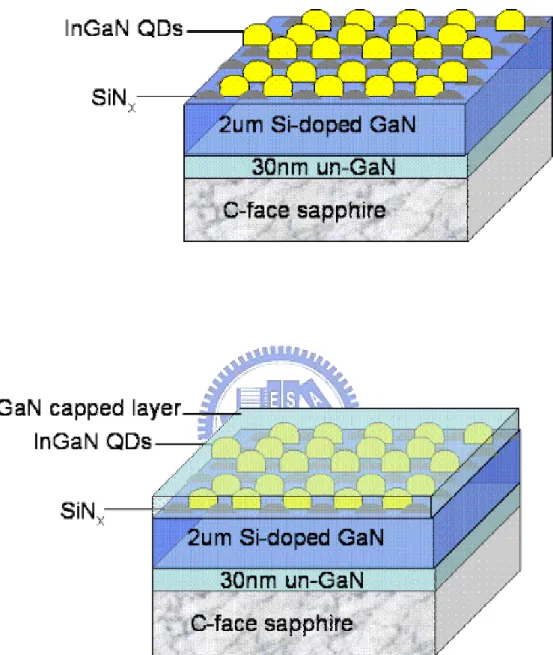
(45) Chapter V Structural and Optical properties of InGaN QDs with different sizes 5.1 Introduction Currently, GaN and related materials are the subjects of intense research due to their applications in laser diodes (LDs) and light-emitting diodes (LEDs) that operate between the ultraviolet and the visible regions. InGaN/GaN quantum wells (QWs) structures have successfully been used as the active layers in LEDs and LDs [46]. Having quantum dots (QDs) instead of QWs as the active layer is expected to improve the performance of LDs. LDs with QD structures in the active layer have been theoretically predicted to have superior characteristics, including lower threshold currents and narrow spectra [47]. Moreover, because of the localization of carriers trapped at dislocations, QD structures have been expected to increase the efficiency of the luminescence of LDs [48]. To ensure suitability for QDs laser applications, QDs layers with high spatial density and of uniform size must be grown [49]. Several approaches have been investigated for fabricating InGaN QDs, including the Stranski-Krastanow growth mode [50, 51] and growth using anti-surfactant [52, 53]. This study investigates the optical property, the surface morphology and the density of InGaN QDs following different durations of SiNx treatment on the underlying GaN layer before the InGaN layers were deposited. InGaN QDs with a very high density of near 3× 1011cm-2 and strong photoluminescence (PL) intensity were obtained. The relationship between the average size and the activation energy of InGaN QDs is also addressed. And photoluminescence excitation (PLE) for different size QDs is demonstrated, too.. 5.2 Sample preparation Three InGaN QD samples were grown on c-face sapphire substrates by metalorganic vapor phase epitaxy (MOVPE) with undergoing treatment durations of different SiNx to form different size or shape quantum dots [54-56]. The sample structures are showed in the Figure 5.2.1(a). A 300 Å-thick low-temperature GaN nucleation layer was first grown at 550oC on sapphire. Then, the reactor temperature was increased to 1000oC to grow a 2 µm-thick underlying Si-doped GaN underlying layer, providing a step- flow grown surface as confirmed by atomic force microscopy (AFM). Then, a rough SiNx layer with different treatment durations was grown on the n-type GaN underlying layer. In my study, I chose three different durations which were 2min, 2min 40sec, and 3min 15sec to treat my SiNx layers. During the treatment of the SiNx layer, the flow rates of NH3 and the diluted Si2H6 were 5 slm and 50 sccm, respectively. The temperature was then ramped down to 800oC to grow the 31.
(46) InxGa1-xN layers. As soon as the InGaN layers deposition was complete, the growth temperature was reduced to room temperature. During the growth of the InGaN layers, the vapor phase ratio TMIn/(TMIn+TEGa) was fixed at 0.35. The detail growth procedures were given otherwise [57]. In the other hand, I also prepared three other samples that additional 10 nm un-doped GaN layers were grown to investigate the optical property of the InGaN QD structure. The sample structure with the un-doped GaN capped layer was showed in Figure 5.2.1(b). Here, the three capped samples of 2min, 2min 40sec, and 3min 15sec treatment durations are labeled QD-200, QD-240, and QD-315, respectively. The detailed growth conditions of InGaN samples that had undergone various durations of SiNx treatment were examined, as listed in Table I. 5.3 Surface morphology of un-capped samples The surface morphology of all samples grown was characterized by AFM. Scans were performed over a surface area of 500 nm, using a Digital Instruments Nanoscope with a sharpened Si3N4 tip. In Fig. 5.3.1, AFM images of the uncapped samples QD-200, QD-240 and QD-315 are showed. The AFM images were performed over a surface area of 1µmx1µm. The average lateral size and thickness of the QD-200 are about 33.2 nm and 1.09 nm. As increasing the duration of treatment, the QD sizes become larger, 1.19 nm height and 35.2 nm width for QD-240 sample. For QD-315 sample, the average height is up to 2.66 nm and the lateral size is almost the same as former. The densities of different size QDs were estimated to increase approximately from 2.1×1011cm-2 to 2.9×1011cm-2. The Ultra high density is much larger than the dislocation density. This means that the main parts of the QDs are free of defects. This is useful for achieving high efficiency emission.. 5.4 Optical properties of InGaN QDs 5.4.1 Photoluminescence spectra with different quantum dot sizes The optical characteristics of the InGaN QDs samples were first evaluated with a 20mW HeCd laser operated at 325 nm. Figure 5.4.1 shows the corresponding normalized PL spectra at 10K for samples QD-200, QD-240 and QD-315. The dominant peak wavelengths for each spectrum are 428nm (2.900eV), 433nm (2.869eV) and 448nm (2.767eV), respectively, which clearly show a red-shift with the duration of SiNx treatment. The red-shift could be attributed to decreasing the QDs sizes or changing shapes due to quantum confined effects of low dimension structure [58]. In order to confirm our experiment results, energy states in QDs were simply solved by self-consistent Schrödinger equation. We used cylindrical symmetric 32.
(47) coordinate to describe our QD structure and then only calculated the half of the QD to demonstrate the whole behavior. As demonstrated in Fig. 5.4.2, the sample with smaller QDs size has larger e1-hh1 emission energy, which is 2.947 eV in calculation, than the larger ones (2.724eV). The result that the PL-peak wavelength of the larger QDs is longer is confirmed by theoretic calculation.. 5.4.2 Temperature dependence of photoluminescence spectra In order to observe the tendency of energy gap as temperature change, the PL peak-energy of the QDs recorded at different temperature for the three samples is showed in Fig. 5.4.3. When the lattice temperature of the QDs was increased from 10 K, a gradual shift of the PL peak to lower energy occurred. The peaks of all samples at 10K were normalized to zero. The PL position, before normalization peak positions were 2.900, 2.869, and 2.767 eV for QD-200, QD-240, and QD-315, respectively. For QD-200 and Sample-240, the total peak-energy shifts of around 10 meV were observed in the temperature range of 10-300 K in Figure 5.4.3, and these shifts are obviously lower than that of bulk GaN (80 meV) [59] and InGaN/GaN MQW (54 meV) [58, 60]. With increasing the duration of treatment time, the behavior of the larger InGaN QDs which shift is about 40meV is larger than that of the smaller QD samples. We could use Varshni equation [36], as followed, to fit the curve of QD-315 on the change of energy gap with temperature increasing.. αT 2 Eg (T ) = Eg (0) − β +T. Eq. (5.4.1). It is well known that the red-shift of the band-gap energy originates from the interaction with phonon. The smaller red-shift observed for QD structures can be explained by partial decoupling of the phonon-exciton interaction of the QDs [61, 62]. The phonon coupling clearly decreases with QD size decreasing. Therefore, a direct consequence of the decreased phonon coupling is the smaller redshift of the PL peak with increasing temperature [59]. Besides, the emission peaks of QD-200 and QD-240 showed clearly the “S-shaped” emission shift behavior below 200K. This could be explained by a carrier localization effect at low temperature. The blue-shift results from the confinement- induced shift of the electronic levels, whereas the red-shift results from the increased Coulomb energy induced by a compression of the exciton Bohr radius. In alloy in-homogeneity and/or In phase separation have been proposed as the origin of the localized states [63]. It reveals different potential fluctuations 33.
(48) within these two samples compared with a larger size of high-density QDs.. 5.4.3 The activation energy for different size quantum dots To further study the dimensional property of the QD structures, figure 5.4.4 shows the normalized PL intensity as a function of temperature for samples QD-200, QD-240, and QD-315. The experimental data were fitted by using Arrhenius equation based on the band tail model suggested by Eliseev et al. as follow [64],. I 1 = I 0 1 + A exp(− Ea ) kT. Eq. (5.4.2). The thermal activation energy, Ea, can be estimated to be about 59 meV, 60 meV and 122 meV from the data. In the high temperature range, we could find two main different activation energies between the large and small QDs. For QD-200 and QD-240 samples, their Ea about 60 meV are much less than the Ea of QD-315, which is about 122meV. The activation energy of the small QDs which is lower than that of the large QDs is attributed to serious quantum-confined effect [65, 66]. In other words, the larger Ea in the small QDs reflects that the ground state of the transition energy is closer the barrier height. For QD-315 sample compared with the QD-200 and QD-240 samples, we calculated the small difference between the GaN barriers and InGaN QDs. The 618meV of the conduction-band offset and the 412meV of the valence-band offset are evaluated for large QDs and small QDs, respectively. We suggest the activation energy of our InGaN QDs samples are incompletely caused by the holes escape from the QDs into the GaN barriers. This lower activation energy compared with theoretical calculation might be related to the quenching due to strong quantum-confined effect and the defect states formed at the InGaN/GaN interface and/or dislocations in the wetting layer.. 5.4.4 Photoluminescence excitation spectra We also carried out the PL and PLE spectra to investigate the action with different QD sizes at 10K. PLE measurements were performed using the dispersed light from the Xe lamp with the continuous radiation. As shown in Fig. 5.4.5, we observed the three different PLE spectra as changing the detection energy from 2.767 eV to 2.9 eV. For the QD-315 sample, the broaden band tail spectrum was obtained. The PLE spectra broaden and the PL peak energy show pronounced red-shift with 34.
(49) increasing the height of QDs, as showed in Fig. 5.4.5. From PLE spectra at 10K, a sharp peak is observed at about 3.5eV for each sample, which is the signal of GaN barrier. The near-band-age emissions from InGaN QDs are 2.91, 2.87, 2.78 eV for the samples of QD-200, QD-240, QD-315, respectively. With increasing the QD size, the broader and smoother PLE spectrum was observed. We also found there are some weak absorption edges in the small QD samples, which may be caused by small potential fluctuations in the sample [67].. 5.5 Conclusion In conclusion, we have investigated the optical properties of ultra-high-density InGaN quantum dots (QDs) grown by MOCVD. Atomic force microscopy revealed that the extremely high density about 3×1011 cm-2 of QDs was obtained and the size of QDs was increased with the duration of SiNx treatment. The PL-peak wavelength at 10K of the InGaN QDs samples is red-shifted as increasing the height of QDs. Moreover, the PL peak position with arising temperature for different sizes of QDs was found that the larger size of QDs revealed obviously red-shifted behavior. From the temperature dependence of the photoluminescence, the thermal activation energy Ea could be found two main different trends between the large and small QD samples. The Ea of the smaller QDs samples about 60 meV is half of that of the largest QD sample. This lower activation energy compared with theoretical calculation might be related to the quenching due to strong quantum-confined effect and the defect states formed at the InGaN/GaN interface and/or dislocations in the wetting layer. In addition, the PLE spectrum of the larger QD sample is broader and smoother than that of smaller ones.. 35.
(50) Fig. 5.2.1. The InGaN QD sample structure (a) un-capped sample for AFM measurement (b) full sample structure for optical measurement.. 36.
數據


+7
相關文件
Nonreciprocal Phenomena in Chiral Materials - Left and Right in Quantum Dynamics –..
• Atomic, molecular, and optical systems provide powerful platforms to explore topological physics. • Ultracold gases are good for exploring many-particle and
In x 2 we describe a top-down construction approach for which prototype charge- qubit devices have been successfully fabricated (Dzurak et al. Array sites are de ned by
* Anomaly is intrinsically QUANTUM effect Chiral anomaly is a fundamental aspect of QFT with chiral fermions.
To explore different e-learning resources and strategies that can be used to successfully develop the language skills of students with special educational needs in the
Explore different e-learning resources and strategies that can be used to successfully develop the language skills of students with special educational needs in the..
To help students achieve the curriculum aims and objectives, schools should feel free to vary the organization and teaching sequence of learning elements. In practice, most
Schools implementing small class teaching may have different sizes of grouping and different numbers of groups subject to the learning objectives and students’ needs.. The number
