A 1-V CMOS VCO For 60-GHz Applications
Tang-Nian Luo, Shuen-Yin Bai, Yi-Jan Emery Chen, Hsin-Shu Chen, and Deukhyoun Heo* Graduate Institute of Electronics Engineering, Department of Electrical Engineering
National Taiwan University, Taipei, Taiwan E-mail : [email protected]
* School of Electrical Engineering and Computer Science Washington State University, Pullman, WA 99164, USA Abstract—An integrated 1-V, 50-GHz CMOS
voltage-controlled-oscillator (VCO) is presented for the emerging 60-GHz UWB applications. Implemented in a commercial 0.18µm CMOS technology, the core VCO circuitry consumes 4mW of power and occupies only 90µm×120µm of the silicon estate. The high quality-factor line inductors and NMOS varactors are used to construct the LC-resonators. The measured phase noise at 1-MHz offset from 49 GHz is -96 dBc/Hz, which leads to an excellent Figure-of-Merit (FOM) of -184 dBc/Hz.
I. INTRODUCTION
The successful deployment of the various communication services stimulates the investigation of more usable bandwidth at higher frequency spectrum. Recently the RFIC designed for 60-GHz applications has attracted growing interest worldwide because of the availability of the unlicensed 7-GHz bandwidth and numerous obvious opportunities. Many applications require or benefit from high data rate communication, such as the high quality home video transmission which requires the data rate exceeding 1 Gb/s [1]. The wireless LAN at 2.4 or 5 GHz can obviously not meet this kind of transmission requirement. In addition, the signals at 60 GHz are prone to be absorbed by walls and floors, and are less likely to interfere with the signals far away. Therefore, it is very suitable for pico-cell high-data rate wireless communications.
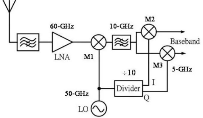
Fig. 1 shows the proposed double-conversion zero-IF wireless receiver architecture for the 60-GHz applications. A high-pass filter is placed between the antenna and the low-noise amplifier (LNA) to reject the lower-sideband image components of the first-stage down-conversion. The local oscillator (LO) frequency of the first-stage down-converter is 50 GHz and the IF frequency is 10 GHz. The first-stage IF signal goes through a band-pass filter to get rid of the harmonics and feeds into the even-harmonic mixers. By use of the even-harmonic mixer, the dc-offset issue from the self-mixing of the LO leakage can be alleviated. The quadrature LO signals of the even-harmonic mixers can be generated by dividing the first-stage LO signal.
Accordingly, the oncoming communication devices need to be supported by the affordable semiconductor technology. Because of the advantages of the semi-insulating substrate and high electron mobility, the microwave and millimeter-wave integrated circuits are traditionally implemented in III-V compound semiconductor technology. However, with the successful scaling following the Moore’s Law, CMOS technology becomes the potential contender for the implementation of MMIC although the lossy Si substrate and the low Q (quality factor) on-chip passive components still remain the main design challenges. Several CMOS VCOs oscillating above 40 GHz have been demonstrated recently [2]-[9]. To work around the lossy Si substrate, some VCOs are implemented in high-resistive-substrate or SOI CMOS technology to enhance the oscillation frequency, fmax, of the
transistor and Q of the inductors [5]-[7]. The push-push technique is adapted to the CMOS technology for building the harmonic oscillators and relaxing the speed requirement of the transistors in the circuits [8]-[9].
This paper presents an integrated 1-V, 50-GHz CMOS VCO for the 60-GHz wireless receiver. The VCO is implemented in the commercial 0.18µm CMOS technology of which the maximum transistor cut-off frequency, fT, is 60
GHz. Although the CMOS transistors in this VCO are biased far below the quiescent current attaining the maximum fT to
Figure 1. 60-GHz wireless receiver front-end architecture.
comply with the low power paradigm, a high
f
oscf
T peak_ ratio of 0.83 is achieved. To the authors’ knowledge, the low power and low phase noise of the VCO result in the excellent FOM of -184 dBc/Hz, which is best of the CMOS millimeter-wave fundamental VCOs published so far.Figure 2. Schematic diagram of the CMOS VCO.
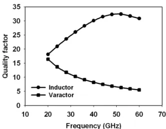
Figure 3. Simulated Q of the line inductor and NMOS varactor.
II. VCO CIRCUIT DESIGN
The VCO circuit consists of the NMOS cross-coupled transistor pair, line inductors, and the NMOS varactors, as shown in Fig. 2. The cross-coupled NMOS transistor pair (M1-M2) results in the negative resistance to compensate the resistance of the resonant tanks and meet the oscillation conditions. The oscillating frequency is determined by the tank inductance, varactor capacitance, and parasitic capacitance.
The design of the resonant tanks is closely related to the phase noise and power consumption of the VCO. Revisiting the Leeson’s oscillator phase noise model [10], the phase noise is inversely proportional to the square of the loaded Q of the tank. In addition, the lower the resistance of the tank, the lower the bias current needed to initiate the oscillation. Therefore, the characteristic of the resonant tanks is crucial to the performance of the VCO. The LC tanks consist of line inductors and NMOS transistors functioning as varactors. The line inductors have been reported to be applicable for MMIC design and able to offer some advantages of size and characteristics over microstrip or CPW transmission lines in Si-based IC technology [11]. The 2µm-thick-Al inductor metal is used to implement the line inductors, and their length and width are 50 µm and 15 µm, respectively. The
simulated Q of the line inductors, using ADS Momentum, is more than 30 at 50 GHz as shown in Fig. 3.
Figure 4. VCO die photograph.
The NMOS transistors are used as the varactors in the tunable resonant tanks. The NMOS varactor is implemented by connecting the drain and source of the NMOS transistor together and operating the MOS capacitor in the depletion and inversion regions. To reduce the resistance of the induced bottom-conduction-layer and polysilicon gate, and hence improve the Q of the varactor, the minimum gate length of the NMOS transistor is selected. The gate width of a single MOS capacitor is 2.5µm and four capacitor fingers are interconnected in parallel by metal to further reduce the resistance. The simulated Q of the NMOS varactor, also shown in Fig. 3, is about 7 at 50 GHz. The resonant frequency of the LC tanks is much higher than the VCO oscillation frequency because the parasitic capacitance surpasses by far the varactor capacitance.
III. MEASUEMENT RESULTS
The die photograph of the CMOS VCO is shown in Fig. 4. The area of the VCO core circuit is only 90µm×120µm. An Agilent E4407B 26.5GHz spectrum analyzer and 11970Q (33GHz-50GHz) external harmonic mixer are used for measurement. The VCO operates on a 1-V power supply and dissipates the minimum power of 4 mW. The measured
Figure 7. Phase noise and signal power with respect to the control voltage. The phase noise is measured at 1 MHz offset from the oscillation frequency. The supply voltage is 1 V and the quiescent current is 4 mA.
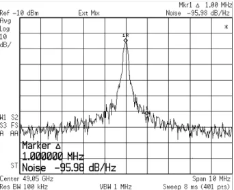
Figure 5. Measured SSB phase noise at 1-MHz offset from 49 GHz. The VCO operates on a 1-V power supply and the quiescent current is 4 mA.
phase noise at 1-MHz offset from 49 GHz is -96 dBc/Hz, as shown in Fig. 5.
The frequency tuning range for a single bias current is 760 MHz as the control voltage varies from 0 V to 1.2 V, and the corresponding VCO gain is 633 MHz/V. Fig. 6 shows the oscillation frequency with respect to the control voltage when the quiescent current is 4mA. The total tunable frequency range is about 1.0 GHz when the bias current varies as well. The variations of the measured signal power and phase noise with respect to the control voltage are shown in Fig. 7. The signal power varies between -25.5 and -26.5 dBm, and the phase noise at 1-MHz offset remains below -94 dBc/Hz. The signal power increases but the oscillation frequency decreases as the quiescent current increases. Fig. 8
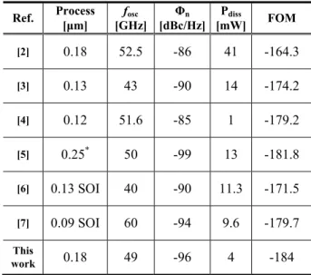
shows the variation of the oscillation frequency and signal power with respect to the quiescent current when the supply voltage is 1V and the control voltage is fixed at 0V. The interaction of signal power, oscillation frequency, and bias current is discussed in detail in [12]. Table I summarizes the performance of this CMOS millimeter-wave VCO.
In order to compare the performance of the VCO with the previously published CMOS VCO fundamentally oscillating above 40 GHz, its measured characteristics is normalized based on the commonly used FOM given by:
Figure 8. Oscillation frequency and corresponding signal power with respect to quiescent current. The supply voltage is 1V and the control voltage is fixed at 0V.
Figure 6. Oscillation frequency with respect to control voltage and VCO bias currents
( ) 20 log 10 log Pdiss
1 mW o n m m f FOM f f = Φ − ⋅ + ⋅ (1)
where fo is the oscillation frequency, fm is the offset
frequency and Pdiss is the power dissipation. The CMOS
VCO of this work achieves a FOM of -184 dBc/Hz, which is the best in comparison with the VCOs implemented in even more advanced COMS or SOI CMOS technology. Table II summarizes the characteristics of the published CMOS VCOs fundamentally oscillating above 40 GHz. The CMOS VCO of this work attains the lowest phase noise of the millimeter-wave VCOs in the standard CMOS technology [2]-[4].
IV. CONCLUSION
A 1-V, 50-GHz fully integrated VCO is implemented in the standard 0.18µm CMOS technology and it achieves a
high
f
oscf
T peak_ ratio of 0.83. The LC-resonant tanks consist of line inductors and NMOS varactors for Q-enhancement. At the power consumption of 4 mW, the measured phase noise at 1-MHz offset from 49 GHz is -96 dBc/Hz, which leads to the best FOM compared with the CMOS VCOs oscillating fundamentally above 40 GHz in even more advanced CMOS technology.ACKNOWLEDGMENT
The authors would like to thank the National Science Council, National Chip Implementation Center, Taiwan, R.O.C., and NTU-MediaTek Wireless Research Laboratory for the support of this work.
REFERENCES
[1] K. Ohata, et al.,“1.25Gbps Wireless Gigabit Ethernet Link at 60 GHz-band,” in IEEE RFIC Symp. Tech. Dig., pp. 509-512, June 2003. [2] C.H. Doan, S. Emami, A.M. Niknejad, R.W. Brodersen, “
Millimeter-wave CMOS design”, IEEE J. Solid-State Circuits, vol.40, pp.144-155, Jan. 2005.
[3] A. P. van der Wel, S. L. J. Gierkink, R. C. Frye, V. Boccuzzi, B. Nauta, “ A robust 43 GHz VCO in standard CMOS for OC-768 SONET applications” European Solid-State Circuits Conference,
Tech. Dig., 16-18 pp.345 – 348, Sept. 2003.
[4] M. Tiebout, H.D. Wohlmuth, W. Simburger, “A 1 V 51GHz fully-integrated VCO in 0.12 µmCMOS,” IEEE ISSCC, Tech. Dig., vol. 1, pp.300-468, Feb. 2002.
[5] HongMo Wang, “A 50 GHz VCO in 0.25 µm CMOS,” IEEE ISSCC,
Tech. Dig, pp. 372 -373, Feb. 2001.
[6] N. Fong, J.-O. Plouchart, N. Zamdmer, Liu Duixian, L. Wagner, P. Garry, G. Tarr, “ A 40 GHz VCO with 9 to 15% tuning range in 0.13 µm SOI CMOS” IEEE VLSI Symp., Digest of Technical
Papers, pp.186 – 189, June 2002.
[7] F. Ellinger, T. Morf, G. Buren, C. Kromer, G. Sialm, L. Rodoni, M. Schmatz, H. Jackel, “60 GHz VCO with wideband tuning range fabricated on VLSI SOI CMOS technology”, IEEE MTT-S IMS,
Dig., vol. 3, pp.1329 - 1332, June 2004.
[8] Ren-Chieh Liu, Hong-Yeh Chang, Chi-Hsueh Wang, Huei Wang, “A 63 GHz VCO using a standard 0.25μm CMOS process,” in
IEEE ISSCC., Tech. Dig., Feb. 2004, pp. 446–447.
[9] Ping-Chen Huang, Ming-Da Tsai, Huei Wang, Chun-Hung Chen, Chih-Sheng Chang, “A 114 GHz VCO in 0.13 μ m CMOS Technology,” in IEEE Int. Solid-State Circuits Conf., Tech. Dig., pp. 404–405 and 606, Feb. 2005.
[10] D. B. Leeson, “ A Simple Model of Feedback Oscillator Noise Spectrum,” in Proc. IEEE, vol. 54, no. 2, pp. 329-330, 1966.
[11] Y.-J. E. Chen, et al., “A low-power Ka-band voltage-controlled oscillator implmented in 200-GHz SiGe HBT technology,” IEEE
Trans. Microwave Theory Tech., vol. 53, pp. 1672-1681, May 2005.
[12] Ye-Ming Li and J. Alvin Connelly, “Modeling A Resonant LC Tank Circuit Enbedded in A VCO,” IEEE ISCAS, Proceedings, vol. 3, pp. 173-176, May 2002.
TABLE I. PERFORMANCE SUMMARY OF THE CMOSVCO
Process 0.18µm CMOS
Supply Voltage 1 V
Power Consumption 4 mW
Phase Noise @ 1-MHz -96 dBc/Hz
Tuning Range 760 MHz / 1 GHz
Core Circuitry Area 90µm
×
120µmTABLE II. RECENTLY PUBLISHED MILLIMETER-WAVE CMOSVCOS
Ref. Process [µm] fosc [GHz] Φn [dBc/Hz] Pdiss [mW] FOM [2] 0.18 52.5 -86 41 -164.3 [3] 0.13 43 -90 14 -174.2 [4] 0.12 51.6 -85 1 -179.2 [5] 0.25* 50 -99 13 -181.8 [6] 0.13 SOI 40 -90 11.3 -171.5 [7] 0.09 SOI 60 -94 9.6 -179.7 This work 0.18 49 -96 4 -184 * modified substrate