國 立 交 通 大 學
材 料 科 學 與 工 程 研 究 所
博 士 論 文
溶液法半導性氧化鋅薄膜製備及其薄膜電
晶體特性研究
The Fabrication and Characteristics of ZnO
Semiconducting Thin Film and Thin Film
Transistors by Solution Method
研 究 生 : 鄭華琦
指導教授 : 陳家富 博士
呂志鵬 博士
溶液法半導性氧化鋅薄膜製備及其薄膜電晶體研究
The Fabrication and Characteristics of ZnO Semiconducting
Thin Film and Thin Film Transistors by Solution Method
研 究 生 : 鄭華琦
Student : Hua-Chi Cheng
指導教授 : 陳家富 博士
呂志鵬 博士
Advisor:Dr. Chia-Fu Chen
Dr. JihPerng Leu
國 立 交 通 大 學
材 料 科 學 與 工 程 學 系
博 士 論 文
A Thesis
Submitted to Department of Material Science and Engineering
College of Engineering, National Chiao Tung University
In partial Fulfillment of the Requirements
for the Degree of Doctor of Philosophy
in Material Science and Engineering
November 2008
Hsinchu, Taiwan, Republic of China
溶液法半導性氧化鋅薄膜製備及其薄膜電晶體研究
學生 : 鄭華琦
指導教授 : 陳家富 博士
呂志鵬 博士
國立交通大學材料科學與工程研究所 博士班
摘要
氧化鋅屬於n 型透明之寬能隙(wide energy band gap, 3.2 eV)半導體,近來廣 泛應用於光電元件及平面顯示器領域。本論文利用溶液法(solution method)成長 氧化鋅(zinc oxide;ZnO)半導性薄膜,並對其薄膜電晶體(thin film transistor;TFT) 之物理及電性做一系列研究;採用的溶液法包含化學浴鍍著法(chemical bath deposition;CBD)與溶膠-凝膠(sol-gel)法。此外利用陽離子調和(cat ion- mediation) 之化學溶液鍍浴方法探討氧化鋅薄膜結晶取向與透光性質,更運用摻雜的原理探
討溶液中鎂離子(magnesium ion;Mg2+)對氧化鋅結晶成長的影響,藉由鎂離子在
溶液中之干擾作用改變氧化鋅結晶之優選方向(prefer orientation),並獲得 90 %良 好透光性氧化鋅薄膜,將能隙(energy band gap)由 3.38 eV 降低至 3.23 eV。最後 利用不同溫度退火的溶膠-凝膠氧化鋅薄膜作為溶液浴鍍著氧化鋅之種子層,研 究溶膠-凝膠結晶種子對溶液浴鍍著氧化鋅之結晶取向的影響,並且以其作為主 動層的全透明薄膜電晶體(transperent thin film transistors;TTFT)元件之電性研究。
在氧化鋅薄膜特性上,主要探討合成之純氧化鋅的結晶性(crystallization)、 光學性質 (optical property)、晶粒大小以及載子濃度(carrier concentration)等物理
性質,以及研究氧化鋅薄膜之形貌,結構,晶相與組成的關係。 在 薄 膜 電 晶 體 應 用 研 究 中 , 探 討 低 溫 成 長 之 氧 化 鋅 薄 膜 在 沒 有 退 火 (annealing)的情況下製作之元件基本電性,其次以溶膠-凝膠法製備不同鎂離子摻 雜之氧化鋅薄膜電晶體,分別探討多元氧化物薄膜與其電晶體之物性與電性,研 究發現氧化鋅藉由鎂的摻雜可以提高膜厚均勻性與透光度,並且使其薄膜電晶體 有較高之電流開關比。 最後利用溶膠-凝膠法與化學溶液浴鍍著法混合成長氧化鋅薄膜,以自體結 晶成核的方式,解決離子摻雜效應對電晶體的影響,並提高載子遷移率,增加元 件開關速度,同時使用铟錫氧化物(ITO)為閘極、源極、和汲極材料,製作全透 明薄膜電晶體元件。針對電性上解決常開效應,並且提高元件開啟時的電流,此 元件為常關型(normally off),或稱增強型(enhancement mode)薄膜電晶體,經元件 結構與薄膜成長方法改善後,可獲得較佳之薄膜電晶體元件(電子遷移率為 0.647 cm2 V-1 s-1;元件之開關比大於 107)。
The Fabrication and Characteristics of ZnO Semiconducting
Thin Film and Thin Film Transistors by Solution Method
Student:Hua-Chi Cheng
Advisor:Dr. Chia-Fu Chen
Dr. Jih-Perng Leu
Institute of Material Science and Engineering
National Chiao Tung University
Abstract
Zinc oxide is an n-type transparent semiconductor with wide band gap of 3.2 eV, which has been extensively applied to photoelectric components and flat panel displays. This thesis was aimed at ZnO thin film preparing by solution method, the properties of the grown ZnO films, and the physical and electrical characteristics of the thin film transistors. The solution methods were including chemical bath deposition (CBD) and sol-gel deposition. In addition, this investigation explored the influence of cation-mediation on the orientation and transmittance of ZnO crystals in chemical bath deposition. Moreover, the doping effect of ZnO crystalline which grown in Mg ion (Mg2+) contained solution was investigated. In particular, the prefer orientation of the ZnO crystalline was changed by the Mg ion mediating in chemical solution. The ZnO crystalline film exhibited good optical transmittance of over 90%. Additionally, the direct band gap value was 3.22eV, which is less than 3.38eV
annealed at different temperatures, which were used as seed layers and nuclei sites for further ZnO films fabrication by chemical bath deposition. Base on the investigation, the influence of sol-gel seed layers on crystallinity and orientation of ZnO by chemical bath deposition were discussed. Also, the electrical characteristics of transparent thin film transistors obtained using this active layer were demonstrated.
In the ZnO films study, the physical properties of the ZnO film by solution methods, including the growth mechanism on crystallization, the optical property, the crystal size, and carrier concentration of the ZnO thin film were investigated. In the ZnO thin film transistors (TFTs) study, the electrical characteristics of ZnO thin film transistors by using low temperature solution process without annealing were demonstrated. In addition, the electrical characteristics of ZnO TFTs with Mg doped and without Mg doped by sol-gel method were demonstrated respectively. The A significant improvement of surface roughness with Mg doping could be noticed. In addition, this result was in good agreement with the discussions of higher current on and current off ratio.
Finally, the ZnO film were grown by sol-gel and chemical solution bath combination method, to resolve the doping effect on thin film transistors by using the self-crystal as the growing sites for further deposition. Since indium tin oxide was used as the conducting electrodes (source, drain, and gate) for transparent thin film transistors. Current-voltage properties measured through the gate infer that the ZnO channel was n-type enhancement mode device due to a positive gate voltage were required to induce a conducting channel, and the current increases with increasing positive gate bias. The optimum device had field-effect mobility of 0.67 cm2 /V s and an on-off ratio more than 107.
誌 謝
感謝國立交通大學所有教導過我的老師,尤其是我的指導教授-陳家富老 師。工作多年後,再度接受更高的學術訓練,陳老師當初授予我跨領域學習的機 會,謝謝他在研究上的指導與鼓勵,更重要的是對學生的照顧愛護與觀念上的導 正。 感謝學弟妹在實驗上提供意見及討論以及庶務上事務的幫忙。以及曾在工作 上的好同事目前任職於逢甲大學的蔡健益博士,不僅提供不少的建議及指教,並 在研究上給予協助。謝謝工研院與TTLA 的長官及同仁的支援;此外,感謝任職 於台積電的好朋友們加油鼓勵,得以使研究遇到瓶頸時獲得突破。 感謝我的家人,這些年來的精神支持,讓我能同時兼顧家庭、工作、與學業, 完成取得博士學位的心願。 最後,僅以此論文獻給在天上最敬愛的父親,雖然這項喜悅來不及讓您親身 感受,但是,我做到了! 數年來,有著無數人的幫助,要謝的人太多了,一切恩惠銘記在心。Contents
Page
Abstract (Chinese)
--- I
Abstract (English)
--- III
Acknowledge (Chinese) --- V
Contents --- VI
List of Figures
--- X
List of Tables
--- XIII
Chapter 1 Introduction ---
1
1.1 Background --- 1
1.2 Motivations --- 2
1.3 Organization of this Thesis --- 4
Chapter 2 A brief literature review and technical background ---
6
2.1 Application of Thin Film Transistor on Liquid Crystal Display (TFT-LCD) ---
6
2.2 Overview of thin film transistor --- 10
2.3 Transparent metal oxide semiconductors --- 14
2.4 Zinc oxide ---
15
2.5 Device structure of Thin Film Transistor --- 19
2.6 Basic operation of TFT device --- 20
Chapter 3 Experimental method and measurement techniques ---
23
3.1 Experimental Details --- 23
3.1.1 The sol-gel method ---
23
3.1.2 Synthesis of the precursors --- 24
3.1.4 The fabrication of thin film transistor devices --- 26
3.2 Characterization for materials and devices --- 26
3.2.1 Scanning electron microscopy (SEM) --- 26
3.2.2 Transmission electron microscopy (TEM) --- 26
3.2.3 X-ray diffraction spectroscopy --- 27
3.2.4 UV absorption --- 27
3.2.5 Thermal gravimetric analysis ---
27
3.2.6 Hall effect measurement --- 28
3.2.7 Atomic force microscope (AFM) ---
30
3.2.8 X-ray photoelectron spectroscopy --- 31
3.3 Electrical properties measurement for TFT devices --- 31
Chapter 4 Results and Discussions ---
32
4.1 Thin film transistors with active layers of zinc oxide (ZnO) fabricated by low-temperature chemical bath method
--- 32
4.1.1 Descriptions ---
32
4.1.2 Conceptions --- 32
4.1.3 Specifics methods --- 33
4.1.3.1 Film deposition procedure ---
33
4.1.3.2 Characterization techniques --- 35
4.1.4 Achievements and explanations --- 35
4.1.5 Summary ---
39
4.2 Cation-Mediated Effects on Zinc Oxide Films Formed by Chemical Bath Deposition
--- 40
4.2.1 Descriptions ---
40
4.2.3.1 Deposition of films ---
41
4.2.3.2 Characterization ---
42
4.2.4 Achievements and explanations --- 42
4.2.5 Summary ---
49
4.3 Performance of sol-gel deposited Zn1-xMgxO films used as active channel layer for thin-film transistors
--- 50
4.3.1 Descriptions ---
50
4.3.2 Conceptions --- 50
4.3.3 Specifics methods --- 52
4.3.4 Achievements and explanations
--- 53
4.3.5 Summary ---
61
4.4 High-quality oriented ZnO films by sol-gel and chemical bath deposition combination method
--- 62
4.4.1 Descriptions ---
62
4.4.2 Conceptions --- 62
4.4.3 Specifics methods --- 63
4.4.4 Achievements and explanations --- 64
4.4.5 Summary ---
71
4.5 Transparent ZnO thin-film transistor fabricated by sol-gel and chemical bath deposition combination method
--- 72
4.5.1 Descriptions ---
72
4.5.2 Conceptions --- 72
4.5.3 Specifics methods --- 73
4.5.4 Achievements and explanations --- 75
4.5.5 Summary ---
79
5.1 Conclusions --- 80
5.2 Suggestions --- 81
Reference --- 83
List of Figures
Fig. 2.1 (a) the cross-sectional view of the whole panel, and (b) the storage capacitor-on-gate of one sub-pixel design ---
9
Fig. 2.2 Schematic cross-sectional views of TFTs: (a) adapted from Lilienfeld [32]at U.S. Patent 1930; (b) Weimer [33] at 1962 IRE; and (c) Spear and LeComber [37] at 1979 IEEE ---
10
Fig. 2.3 The hexagonal (wurtzite) crystal structure of ZnO ---16
Fig. 2.4 Four basic TFT structures: (a) co-planar top gate, (b) co-planar bottomgate, (c) staggered top gate, and (d) staggered bottom gate ---
19
Fig. 2.5 (a) The basic structure of a TFT and the corresponding energy banddiagrams as viewed through the gate for several conditions, including (b) equilibrium, (c) VGS < 0 and (d) VGS > 0 ---
21
Fig. 3.1 The flow chart of the precursor preparation and ZnO films processing byspin coating ---
25
Fig. 3.2 Schematic of the Hall effect in a long, thin bar of semiconductor with fourohm contacts. The direction of the magnetic field B is along the z-axis and the sample has a finite thickness d ---
29
Fig. 4.1 Schematic (a) cross-sectional and (b) top view of the ZnO-based thin-filmtransistor ---
34
Fig. 4.2 X-ray diffraction spectrum of the ZnO thin film on SiO2 surface preparedby the CBD ---
36
Fig. 4.3 SEM images of ZnO film deposited at 60℃ from 0.1 mol/L zinc nitrateand 0.03 mol/L ---
37
Fig. 4.4 Electrical characteristics of the ZnO-TFT which the active channel layerZnO was fabricated by CBD method (a) Id-Vd curve, (b) Id-Vg curve ---
38
Fig. 4.5 XRD pattern of ZnO films: (a) growth without cation mediation in thesolution bath and (b) growth with cation mediation in the solution bath ---
43
Fig. 4.6
SEM images of ZnO film: (a) cross-sectional morphology and (c) plane-view morphology of film deposited in bath without cation mediation solution; (b) cross-sectional morphology, and (d) plane-view morphology of film deposited in cation-mediated-solution bath
Fig. 4.7 EDS of ZnO film deposited in cation-mediated solution bath ---
45
Fig. 4.8 Lattice constants of ZnO in both a and c-axes ---46
Fig. 4.9 Optical transmittance spectra of ZnO films deposited in (a) bath withoutcation-mediated solution and (b) cation-mediated-solution bath ---
47
Fig. 4.10 Square of the absorption coefficient as a function of photon energy forZnO growth in (a) bath without cation-mediated solution and (b) cation-mediated- solution bath ---
49
Fig. 4.11 TGA-DSC curves of the dried of Zn1-xMgxO sols with x=0, 0.2 or 0.3 ---54
Fig. 4.12 X-ray diffraction patterns of Zn1-xMgxO thin films (0≦x≦0.36) , whichwere annealed at 500 oC for 1 hr ---
55
Fig. 4.13 SEM micrographs of cross-sections of Zn1-xMgxO thin films: (a) x=0; (b)x =0.2; (c) x=0.3 and (d) x=0.36 ---
56
Fig. 4.14 SPM images of the surface of Zn1-xMgxO thin films: (a) x =0; (b) x= .2;(c) x=0.3 and (d) x=0.3 ---
58
Fig. 4.15 The transmittance spectra of Zn1-xMgxO thin films with x=0, 0.2, 0.3 or0.36 ---
59
Fig. 4.16 (a) Output characteristics (ID-VD curve) and (b) transfer characteristics(ID-VG curve) of TFT using Zn0.8Mg0.2O thin film as the active channel layer ---
60
Fig. 4.17 Typical TGA/DSC curves measured in air at a heating rate of 5℃/min forZnO sol-gel ---
65
Fig. 4.18 X-ray diffraction pattern of ZnO films, seed layers post-baked at (a)150℃, (b) 250℃, and (c) 550℃; combination ZnO films of CBD ZnO films grown on post-baked seed layers at (d) 150℃, (e) 250℃, and (f) 550℃ ---
66
Fig. 4.19 (a) TEM image and the (b) SEAD patterns of the ZnO film on glasssubstrate ---
67
Fig. 4.20 SEM images of ZnO film; seed layers post-baked at (a) 150℃, (b) 250℃,and (c) 550℃; combination ZnO films of CBD ZnO films grown on post-baked seed layers at (d) 150℃, (e) 250℃, and (f) 550℃ ---
68
Fig. 4.21 XPS pattern of ZnO films which the CBD ZnO film grown on post-bakedFig. 4.22 The Hall-effect mobility of the ZnO films grow by sol-gel and CBD combination method ---
70
Fig. 4.23 Top-gate structure of ZnO- TFT in which (a) is cross-sectional schematicand (b) is top view schematic ---
74
Fig. 4.24 SEM images of (a) ZnO films on Corning 1737 glass substrate by 45° tiltangle, the insert is a cross section view of scale up from the local of ZnO film with a 400 nm scale. (b) local cross section view of ZnO-TFT on Corning 1737 glass substrate ---
76
Fig. 4.25 Optical transmission spectra for the Top-gate structure of ZnO-TFT(except substrate) through the ITO film (gate), SiNx (gate insulator), and (ZnO film) channel region, and the thicknesses are 100nm, 300nm, and 200nm respectively. The insert shows a 5 × 5 cm2 substrate with 75 devices of ZnO-TFT on Corning 1737 glass substrate ---
77
Fig. 4.26 (a) Drain current-drain voltage (ID-VD ) curves at gate voltage (VG )between 0 and 40V for a ZnO-TFT with channel width to length ratio (W/L) of 50. (b) Transfer characteristics, ID versus VG at VDS =20V for the same ZnO-TFT. It is also indicated the square root of drain current versus the gate voltage from which is determined the threshold voltage ---
79
List of Tables
Table 2.1 TFT/AMLCD Design Factor ---
8
Table 2.2 Processing methods employed and electrical performance characteristicsfor several fully transparent ZnO TFTs. ---
13
Table 2.3 Thin film electrical and optical properties of n-type transparentconductors ---
15
Table 2.4 Physical properties of wurtzite ZnO ---18
Table 4.1 Chemical composition of the solutions used for ZnO film deposition ---42
Chapter 1
Introduction
2/2 Background!
Recently, researchers have paid increasing attention to new materials for accomplishing specific demands. In the electronic applications, good transparency, high performance, simple fabrication, low cost, and no environmental concerns are nowadays a crucial requirement in materials for the next generation application. The only possibility to perform transparent device is by using oxide materials. These oxide materials are very interesting materials because they combine simultaneously high/low conductivity with high visual transparency and have been widely used in a variety of applications.!
In the past, devices based on Si base had presented some limitations, such as light sensitivity, light degradation, and must be processed in expensive equipments. Therefore, investigate on the new material developing is necessary and important.
Oxide-based materials, a branch of material research, supplying a great platform for applications in optical electronic field, represents rapidly expanding research area due to their potential applications in electronics [1], optoelectronics [2], catalysts [3], sensors [4] and so on. Recently, the ZnO-based material was paid much attention, since it was multifunction and used in additives, medicines and optical devices[5-9]. Moreover, crystalline ZnO-based thin films have attracted considerable interest as a transparent conductive oxide and as a semiconductor in both the visible spectrum and part of the UV range. Crystalline ZnO materials exhibit electro-optical properties, high electro-chemical stability, large band gap, abundance in nature and absence of
toxicity which make them very popular for use in solar cells[10], photo detectors[11], light-emitting devices[12], gas sensor elements[13] and surface acoustic wave guides [14], which could lead to improving progress in solid state devices development.
Crystalline ZnO, in particular, provide a growing number of applications which apparently depend on its growth constitution. In practical applications, the shape, size and arrangement of crystallites limit suitability of films to specific functions. Therefore, microstructure and crystallinity should be improved further, and both simple and low cost methods for preparing high-quality ZnO should be studied. Based on the backdrop the above, it is possible to accelerate the progress of materials development in advance electronic elements.
Many methods for ZnO preparing, including chemical and physical, such as sputtering[15], pulsed laser deposition[16], chemical vapor deposition (CVD)[17], molecular beam epitaxy[18] and sol-gel process[19]. Several methods for growing ZnO films at low temperature that use solution methods have been reported[20-25]. Among these, solution method is of particular interest because of its simplicity, low cost and the large area of its coatings. However, the solution method is based on the controlled precipitation of the material to be prepared, so as to form a film upon the substrate surface. Also, the morphologies depend on the control of precipitation during film growth. Numerous articles have addressed control of the growth mechanism to adjust the formation of the crystal [26-28]. More stable and consistency microstructures must be improved for further applications.
1.2 Motivations
and wide band gap. ZnO-based TFTs exhibit higher transparency in visible wavelength and relative low process temperature compare with the silicon-based TFTs, thus has received much attention recently. Several methods are applied to prepare ZnO films, both physical and chemical deposition technologies, which include magnetron sputtering [29-43], pulsed laser deposition [44-48], chemical vapor deposition (CVD) [18], molecular beam epitaxy [19], and sol-gel process [49] etc.. The mobility of devices demonstrates among the researches ranging from 0.05 to 70 cm2/Vs by those methods. However, most of the methods were not well suited for large area coating and low temperature processing; especially for those need vacuum facilities which result in high cost. For the issues, beside the deposition methods of ZnO films involving vacuum facilities mentioned, some studies [17, 50, 51] investigated another deposition method, chemical solution deposition (CSD), a method for films growth in atmosphere. For large area deposition, the CSD process may provide a more economic way to fabricate device components than vacuum techniques. Moreover, from the scientific point of view, polycrystalline ZnO based films are generally recognized in electronic application that high quality crystalline materials can be applied to semiconductor in active devices. It will stir a new field of research on the ZnO thin films deposition by solution method. Also, it will provide a new simple and direct patterning which approach to deliver high performance n-type ZnO TFTs.
From the industrial point of view, low temperature, simple, and low cost method are regarded as excellent technique for TFTs fabrication. Currently, increasing the aperture ratio of the TFT-LCD is only of the main topic that are able to save the power consumption resulted from poor backlight transmission through low aperture ratio
pixel structure. In addition, the excellent device characteristics of ZnO based TFTs can be fabricated directly on the glass substrates of displays, which makes the integration of LCD pixel with complicated driving circuits possible.
We believe these approaches of generating high-quality ZnO based TFTs will not only stir the fundamental research on new electronic application and characterizations on the polycrystalline semiconductor but also benefit the new industry in Taiwan to develop low-cost, highly reliable, transparent and flexible electronics.
However, most of the methods are not well suited for large area coating and low temperature processing. For the issues, chemical bath deposition (CBD) has been an attractive technology which is simple and low-cost for fabricating thin film. There are many previous articles discussing the ZnO films using electroless deposition in solution bath and indicating the feasibility of low temperature [15-19]. These make the films good compatibility with substrate materials.
1.3 Organization of this Thesis
There are other four chapters in this thesis. A concise summary of these chapters is described as follows:
Chapter 2 A brief literature review and technical background: The aim of this
chapter is to provide a basic understanding about ZnO and its thin film transistors application concept. A general overview of transparent conducting oxide semiconductors, followed by a detailed exploration of zinc oxide properties is presented. In addition, basic TFT operation, TFT structures, and ZnO-based TFTs are reviewed.
solution methods for ZnO films depositing are introduced. Also, thin-film processing techniques relevant to the fabrication of TFTs are briefly discussed. Finally, thin-film characterization techniques are discussed, including crystallinity, morphology, Hall and optical transmission measurements etc..
Chapter 4 Results and Discussions: There are five subjects in this chapter. Research
objectives listed above are interpreted, and the more concerned literature review is also discussed in this chapter.
Chapter 5 Conclusions and Suggestions: The results of the present investigation are
summarized. On the other hand, some proposed relevant works are provided for further study.
Chapter 2
A brief literature review and technical background
2.1 Application of Thin Film Transistor on Liquid Crystal Display (TFT-LCD)
The technologies and applications of AMLCDs are developing rapidly in recent decades. The products such as portable computer, projection light valve, and miniature display, owing to their characteristics including the brightness, viewing angle, low power consumption, and integrated circuit (IC) process compatibility. In the past, the cathode ray tubes (CRTs) played the leading role in display electronics. However, CRTs have been completely replaced by LCDs. AMLCDs have penetrated into the desktop monitor market and even take possession of the market of television. Desktop monitor engineering specifications emphasize high visual performance, such as higher resolution, higher pixel content, wider viewing angle, larger color gamut, higher brightness and a moderate price. Another large area display product, such as HDTV (high definition television), would underscore lower cost while accepting a lower cost while accepting a lower cost while accepting a lower resolution and lower pixel content display. However, in order to quickly occupy the TV market, several AMLCD makers increase the size of LCD panels rapidly.
Even the fabrication cost of passive-matrix is slightly lower than that of active-matrix arrays, it would be important to understand why an active matrix array design is necessary. A TFT is a MOSFET fabricated on an insulating substrate (preferably glass for low cost products) by employing all thin film components. It has all the advantages of a silicon-on-insulator (SOI) device; fabrication simplicity, strong latch-up, immunity and possible high packing density. When TFTs are used in
AMLCDs, the semiconductor film of TFT channel is composed of either amorphous Si (a-Si), various degrees of recrystalized a-Si (poly-Si), or II-VI group semiconductors such as CdSe and ZnO, and most recently, even organic materials, such as pentacene, are being considered. The computer simulations are commonly used to optimize the TFT active-matrix array design and analyze the electrical performance of the TFTs based on statistical extraction of the devices and fabrication process parameters. Since this approach is the most efficient way to predict the statistical mean and variance in display performance, it is more instructive to carry out a simple, physically based parameter analysis to identify functional dependencies, performance limits, and minimum requirements, and this analysis is applicable to any kind of TFT processing technologies. Table 2.1 [52-54] list the major TFT and AMLCDs design factors. The pixel size, the TFT geometry, and the desired fill factor will determine the amount of parasitic capacitance to the adjacent rows and columns, while the display size and pixel content will dictate the resistance of the row and column lines. The number of rows and the frame time dominate the charging time of the pixel capacitance, including the liquid crystal capacitance and charge retention time. The minimum TFT on-state current determines the number of gray levels to accurately charge up the pixel. The LC mode will dictate the pixel voltage, and the allowable gray bit error rate, along with specifications for flicker, will determine the TFT and pixel off-state current.
Table 2.1 TFT/AMLCD Design Factors and Examples
TFT AMLCD design factors Examples
Display size Diagonal (14”, 15”, 18”, 20”, 40”, etc.)
Light modulator/ mode (TNLC-NW, TNLC-NB, IPS, FELC, etc.
Illumination conditions Contrast ratio (2:1, 300:1, etc.)
Maximum brightness (100 cd/m2, 500 cd/m2, etc.)
Ambient illumination (dark room, room light, sunlight readable, etc.)
Display format (number of lines) Content (VGA, SVGA, XGA, SXGA, UXGA, QUXGA-W, etc.)
Frame time Film, 1/24 sec; video, 1/30 sec; data 1/60 sec etc.
Number of gray levels 6-bits (262K colors), 8-bits (16.8M colors), etc.
TFT geometry Bottom-gate staged BCE, I-stopper, top gate, etc.
(a)
(b)
Fig. 2.1 (a) the cross-sectional view of the whole panel, and (b) the storage capacitor-on-gate of one sub-pixel design.
TFTs have been intensively researched for possible electronic and display applications. In the early 1960’s TFT technology was in competition with single
crystal silicon MOSFET for the integrated circuit field. Due to the rapid progress of the latter and the difficulty in consistently producing good quality devices of the former, TFTs were not successful at that time. However, the application of TFTs to displays will not be given up. The first active matrix LCD (AMLCD) was realized in 1973. Fig. 2.1 shows (a) the cross-sectional view of the whole panel, and (b) the storage capacitor-on-gate of one sub-pixel design.
Fig. 2.2 Schematic cross-sectional views of TFTs: (a) adapted from Lilienfeld [55] at U.S. Patent 1930; (b) Weimer [56] at 1962 IRE; and (c) Spear and LeComber [57] at 1979 IEEE.
as 1925 and patented in 1930 [55] (see Fig. 2.2(a) where an adaptation of the cross section of the device is shown), the first TFT was demonstrated by P. K. Weimer of RCA Laboratory in 1961 [58]. The represented device is now called a staggered structure, which was composed of polycrystalline cadmium sulfide, similar to those developed for photo detectors, and monoxide as insulator films. The simplified structure is shown in Fig. 2.2(b).
In LCD application, the first CdSe TFT was used as a switching element by Brody et al. in 1973 [59]. Even though the many successful demonstrations of TFT LCDs, the industry did not enter in this market until the report on the feasibility of doping amorphous silicon (a-Si:H) by the glow discharge technique [57, 60]. LeComber, Spear and Ghaith reported the first a-Si:H TFT in 1979s [61], whose structure is indicated in Fig. 2.2 (c). The hydrogenated amorphous silicon could be doped with donors or acceptors to reduce n- or p-type conductivity, in contrast to pure amorphous silicon in previous investigation [62]. Furthermore, LeComber et al. demonstrated TFT which fitted criteria for driving liquid crystal display, as published by Brody [59]. The first polycrystalline silicon grown by chemical vapor deposition was employed to achieve good electrical properties, which was proposed by Depp et al. [63] in 1980s. In order to achieve good electrical performance, chemical vapor deposition was used for the polycrystalline silicon growth, the gate insulator SiO2 grown at 10503 thermally, quartz was utilized as substrates for the poly-Si TFTs.
IBM [64] and Mitsubishi [65] groups used laser recrystalization approach to improve the mobility and threshold voltage of poly-Si TFTs by 1982, and an electron mobility of 400 cm2/Vs was obtained. The purpose of mobility improving was ot integrate the driving circuits matched with providing pixel TFTs. In general, the a-Si
TFT technology is more popular, which could be used for commercial products such as AMLCDs in portable computers application. However, for high speed response application, poly-Si TFTs are superior to a-Si TFTs in mobility performance. For the reason, the pixel transistors and high speed circuits must be operated in coordination. Recently, TFTs have undergone extensive evolution, development, and refinement. The potential for new applications, lightweight, mechanically robust electronics for displays and other devices on flexible substrates have motivated considerable research on new materials [65–68] and improved processes [69,70] for fabricating thin film transistors. More recently, transparent electronics are nowadays a crucial technology of optoelectronic devices. Oxide semiconductors are very interesting materials because they combine simultaneously high/low conductivity with high visual transparency and have been widely used in a variety of applications (e.g. antistatic coatings, touch display panels, solar cells, flat panel displays, heaters, defrosters, optical coatings, among others) for more than a half-century. A new generation of oxide semiconductors are being studied and applied as the active material to TFT, in special zinc oxide (ZnO). Transparent oxide based semiconductor transistors have been proposed using as active channel non-doped ZnO, because of its low photosensitivity, no environmental concerns, and especially high mobility [50, 51, 71–76].
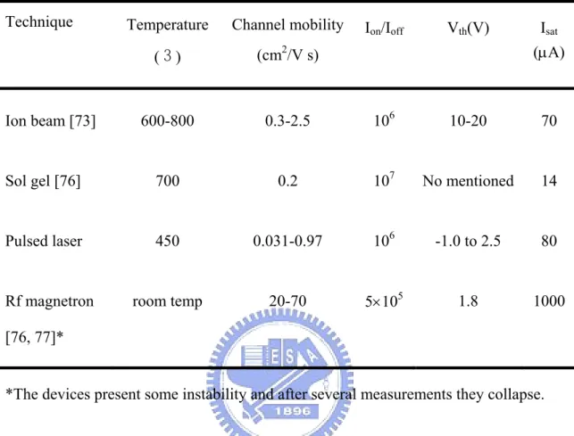
Table 2.2 summarizes the processing methods employed in fabrication of several transparent channel-layer TFTs and their electrical performance characteristics. All the channel mobility, current ratio, and threshold voltage can be compatible to amorphous Si TFTs.
Table 2.2 Processing methods employed and electrical performance characteristics for several fully transparent ZnO TFTs.
Technique Temperature (3) Channel mobility (cm2/V s) Ion/Ioff Vth(V) Isat (μA) Ion beam [73] 600-800 0.3-2.5 106 10-20 70
Sol gel [76] 700 0.2 107 No mentioned 14
Pulsed laser 450 0.031-0.97 106 -1.0 to 2.5 80
Rf magnetron [76, 77]*
room temp 20-70 5×10⁵ 1.8 1000
*The devices present some instability and after several measurements they collapse.
One of the main advantages exhibited by these transistors rests on the influence of the electron channel mobility which leading to higher drive current and faster device operating speed. Oxide-based transistors have recently been proposed as active channel [29, 30, 51, 71-77]. Among them, wurtzite structured ZnO thin films have been studied as the active layer in the TFTs! because of its low cost, low photosensitivity, no environmental concerns, and especially high mobility. In fact, ZnO has the greatest potential to grow high quality crystalline zinc oxide at low temperature. This is particularly advantageous for electronic drivers, which need to be processed at temperature that is low enough to be compatible with plastic substrates. Nowadays, TFTs based on α-Si:H have presented some limitations, such as light
sensitivity, light degradation, and low mobility. On the contrary, TFTs based on ZnO are transparent in the visible region of the spectra and less light sensitive. Besides, because of their high transparency, high mobility, simple processing method, and low cost, ZnO is presently attracting much attention due to its possibilities for replacing amorphous Si that has been widely used as the channel layer in conventional TFTs [71-73].
2.3 Transparent metal oxide semiconductors
Transparent property is nowadays a new target for materials development in electronics application. The simultaneous existence of optical transparency and electrical conductivity require a wide band gap (≥3 eV) material which due to the large electro negativity of oxygen [84], doping is a general method for modulate the Fermi level close enough to the conduction (valence) band to induce mobile electrons (holes). For the relatively low mobility exhibited by this class of materials, typical transparent conductors used in passive applications are degenerately doped in order to maximize their conductivity.
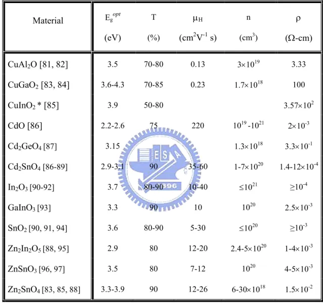
Transparency oxide semiconductors are currently utilized in a number of applications, including thin-film solar cells and flat-panel displays. The first report of p-type conductivity in a transparent material (CuAlO2) came in 1997 [81]. After that, a number of new p-type as well as n-type transparent conducting materials have been discovered.Table 2.3 lists known n-type semiconductors along with typical values of important thin film electrical and optical properties (optical bandgap, average transmission in the visible region, Hall mobility, carrier concentration, and conductivity) as available. In Table 2.3, Egopt
typical optical transmission in the visible region, μH denotes typical Hall mobility, n denotes typical carrier concentration, and ρ denotes typical resistivity.
Table 2.3 Thin film electrical and optical properties of n-type transparent conductors. Material Egopt (eV) T (%) μH (cm2V-1 s) n (cm3) ρ (Ω-cm) CuAl2O [81, 82] 3.5 70-80 0.13 3×10¹⁹ 3.33 CuGaO2 [83, 84] 3.6-4.3 70-85 0.23 1.7×10¹⁸ 100 CuInO2 * [85] 3.9 50-80 3.57×10² CdO [86] 2.2-2.6 75 220 1019 -1021 2×10⁻³ Cd2GeO4 [87] 3.15 1.3×10¹⁸ 3.3×10⁻¹ Cd2SnO4 [86-89] 2.9-3.1 90 35-60 1-7×10²⁰ 1.4-12×10-4 In2O3 [90-92] 3.7 80-90 10-40 ≤1021 ≥10-4 GaInO3 [93] 3.3 90 10 1020 2.5×10⁻³ SnO2 [90, 91, 94] 3.6 80-90 5-30 ≤1020 ≥10-3 Zn2In2O5 [88, 95] 2.9 80 12-20 2.4-5×10²⁰ 1-4×10⁻³ ZnSnO3 [96, 97] 3.5 80 7-12 1020 4-5×10⁻³ Zn2SnO4 [83, 85, 88] 3.3-3.9 90 12-26 6-30×1018 1.5×10⁻² *Bipolar conductive material [81, 94]
2.4 Zinc oxide
Zinc oxide, known as zincite in mineralogy, was first described in North America around 1810 as the red oxide of ZnO is one of zinc. It is silvery-gray colour in pure form. Zinc oxide can take the form of two different crystallographic structures namely
the zinc-blend structure and wurtzite structure (show as Fig. 2.3). The zinc-blend structure is composed of two interpenetrating face-centered cubic (fcc) sub-lattices, while the wurtzite structure consists of two interpenetrating hexagonal close packed (hcp) sub-lattices, which have the similar properties to GaN [100].
Fig. 2.3 The hexagonal (wurtzite) crystal structure of ZnO
ZnO is one of the group Ⅱ-Ⅵ materials, in the new century, gradually becomes the new focus in material research because it has a wide direct band gap (Eg= 3.3eV, while Eg= 3.4eV for GaN [100]) at room temperature (RT), a high exciton binding
energy (Eb=60meV, while Eb=28meV for GaN [101]) and a direct transition character, band states arising from point defects, interstitial zinc ions, oxygen vacancies or dislocations, which allow its use in a number of applications. It is one of the common transparent conducting materials [102]. Also, ZnO can function as a phosphor (cathodoluminescent [103], photoluminescent [104, 105], electroluminescent [106]); as a thin film chemical sensor [107]; and as a piezoelectric material [108]. The band gap energy of ZnO could be changed via substituting various cation ions into the lattice. For the electrical properties of ZnO-based device, controlling over the carrier concentration of ZnO is important. The carrier concentration of ZnO was not only affected by the intrinsic crystal defects (the interstitial zinc ions and oxygen vacancies) but also influenced by the extrinsic impurities, called dopants. The intrinsic defects and dopants determine the domination of the ZnO were electrons or holes. The basic physical properties of ZnO are summarized in Table 2.4 [109]. Since ZnO has melting temperature as high as 2248K. The strength of Zn-to-O bond is larger than that of Ga-to-N. Moreover, ZnO could resistive to high energy radiation [110-112], which is suitable for application in air. These excellent properties of ZnO make a good candidate material for optical devices, such as blue LED’s, and semiconductor devices besides widely used GaN [113].
ZnO thin films have been deposited using a number of methods, including reactive sputtering (DC [114], RF [114], and ion beam [115]), activated reactive evaporation (ARE) [116], spray pyrolysis [117], sol-gel [118], laser ablation [119], pyrosol [77], metal-organic chemical vapor deposition (MOCVD) [74], and electrochemical reaction [75]. Among these, solution route is of particular interest because of its simplicity, low cost and the large area of its coatings.
Table 2.4 Physical properties of wurtzite ZnO.
Property Value
Lattice parameters at 300K:
a0 0.32495nm
c0 0.52069
a0 / c0 1.602(1.633 for ideal hexagonal
structure)
u 0.345
Density 5.606 g/cm3
Stable phase at 300K Wurtzite
Melting point 19753
Thermal conductivity 0.6, 1-1.2
Linear expansion coefficient (/3) a0: 6.5×10⁻⁶ , c0: 6.5×10⁻⁶
Static dielectric constant 8.656
Refractive index 2.008, 2.029
Energy gap 3.4eV(direct band gap)
Intrinsic carrier concentration < 106 cm-3
Exciton binding energy 60meV
Electron effective mass 0.24
Electron Hall mobility at 300K for low n-type conductivity
200 cm2/Vs
Hole effective mass 0.59
Hole Hall mobility at 300K for low p-type conductivity
2.5 Device structure of Thin Film Transistor
The four basic TFT structures are showed in Fig. 2.4, which have co-planar top-gate, co-planar bottom gate, staggered top-gate, and staggered bottom-gate [123]. Electrodes placement distinguished the various structures, i.e. electrodes are placed on opposite sides of the interface (and hence the channel) for staggered structures, while electrodes are placed on the same side of the interface for the co-planar structure.
Fig. 2.4 Four basic TFT structures: (a) co-planar top gate, (b) co-planar bottom gate, (c) staggered top gate, and (d) staggered bottom gate.
Process integration is determined on the use of different structures. In the coplanar top-gate structure, the semiconductor is deposited first. Therefore, the maximum semiconductor processing temperature is limited only by the semiconductor and the substrate. The co-planar structure is difficult to realize in some technologies, damage from implantation cannot be remedied. This implies that the channel must be protected during implantation.
For both bottom-gate structures, the insulator is deposited first. The channel (a) (b)
(c) (d)
S
Suubbssttrraattee
Source & Drain Semiconductor
Insulator
layers would not be damaged by plasma-induced, such as RF sputtering or plasma-enhanced chemical vapor deposition (since insulator deposition typically requires the use of a higher power as compared to deposition of other layers).
2.6 Basic operation of TFT device
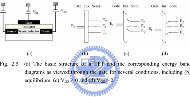
For the general principles just discussed, a TFT, the structure and energy band diagrams as showed in Fig. 2.5 Talking the semiconductor to be n-type, consider first the application of a positive bias. The equilibrium band diagram shown in Fig. 2.5(b) assumes an ideal situation, i.e. there is no charge in the semiconductor before the application of a gate bias.
Consider several biasing schemes showed in Fig. 2.3, VGS < 0, 0 ≤ VGS ≤ Vth , and VGS =Vth , where VGS is the gate-source voltage and Vth is the threshold voltage. For the application of a small negative sloping of the energy bands in both the insulator and semiconductor, as displayed in Fig. 2.5(b). It is clear that the concentration of majority carrier electrons has been decreased and depleted, in the vicinity of the insulator-semiconductor interface. A similar conclusion results from charge considerations. Setting VGS < 0 places a minus charge on the gate, which in turn repels electrons from the insulator-semiconductor interface and exposes the positively charged donor sites. This particular situation, where the electron concentrations at the insulator- semiconductor interface are less than the background doping concentration, is known for obvious reasons as depletion.On the other hand, application of a small positive gate bias (0 ≤ VGS ·≤ Vth ) attracts electrons towards the interface, creating an accumulation layer (or channel) near the interface and a depletion region in the bulk. Biasing in this “subthreshold” regime causes downward
band bending in the insulator and the semiconductor (near the interface), as shown in Fig. 2.3(d). Increasing the gate bias modulates the conductivity of the surface layer and is reflected in an increased degree of band bending. The gate voltage at which there is an appreciable electron carrier density present at the interface establishes the threshold voltage (i.e. VGS = Vth).
(a) (b) (c) (d)
Fig. 2.5 (a) The basic structure of a TFT and the corresponding energy band diagrams as viewed through the gate for several conditions, including (b) equilibrium, (c) VGS < 0 and (d) VGS > 0.
The application of VGS > 0 lower EF in the gate relative to EF in the semiconductor and causes a positive sloping of the energy bands in both the insulator and semiconductor. As show in the result energy band diagram, Fig. 2.3(d), the major conclusion to be driven is that the electron concentration inside the semiconductor increases as one approached the insulator-semiconductor interface. This particular situation, where the majority carrier concentration is greater near the insulator- semiconductor interface than in the bulb of the semiconductor, is known as accumulation.
Now that channel formation has been established, application of a positive voltage on the drain attracts electrons towards the drain and accounts for the drain
current, ID. Initially, the channel is modeled as a resistor, i.e. linearly increasing drain current with drain-source voltage, VDS. Continuing to increase the drain voltage obviously causes the channel to narrow more and more, especially near the drain, until eventually the top and bottom depletion regions touch in the near vicinity of the drain. The complete depletion of the channel, touching of the top and bottom depletion regions, is an important special condition and is referred to as “pinch-off”. When the channel pinches off inside the device, the slop of the ID-VD characteristic becomes approximately zero, negating the effect of the surface accumulation layer, and the drain bias at the pinch-off point is given the designation VDsat. For drain biases in excess of VDsat, the ID-VD characteristic saturates, that is, remains approximately constant at the IDsat value.
Chapter 3
Experiments and measurement techniques
3.1 Experimental methods 3.1.1 The sol-gel method
Sol-Gel method is one of the promising processes to prepared high quality thin films at relative low temperatures compared to other depositions. The first step to form the gels in the sol-gel process is hydrolysis, a hydroxyl attached to the metal atoms as in the following reaction [124]:
M(OR)n + H2O →M(OR)n-1(OH) + ROH (3-1) The R and ROH represented a ligand and an alcohol. The second step of sol-gel process is polymerization which was achieved by two partially hydrolyzed molecules linked together, such as
M(OR)n + M(OR)n-1(OH) → M2O(OR)2n-2 + H2O (3-2) A long chain molecule could be obtained from the reaction of hydrolysis and polymerization mentioned above. Since the coating ability and preferential direction of thin preparation of thin films depend on the molecules, the reaction plays an important role in the preparation of thin films. In an organic system, the solute is usually the metal alkoxide, such as M(OR)n which M is represented metal and R represented alkyl group(CH3, C2H5,…..etc.).
As a result of the sol-gel solution still maintains liquid phase before gelled, and is easy to film on different substrates. There are many coating methods, such as dip
coating, spray coating, and spin coating. The quality of the thin films depends on coating method and coating conditions.
Among the wet coating approaches, spin coating is an easier way to obtain uniform thin films. The quality of the thin films is influenced by the following procedures; the cleanliness of the substrates, the chemical properties of the solution (viscosity, stability, and volatile rate), the speed and time of spin, and the adhesion between the solution and substrates. The most significant disadvantage of spin coating is that if used for small or asymmetric substrates.
There are many advantages of the conventional sol-gel method. The cost and maintenance of the facilities of the sol-gel are much lower than that of vacuum techniques such as sputtering or chemical vapor deposition. In addition, the precursor solution prepared by sol-gel method could be purified by crystallization and distillation methods; thereby the high purity thin films could be obtained.
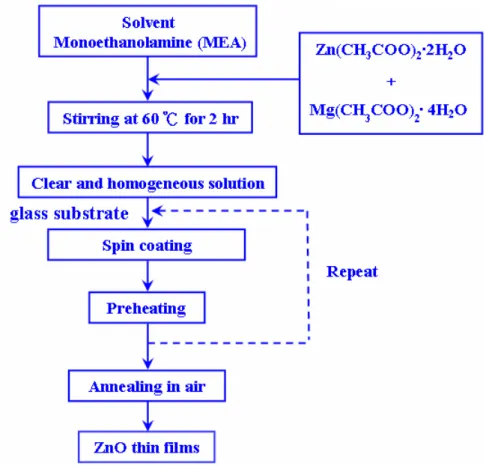
3.1.2 Synthesis of the precursors
Zinc acetate dehydrate (Zn(CH3COO)2.2H2O) is used as precursor or mixed with magnesium acetate tetra-hydrate (Mg(CH3COO)2.4H2O) were dissolved in 2-methoxyethanol, and then added monoethanolamine (MEA) to the solution. The concentration of metal ions in ZnO or Zn1-xMgxO sols were controlled between 0.375M and 0.75M, the mole ratio of Mg+2 can be varied from 0 to 0.36 (for x values); after 2 hr stirred for the mixed solution at 603!a clear and homogenous sol was obtained. The Zn1-xMgxO thin film was filmed on the alkali-free glass (Corning 1737) using spin coating method, which was under different spin speed. These as-coated films were dried at 100-1203 for 10 minutes, and then annealed at 150 to 5503
respectively for 1 hr in air atmosphere. The flow chart of the precursor preparation and ZnO films processing is showed in Fig. 3.1.
Fig. 3.1 The flow chart of the precursor preparation and ZnO films processing by spin coating.
3.1.3 Chemical bath deposition (CBD)
CBD was carried out in a beaker with a soak aqueous solution containing 0.1 mol/L zinc nitrate and 0.03 mol/L dimethylamineborane placed upon a heater-stirrer during the growth process at temperature range of 60 to 65℃. Prior to deposition, the glass substrate was activated by an industrially employed two-step Pd/Sn process using sensitizer (SnCl2, 1 g/L; 32% HCl, 1 ml/L) and activator (PdCl2, 0.1 g/L; 32%
HCl, 0.1 mol/L) [20, 21], then immersed the substrate in the soak solution for 30 min. The thickness of the ZnO film could be controlled by tuning the soak concentration or immersing time. Finally, the substrate was rinsed with DI water and dried with nitrogen gas then baked on hot-plate at 1003 for 5 min.
3.1.4 The fabrication of thin film transistor devices
The typical thin film transistors were fabricated by following procedures. All of conductive layer (source, drain, or gate electrode) was deposited by sputtering on glass substrate. Silicon dioxide or silicon nitride was served as the gate insulator with a thickness of 300nm by plasma-enhanced chemical vapor deposition (PECVD). The channel width and length were defined by photolithography. Finally, the Zn(1-x)MxO (M = Mg) thin film were deposited by solution methods with the same processes mentioned in section 3.1.1 and 3.1.2 the above.
3.2 Characterization for materials and devices 3.2.1 Scanning electron microscopy (SEM)
The scanning electron microscopy (SEM) was used the secondary electron mode to observe the morphology of ZnO materials and electronic device. The model of the SEM used here is Hitachi 4700.
3.2.2 Transmission electron microscopy (TEM)
One of the typical characters of nano-phase materials is the small object size. Although some structural features can be revealed by x-ray and neutron diffraction, direct imaging of nanomaterials is only possible using high resolution transmission
electron microscopy (HRTEM, FEI / Philip Tecnai F20). TEM is a unique technique because it can produce a real space image on the atom distribution in the nanocrystal surface. With a finely focused electron probe, the structural characteristic of a single nanomaterial can be fully understood. Normally, the chemical analysis system, the energy disperse X-ray spectrometer (EDX), was attached on TEM system.
3.2.3 X-ray diffraction spectroscopy
X-ray diffraction analysis of the ZnO specimens was carried out by using an X-ray diffractometry (XRD) (Philips PW3710 or MAC Science MAXP3) with conventional θ/2θ scans. The X-ray was generated by a Cu target (Cu Kα) operated at 50kV and 60mA, and the scanning speed was 0.02 deg/step, 1deg/min from 20° to 80°.
3.2.4 UV absorption
UV absorption was done in UV-VIS-NIR scanning spectrophotometer (SHIMADZU UV-3101PC) at wavelengths from 350 to 800 nm by employing both a tungsten-iodide (WI) lamp for the visible region and a deuterium (D2) lapmp for the ultraviolet region.
3.2.5 Thermal gravimetric analysis
Thermal weight loss was measures by thermal Gravimetric Analysis (TGA; Perkin-Elmer, thermal gravimetric analyzer 7), which is a simple analytical technique that measures the weight loss (or weight gain) of a material as a function of temperature. As materials are heated, they can loose weight from a simple process
such as drying, or from chemical reactions that liberate gasses. Some materials can gain weight by reacting with the atmosphere in the testing environment. Since weight loss and gain are disruptive processes to the sample material or batch, knowledge of the magnitude and temperature range of those reactions are necessary in order to design adequate thermal ramps and holds during those critical reaction periods.
A sample of the test material is placed into a platinum cup that is supported on, or suspended from an analytical balance located outside the furnace chamber. The balance is zeroed, and the sample cup is heated according to a predetermined thermal cycle. The balance sends the weight signal to the computer for storage, along with the sample temperature and the elapsed time. The TGA curve plots the TGA signal, converted to percent weight change on the Y-axis against the reference material temperature on the X-axis.
3.2.6 Hall effect measurement
The importance of the Hall-effect [125-127] is underscored by the need to determine accurately carrier density, electrical resistivity, and the mobility of carriers in semiconductors. The Hall-effect provides a relatively simple method for doing this. Because of its simplicity, low cost, and fast turnaround time, it is an indispensable characterization technique in the semiconductor industry and in research laboratories. It is listed as one of the most-commonly used characterization tools.
Fig. 3.2 Schematic of the Hall effect in a long, thin bar of semiconductor with four ohm contacts. The direction of the magnetic field B is along the z-axis and the sample has a finite thickness d.
The basic physical principle underlying the Hall-effect is the Lorentz force. When an electron moves along a direction perpendicular to an applied magnetic field, it experiences a force acting normal to both directions and moves in response to this force and the force affected by the internal electric field. For an n-type, bar-shaped semiconductors shown in Fig. 3.2, the carriers are predominately electrons of bulk density n. Assume that a constant current I flow along the x-axis from left to right in the presence of a z-directed magnetic field. Electrons subject to the Lorentz force initially drift away from the current line toward the negative y-axis, resulting in an excess surface electrical charge on the side of the sample. This charge results in the Hall voltage, a potential drop across the two sides of the sample. (Note that the force
on holes is toward the same side because of their opposite velocity and positive charge.) This transverse voltage is the Hall voltage VH and its magnitude is equal to
IB/qnd, where I is the current, B is the magnetic field, d is the sample thickness, and q
(1.602 x 10⁻¹⁹ C) is the elementary charge. In some cases, it is convenient to use layer or sheet density (ns = nd) instead of bulk density. One then obtains the equation
ns = IB/q|VH| (3.3) Thus, by measuring the Hall voltage VH and from the known values of I, B, and q, one can determine the sheet density ns of charge carriers in semiconductors. If the measurement apparatus is set up as described later in Section III, the Hall voltage is negative for n-type semiconductors and positive for p-type semiconductors. The sheet resistance RS of the semiconductor can be conveniently determined by use of the van der Pauw resistivity measurement technique. Since sheet resistance involves both sheet density and mobility, one can determine the Hall mobility from the equation
µ = |VH|/RSIB = 1/(qnSRS) (3.4)
If the conducting layer thickness d is known, one can determine the bulk resistivity (ρ = RSd) and the bulk density (n = nS/d)
3.2.7 Atomic force microscope (AFM)
The atomic force microscope (AFM) is a very high-resolution type of scanning probe microscope, with demonstrated resolution of fractions of a nanometer, more than 1000 times better than the optical diffraction limit. The AFM was invented by Binnig, Quate and Gerber in 1986, and is one of the foremost tools for imaging,
measuring and manipulating matter at the nanoscale. The term 'microscope' in the name is actually a misnomer because it implies looking, while in fact the information is gathered by feeling out the surface with a mechanical feeler.
3.2.8 X-ray photoelectron spectroscopy
The XPS was taken to investigate the bonding energy between each element of thin film. By absorbing a photo, an atom gains an energy amount equal to hν. It then releases an electron to regain its original stable energy state. The released electron retains all the energy from the striking photon, which can escape from the atom and keep it moving. The incident photons usually carry an energy range from 1 to 2keV by XPS analysis.
3.3 Electrical properties measurement for TFT devices
The transistor devices were analyzed with an Agilent 4155B semiconductor parameter analyzer. The Agilent 4155B Semiconductor Parameter Analyzer is an engineering instrument that allows the measurement of current-voltage characteristics of microelectronics devices and small circuits with up to eight terminals, also, the dc characterization of semiconductor devices and materials. It stimulates voltage and current sensitive devices, measures the resulting current and voltage response.
Chapter 4
Results and Discussions
4.1 Thin film transistors with active layers of zinc oxide (ZnO) fabricated by low-temperature chemical bath method
4.1.1 Descriptions
Thin film transistors (TFTs) with active channel layers of zinc oxide (ZnO) using a low-temperature chemical bath deposition have been studied. The ZnO films were fabricated on the defined-areas of bottom-gate type TFTs plate by immersing in a chemical bath containing zinc nitrate (Zn(NO3)2.6H2O) and dimethylamineborane (DMAB) aqueous solution at 60℃. Silicon oxide (SiO2) uses as the insulator. Produced TFTs plate is dried in the air at 100℃, specially, without any annealed. Capacitance-voltage (I-V) properties measured through the gate infer that the ZnO channel is n-type. Devices were achieved that Ion/Ioff ratio was more than 105, for which the channel mobility on the order of 0.248 cm2 V-1 s-1 has been determined.
4.1.2 Conceptions
Zinc oxide (ZnO), a transparent film is very popular used due to its unique optical and electronic properties in solar cells [123], photo detectors [11], light emitting devices [12], gas sensor elements [128], and surface acoustic wave guides [14]. Also, ZnO films exhibiting n-type semiconductive characteristic with wide band gap of 3.3 eV, excellent chemical and thermal stability, and can be well-oriented crystalline on various substrate, have recently been studied as the active channel
material in thin film transistors development [51, 71, 129]. Especially, the Hall effect mobility measured at room temperature for single crystals is on order of 200 cm2 V-1 s-1 [130].
Several methods are applied to prepare ZnO films, both physical and chemical deposition technologies which include sputtering [15], pulsed laser deposition [131], chemical vapor deposition (CVD) [17], molecular beam epitaxy [18], and sol-gel process [19] etc. However, most of the methods were not well suited for large area coating and low temperature processing. For the issues, chemical bath deposition (CBD) has been attracted technology which is simple and low-cost for fabricating thin film. There are many previous articles discussing the ZnO films using electroless deposition in solution bath and indicating the feasibility of low temperature [21, 23, 132-134]. These make the films good compatibility with substrate materials.
In the present article, we decided the patterning method of ZnO film, and performed the bottom-gate type TFT device with a patterned active channel ZnO film on that used CBD method. Also, the properties of films and characteristics of ZnO-TFT are studied.
4.1.3 Specifics methods
4.1.3.1 Film deposition procedure
The TFTs had a simple bottom-gate device configuration on a Corning 1737 glass substrate (Fig. 4.1 insert), where underlying ITO, 100 nm thick, was used as the gate electrode, selecting a silicon oxide (SiO2) film for the gate dielectric which thickness was 300nm, and ITO film of 100-nm as the source and drain electrodes. Each source-drain pair that was defined of a channel width W=500 μm wide and
channel length L=10 μm. The active channel pattern was fabricated using standard lithography then processed ZnO film following by CBD technique and yield TFTs after photo resist stripped (Fig. 4.1(a), (b)).
Fig. 4.1 Schematic (a) cross-sectional and (b) top view of the ZnO-based thin-film transistor.
CBD was carried out in a beaker with a soak aqueous solution containing 0.1 mol/L zinc nitrate and 0.03 mol/L dimethylamineborane placed upon a heater-stirrer during the growth process at temperatures 60 . Prior to deposition, the glass ℃ substrate was activated by an industrially employed two-step Pd/Sn process using sensitizer (SnCl2, 1 g/L; 32% HCl, 1 ml/L) and activator (PdCl2, 0.1 g/L; 32% HCl, 0.1 mol/L) [135, 136], then immersed the substrate in the soak solution for 30 min.
immersing time. Finally, the substrate was rinsed with DI water and dried with nitrogen gas then baked on hot-plate at 100℃ for 5 min.
4.1.3.2 Characterization techniques
The deposited crystal structure was identified by X-ray diffractometry (XRD) (Mac Science M18XHF-SRA) using a conventional 2θ scans over a range from 15˚ to 80˚ operated at 50KV and 200mA, the morphology was characterized by scanning electron microscopy (SEM; LEO 1530). The transistors were analyzed with an Agilent 4155B semiconductor parameter analyzer. The samples were measured in the dark.
!
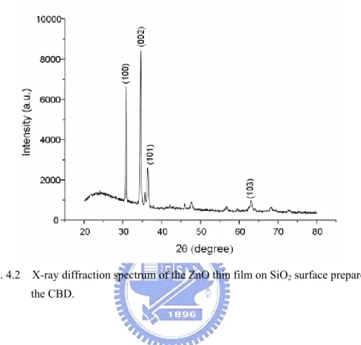
4.1.4 Achievements and explanations
The crystallographic structure of the films has been studied by X-ray diffraction. Fig. 4.2 shows the XRD spectrum of ZnO films which were deposited on the SiO2 surface of a TFT device by soaking in the aqueous solution with 0.1mol/L zinc nitrate and 0.03mol/L DMAB. The diffraction peaks (100), (002), and (101) indicate that, the produced ZnO crystals are wurtzite structure, and the morphologies consist of hexagonal column. In addition, mainly peak (002) indicates preferential c-orientation of the crystals [137], in other words that grains are mainly grown with c-axis vertical to the substrate. The regular direction growth can be explained as follows: For the electroless deposition, the crystalline morphology was led by nucleation and growth conditions. The ZnO film growing in zinc nitrate and DMAB solution followed heterogeneous nucleation [12]. However, on the SnCl2/PdCl2 pretreatment surface, the primary crystallite will prior to attack and continue to grow.
Fig. 4.2 X-ray diffraction spectrum of the ZnO thin film on SiO2 surface prepared by
the CBD.
Fig. 4.3(a) and 3(b) show the image of local ZnO film on TFT device by SEM, where are respectively cross-sectional and plane-view morphology. Hexagonal rods are observed which correspond to the basal plane of the hexagons (Fig. 4.3(a)). The ZnO film is formed of regular arrangement and compact amassment rods vertical to the substrate and the mean thickness is 400nm. As Fig. 4.3(b) shows, the grains are closely packed, that the size is largely from several ten to 200nm. For TFT application the active channel layer with larger grains size and less grain boundary can conduce to the electron mobility.
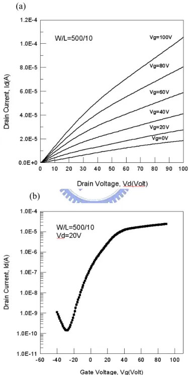
Fig. 4.4(a) and 4.4(b) show the electrical characteristics of the ZnO-TFT which the active channel layer ZnO was fabricated by CBD method without any annealed.
(a)
(b)
Fig. 4.3 SEM images of ZnO film deposited at 60℃ from 0.1 mol/L zinc nitrate and 0.03 mol/L
Capacitance-voltage (I-V) properties measured through the gate infer that the ZnO channel is n-type. Because some drain current can still be measured at 0 volt of gate voltage (refer to Fig. 4.4(a)), the device is a depletion-mode TFT. By refer to Fig. 4.4(b), the Ion/Ioff ratio was measured more than 105. The field effect mobility (μFE)
and threshold voltage (Vth) could be calculated by fitting the constant slop line to the plots of the square root of drain current vs gate voltage.
(a)
(b)
Fig. 4.4 Electrical characteristics of the ZnO-TFT which the active channel layer ZnO was fabricated by CBD method (a) Id-Vd curve, (b) Id-Vg curve.
The drain current in the saturated regions is calculated by the following equation. Idsat= μFEsat(W/2L)CI(Vgs-Vth)2
Where W and L are the channel width and length respectively, CI is the capacitance per unit area of gate insulator. The saturated regions mobility (μFEsat) was calculated of 0.248 cm2 V-1 s-1.
4.1.5 Summary
A ZnO film using for active channel layer of ZnO-TFT was fabricated by CBD in a aqueous solution containing zinc nitrate (Zn(NO3)2.6H2O) and dimethylamineborane (DMAB) aqueous solution at 60℃. The grains of the ZnO films are mainly grown with c-axis vertical to the substrate due to high participate of (002), also the ZnO crystals are hexagons (wurtzite structure). According to the present study the TFT device was successful made, it was depletion-mode and achieved that Ion/Ioff ratio was more than 105, the channel mobility on the order of 0.248 cm2 V-1 s-1 had been determined.
4.2 Cation-Mediated Effects on Zinc Oxide Films Formed by Chemical Bath Deposition
4.2.1 Descriptions
Crystalline ZnO films with a densely packed morphology were grown on a silicon oxide (SiOx) glass substrate by chemical bath deposition (CBD) in an aqueous-solution bath containing magnesium nitrate [Mg(NO3)2.2H2O] used as a cation-mediation compound, zinc nitrate [Zn(NO3)2.6H2O], and dimethylamineborane (DMAB) at 65℃. Grains of ZnO films grown in nonmediated solution preferentially grew on the (002) plane. In the cation-mediated-solution bath, the films were compressed into a compact morphology by the increased tendency for films to grow in the (002) prefer orientation. The crystalline ZnO film exhibits good optical transmittance of over 90%. Additionally, the direct band-gap value was 3.22 eV, which is less than 3.38 eV, which was obtained using a nonmediated-solution bath. This was due to the lattice constant variation caused by cation mediation.
4.2.2 Conceptions
Crystalline zinc oxide (ZnO) thin films have attracted considerable interest as a transparent conductive oxide, and exhibit n-type semiconductive characteristics with a wide band gap of 3.3 eV. Their electro-optical properties, high electro-chemical stability, large band gap, abundance in nature and absence of toxicity make them very popular for use in solar cells [123], photo detectors [11], light-emitting devices [12], gas sensor elements[143] and surface acoustic wave guides.[14]