行政院國家科學委員會專題研究計畫 期末報告
以光場增強效應提升薄膜太陽能電池吸收效率研究
計 畫 類 別 : 個別型 計 畫 編 號 : NSC 101-2218-E-009-001- 執 行 期 間 : 101 年 03 月 01 日至 102 年 09 月 30 日 執 行 單 位 : 國立交通大學電子工程學系及電子研究所 計 畫 主 持 人 : 林詩淳 報 告 附 件 : 出席國際會議研究心得報告及發表論文 公 開 資 訊 : 本計畫可公開查詢中 華 民 國 102 年 12 月 18 日
中 文 摘 要 : 本研究計畫主要是針對光電太陽能元件的光學特性之基礎研 究,其成果包括三個研究方向: (一) (一)利用周期性寬頻 高效率光場增強陣列光子晶體,提出新式太陽能電池結構, 並將光譜分離式共振腔結構應用於多接面太陽能電池上 (high-efficiency resonant-cavity-like structures for multi-junction or multi-band solar cell
application)。相對於隨機幾何繞射結構,周期性的結構可 提供可重複且較穩定的效率轉換。在這一次的計畫之中,我 們運用了表面電漿子陣列(surface plasmon array),來提供 光場增強的效應,透過在薄膜太陽能電池的上下兩端的表面 電漿子陣列。我們形成了一個共振腔結構,進而達到相當良 好的光場增強效應和效率提升。(二) 本計畫之第二個研究方 向,為進行光學特性的基礎研究,以增進對太陽能電池中, 光場增強效應(Light Trapping) 之深入了解。這一個研究之 重點 在於計算太陽能電池之光學特徵模式(eigen mode)。在 了解了特徵模式之後,在進一步研究導膜共振(guided mode resonance)之形成,和如何增強此一共振並達到寬頻增益。 (三) 進行隨機幾何形狀應用於太陽能電池底部反射鏡(back reflector) 之研究,將利用基因演算法來進行幾何形狀之最 佳化,決定最適合運用在太陽能電池的幾何形狀。在這一次 的計畫中,最佳化之隨機幾何底部反射鏡的效率,相比於週 期性陣列,可以達到~30%之提升。 本計畫的執行得到了下面的成果:(I)前瞻光學共振腔型態元 件的提案,將提供未來高效率太陽能電池的設計藍圖 (II)證 實/示範運用奈米光學模擬可以有效的提升太陽能電池的設 計,並透過有效的光場增強效應,太陽能電池的吸收與轉換 效率可以得到顯著的提升,(III)透過特徵模式的分析、透射 /反射/吸收頻譜的計算、和繞射級數的計算,提升對於太陽 能電池基礎物理的了解,尤其是光子在元件中折射/反射/繞 射的現象(IV)隨機幾何底部反射鏡之設計,將可以進一步提 升薄膜矽太陽能電池的效率 中文關鍵詞: 太陽能電池 共振腔 隨機反射鏡 特徵模
英 文 摘 要 : This research report is mainly for the fundamental research of photovoltaic device optics. The
achievement can be separated into three parts (I) Cavity-resonant solar cells using subwavelength gratings, and application of cavity-resonant structure to multi-junction cells. The specific design in this study using plasmonic effect, which
can enhance the spectral splitting through surface plasonic subwavelength grating and therefore increase the photocurrent of multi-junction cells. (II) The second effort in this proposal is the fundamental understanding of light trapping phenomenon in
photovoltaic cells. Specifically, the eigen mode and photonic bandstructure is studied, and their effect on the absorption enhancement is assessed. It should be noted that only through properly designed quasi-guided mode excitation, the thin-film solar cells can achieve their ultimate efficiency for a given active layer thickness. Other photonic enhancement
approaches such as slow light and resonance
enhancement are also preliminarily studied in this project. The last research effort of this project is (III) Improved randomized grating structures for high efficiency solar cells, through genetic algorithm optimization, and based on the physics studied in goal (II). The conventional randomly textured silver-dielectric back reflectors are widely used in
commercial solar cells. Nonetheless, well-designed random structures have not been carefully examined and not been made possible. In this project, a lithographically definable random reflector is proposed, and its efficiency is shown to be ~30% higher than its periodic counterpart.
The success of this project contribute in
(I)New/Novel/Promising optical cavity structures proposal provides directions for future high
efficiency solar cell design. (II) Demonstration of using nano photonic modeling approach to design solar cell optical structures. (III) Improving the
fundamental understanding of electrodynamic
phenomenon inside solar cells by eigen mode analysis, transmission/reflection/absorption calculation, and diffraction order analysis. (IV) Design of randomized structures benefiting future high efficiency thin-film solar cells.
英文關鍵詞: solar cell, resonant cavity, randomized reflector, eigen mode
摘要
關鍵詞: 太陽能電池 共振腔 隨機反射鏡 特徵模
本研究計畫主要是針對光電太陽能元件的光學特性之基礎研究,其成果包括三個研究方向: (一) (一)利用周期性寬頻高效率光場增強陣列光子晶體,提出新式太陽能電池結構,並將光譜分離式共振 腔 結 構 應 用 於 多 接 面 太 陽 能 電 池 上 (high-efficiency resonant-cavity-like structures for multi-junction or multi-band solar cell application)。相對於隨機幾何繞射結構,周期性的結 構可提供可重複且較穩定的效率轉換。在這一次的計畫之中,我們運用了表面電漿子陣列(surface plasmon array),來提供光場增強的效應,透過在薄膜太陽能電池的上下兩端的表面電漿子陣列。我 們形成了一個共振腔結構,進而達到相當良好的光場增強效應和效率提升。(二) 本計畫之第二個研究 方向,為進行光學特性的基礎研究,以增進對太陽能電池中,光場增強效應(Light Trapping) 之深入 了解。這一個研究之重點 在於計算太陽能電池之光學特徵模式(eigen mode)。在了解了特徵模式之 後,在進一步研究導膜共振(guided mode resonance)之形成,和如何增強此一共振並達到寬頻增益。 (三) 進行隨機幾何形狀應用於太陽能電池底部反射鏡(back reflector) 之研究,將利用基因演算法 來進行幾何形狀之最佳化,決定最適合運用在太陽能電池的幾何形狀。在這一次的計畫中,最佳化之 隨機幾何底部反射鏡的效率,相比於週期性陣列,可以達到~30%之提升。 本計畫的執行得到了下面的成果:(I)前瞻光學共振腔型態元件的提案,將提供未來高效率太陽能電 池的設計藍圖 (II)證實/示範運用奈米光學模擬可以有效的提升太陽能電池的設計,並透過有效的光 場增強效應,太陽能電池的吸收與轉換效率可以得到顯著的提升,(III)透過特徵模式的分析、透射/ 反射/吸收頻譜的計算、和繞射級數的計算,提升對於太陽能電池基礎物理的了解,尤其是光子在元件 中折射/反射/繞射的現象(IV)隨機幾何底部反射鏡之設計,將可以進一步提升薄膜矽太陽能電池的效 率。
Abstract
Keywords: solar cell, resonant cavity, randomized reflector, eigen mode
This research report is mainly for the fundamental research of photovoltaic device optics. The achievement can be separated into three parts (I) Cavity-resonant solar cells using subwavelength gratings, and application of cavity-resonant structure to multi-junction cells. The specific design in this study using plasmonic effect, which can enhance the spectral splitting through surface plasonic subwavelength grating and therefore increase the photocurrent of multi-junction cells. (II) The second effort in this proposal is the fundamental understanding of light trapping phenomenon in photovoltaic cells. Specifically, the eigen mode and photonic bandstructure is studied, and their effect on the absorption enhancement is assessed. It should be noted that only through properly designed quasi-guided mode excitation, the thin-film solar cells can achieve their ultimate efficiency for a given active layer thickness. Other photonic enhancement approaches such as slow light and resonance enhancement are also preliminarily studied in this project. The last research effort of this project is (III) Improved randomized grating structures for high efficiency solar cells, through genetic algorithm optimization, and based on the physics studied in goal (II). The conventional randomly textured silver-dielectric back reflectors are widely used in commercial solar cells. Nonetheless, well-designed random structures have not been carefully examined and not been made possible. In this project, a lithographically definable random reflector is proposed, and its efficiency is shown to be ~30% higher than its periodic counterpart.
The success of this project contribute in (I)New/Novel/Promising optical cavity structures proposal provides directions for future high efficiency solar cell design. (II) Demonstration of using nano photonic modeling approach to design solar cell optical structures. (III) Improving the fundamental understanding of electrodynamic phenomenon inside solar cells by eigen mode analysis, transmission/reflection/absorption calculation, and diffraction order analysis. (IV) Design of randomized structures benefiting future high efficiency thin-film solar cells.
一、
前言
隨著化石能源(fossil fuel)之漸漸枯竭和核能安全的問題,再生能源已成為近年來最重要之研究議 題。在所有的再生能源之中,太陽能技術是最成熟,且最有希望在近期內去取代傳統的電力產生設備, 然而,此一產業所面臨的最大問題,是 $/Watt 依然居高不下,尤其是相對於現有的發電技術,因此, 為了要使太陽能技術能普及化,降低成本與提升效率是雙軌並行的兩個重要方向。 值得一提的是,現在產學所關注的第三代太陽能電池,也即多重接面太陽能電池(multi-junction solar cells)和雜質能帶太陽能電池(intermediate band solar cells),需要大量的光學最佳化。以多接面太陽能電 池來說,其越薄的材料主動層厚度越能降低本,此在薄膜吸收不足的情形之下,光學的設計更顯重要。 儘管近幾年大量的研究被投入在太陽能電池的光學特性上,如何設計出有效的光場增強結構,如何產 生寬頻大角度以及偏振不敏感(polarization insensitive)共振腔結構的方法,依然不清楚,對於該以甚麼 參數來衡量一個太陽能電池的光學特性和設計之好壞,也尚未明朗。古時候以光軌跡長度(optical path length)來衡量太陽能電池設計的優劣,已經無法準確的描述以奈米薄膜為主的第二、三代太陽能電池, 如果可以從基礎的物理層面著手,則很有希望去發現其中的關鍵。二、
研究目的
Dielectric Mirror and Broad Angel Reflectors and Cavity-Resonant Solar Cells 介電質反
射鏡與共振腔式太陽能電池
tg tL Λ nL nH nHFig. 1 (Left) Illustration of broad band dielectric mirror and (Right) Cascaded resonant cavity type solar cell
底部反射鏡通常可以增加太陽能電池的吸收,尤其是在薄膜太陽能電池的應用上,因為材料的厚 度不夠,在長波長(紅光)的波段,必須透過底部反射鏡來增加吸收效率[1-15]。光子在進入元件之後, 如果其波長落在材料的吸收頻譜當中,就會漸漸的被材料吸收,當材料的吸收係數不夠(e.g.紅光)時, 或是材料的厚度不足時,(如薄膜太陽能電池),則大部分的光子會在經過整個元件的長度之後,而到達 元件的底部,此時,若是沒有底部反射鏡存在,則反射就只能靠半導體和空氣間的折射率差異,一大 部分的光子將進入環境(ambient)之中,而無法貢獻光電流。設計得當的底部反射鏡,可以達到 85%以 上的反射,因此是太陽能電池技術當中,不可或缺之元素。
傳統的金屬反射鏡[2, 4-6, 14],如銀、鋁、或是不鏽鋼,都可被應用在太陽能電池中。銀可以提供 高的反射係數,鋁是傳統矽製程作為導線的材料,而不繡鋼則可以作為堅固的基板(substrate)。金屬底 部反射鏡面臨的問題,包括在短波長時的低反射和高損耗(e.g. 表面電漿子吸收),因此若要將金屬反射 鏡應用在整個太陽能頻譜,是無法達到寬頻高反射的效果。當然不可否認的,金屬反射鏡依然是目前 工業化太陽能電池的主流,它有製程和設計的簡便性,尤其在設計上,金屬的沉積厚度若些許變異對 於底部反射鏡的反射能力都沒有顯著的影響,這和介電質反射鏡(dielectric mirror)必須精密控制厚度是 很不一樣的。 介電質寬頻反射鏡可以提供更高的反射[16],主要是由於它的所依賴的是折射/反射/繞射/干涉的現 象,來產生高反射結果,因而沒有如金屬會因吸收係數隨波長變化和表面電漿子吸收效應,造成在某 些波段中之低反射現象。此外,由於沒有金屬層,製程的溫度可以大幅提高,這是附帶的好處。不過 在設計上的複雜度,將比較高。尤其是如何選取對的幾何參數,將會是一個挑戰。而介電質寬頻反射 鏡相較於金屬反射鏡,有另一缺點,即介電質寬頻反射鏡通常是有方向性的,也就是說,當入射光的 波向量(wave vector)角度有所變化時,或是入射光偏振方向(polarization angle)有變化時[17],電質反射 鏡的光學特性,將會不同,因此,如何透過電磁理論計算,來得到好的低方向依賴性(low angle dependence) 的光學結構,將是未來介電質寬頻反射鏡,是否能成功應用薄膜太陽能電池上的重要關鍵。
其中一種介電質寬頻反射鏡,是所謂的分散式布拉格反射鏡(Distributed Brag Reflector),其結構為 不斷重複之交替沉積的兩種材料(ABABAB),其原理為,若是電磁波經過連續的反射,所產生的反射 波之相位皆相同時,就產生了所謂的建設性干涉,因此,整體上的反射能力,將會是很大的(>99%)。 分散式布拉格反射鏡的理論基礎是相對簡單,因此很快的被學術人士接受,且應用在多種光電元件中, 最有名的是垂直共振腔表面發射雷射(VCSEL)[7],這一光電元件的成功運作,也間接證實了分散式布 拉格反射鏡的可行性和其理論基礎。必須要點出的是,分散式布拉格反射鏡的反射能力,和材料的折 射係數差異(refractive index contrast),有很大關係,一搬來說,越大的折射率差,可以提供越高的反射 能力,且布拉格反射鏡所需要的重複組數(number of pairs)也越少,另外,由於分散式布拉格反射鏡是 一維的結構,它對於入射波的方向和偏振有較輕的依賴,這是好的,不過由於為了達到高反射能力, 往往大數量的重複組數(number of pairs)必需被沉積,這會增加元件的厚度,和製程的複雜性。
另外一種形式的介電質寬頻反射鏡,是所謂的高折射係數反差光柵結構(High Refractive Index Contrast Gratings),最早在 2004 年由 Connie J. Chang-Hasnain 提出[16]。由兩種不同的材料來組成的光 柵,由於折射係數的差異,造成很強的反射能力,而其反射能力的好壞,與兩種材料的折射係數差也 是有很大的關係,越大的差異可以造成越好的光學反應。此外,光柵的幾何尺寸,也是造成寬頻高反 射能力之關鍵,因此,對於幾何參數之設計,也是高折射係數反差光柵結構成功的關鍵。造成高反射 能力的基礎物理原因,現在還不是很清楚,一般來說,導模共振(guided mode resonance)被認為是造成 高反射現象的原因。從模擬上可以看到的高反射現象,已經從實驗上得到一些間接的映證[18-21]。傳 統的VCSEL 上下兩面必須以前面提到的分散式布拉格反射鏡,來作為雷射腔的反射鏡,由於 VCSEL 的共振腔很短(因其垂直的特質),所以其兩面的反射鏡必須具有很高的反射係數,才能達到增益(gain) 的結果,若是用布拉格反射鏡來做,則需要用約40 對的交替(pairs)才能達到高於 99%的反射,因此, 造成元件的厚度變大且製程步驟變多,若是改成光柵形式的反射鏡,則可以大大減低製程的複雜度和 元件的厚度。實驗上以光柵取代部分的分散式布拉格反射鏡,在VCSEL 上已可以看到會運作的雷射現 象。 光柵形式的反射鏡可分成一維和二維光柵,一維光柵的光學反應具有偏振的依賴性,可以用在如 量子井雷射或偏振器(polarizer)上,而二維光柵可以做到偏振不敏感,因此可以用在紅外線感測器和太
陽能電池上,值得一提的是,由於麥斯威爾方程式(Maxwell’s Equation)具可擴縮性(scalability),即: 2 2 2 2 2 2 2 2 2 ( , , ) ( , , ) ( , 0 , ) ( , , ) ( , , ) 0 E x y z E x y z E x y z x y z E x y z x y z κ ⎡⎢∂ +∂ +∂ +ω μ ⎤⎥=κ = ⎣ ∂ ∂ ∂ ε ⎦ × (1) 經過數學推導可得 2 2 2 2 2 2 2 2 2 2 2 2 2 2 ( , , ) ( , , ) ( , , ) ( ) ( , , ) ( , , ) ( / ) ( / ) ( / ) ( ', ', ') ( ', ', ') ( ', ', ') ( ') ( ') ( ') ( ) ( ', ', ') ( ', ', ') 0 E x y z E x y z E x y z x y z E x y z x y z E x y z E x y z E x y z x y z x y z E x y z κω μ κ κ κ κ κ κ κ κ κ κ κ κ κω μ κ κ κ κ κ κ ∂ +∂ +∂ + ∂ ∂ ∂ ∂ ∂ ∂ = + + ∂ ∂ ∂ + = ε ε (2) 因此,等比例的縮放可以將光柵的光學反應,在頻譜的橫軸上平移,所以,同樣的一個設計,只 要經過尺寸縮放,便可以應用在不同的波段。
Fundamental Understanding on Solar Cell Light trapping
> 100 μm, elevated $/Watt
c-Si
first generation photovoltaic
second generation photovoltaic
~ 1 μm, reduced $/Watt but insufficient
absorption,
thicker film subjects to poor charge collection
TCO
“trap” the light thin-film
Semiconductor
low cost substrate back contact
low cost substrate back reflector TCO
早期的太陽能電池,皆以矽晶圓製造為主,其厚度約在 200 μm 至 300μm 之間,這樣的太陽能電 池,有許多缺點,包括消耗掉大量的矽原料,因此價格偏高,重量偏重,且其轉換效率在非高密度太 陽能電池情形下,(即 under one sun condition),受限在 20%左右[22]。新一代的太陽能電池,將以薄膜 為主,包括矽(單晶、多晶、非結晶)、矽鍺化合物、銻化鎘(CdTe)、銅銦鎵硒(CIGS)、和各種有機化合 物等材料,因為是薄膜,對於光子的吸收並不完全,因此必需透過適當的光場增強,才能充分的利用 太陽光的能量。
傳統上來說,太陽能電池的光學特性,可以用光跡追溯技巧(ray tracing techniques)[8],和光 學軌跡長度參數(optical path length)來衡量。光跡追溯技巧的執行,是先將整個元件分割成細小網 格,光源由上往下照射,藉由簡單的折射反射定律,光在計算區域的強度分佈便可知道,這一種方法 的缺點是將光看待成純量,其電磁波的特性,也就是干涉繞射等波動現象,並不能適當地被描述。因 此,在評估傳統的矽晶圓太陽能電池上,光跡追溯技巧(ray tracing techniques),是合理有效之方 法,然而對於薄膜太陽能電池,由於光在薄膜的強烈繞射效應,更準確的電磁理論與數值方法,是達 到更高轉換效率的必要元素[3, 5, 6],此外,由於薄膜太陽能電池對光子的吸收較弱(薄膜的特性), 因此有效的光學設計,將是此新一代太陽能元件,可否能成功推行至商業化之關鍵。
值得一提的是,現在產學所關注的第三代太陽能電池,也即多重接面太陽能電池(multi-junction solar cells)[23],和雜質能帶太陽能電池(intermediate band solar cells)[22],也需要大量的光 學最佳化。以雜質能帶太陽能電池來說,其材料不論是量子點或是高度不吻合合金(Highly Mismatched Alloy),其電子擴散長度(diffusion length)皆偏短,因此元件之主動區域不能太厚,在薄膜吸收不 足的情形之下,光學的設計更顯重要。儘管近幾年大量的研究被投入在太陽能電池的光學特性上[1-6, 24-33],如何設計出有效的光場增強結構,如何產生寬頻大角度以及偏振不敏感(polarization insensitive) 結構的方法,依然不清楚,對於該以甚麼參數來衡量一個太陽能電池的光學特性和設計 之好壞,也尚未明朗。古時候以光軌跡長度(optical path length)來衡量太陽能電池設計的優劣,已 經無法準確的描述以奈米薄膜為主的第二、三代太陽能電池,如果可以從基礎的物理層面著手,則很 有希望去發現並釐清其中的關鍵。 截至目前為止,大部分的太陽能電池光學特性的研究,是比較分散的概念,一般認為對於效率提 升有幫助的現象包括了大角度的折射去增加紅外線的吸收,表面的抗反射薄膜去增加藍光的穿透,隨 機幾何的底部反射鏡去提供寬頻的散射,以及在金屬和半導體之間加入折射係數約為 2 的介電值材 料,去增加金屬底部反射鏡的反射效率,然而,這一些分散的概念,還必需要透過嚴謹的電磁理論和 模擬,才能夠真正的找出可以用來衡量太陽能電池光學效率的參數或數個參數(figure of merit),和具整 體性規劃的設計規範。
Optimized diffractive element: Random gratings
隨機幾何形狀的光學結構,在實驗上、工業應用上早已行之多年[1, 3, 5],一般來說,在沉積太陽 能電池薄膜的製程當中,就可以藉由溫度和壓力的變化,來產成顆粒大小形狀隨機分佈的表面,這個
表面就被用來當做散射太陽能光子的工具。 光子經隨機幾何形狀的結構反射,可以產生藍伯(Lambertian)分佈[7],這對於大角度的去散射光 子是很有幫助的,因此,有許多太陽能電池,使用隨機幾何的結構,作為有效的底部反射鏡,然而, 這一種隨機式的反射結構,可能會造成所生產生的太陽能電池之轉換效率,會有一定程度的變異,也 就是說,無法有效的控制樣本的品質,這對大量生產和商業化來說,是不好的因素。此外,隨機幾何 的形狀,並無經過最佳化,是否為最佳的解,並無法得到證實。 如果透過適當的設計,可以使太陽能電池的效率提升數個百分點,因而降低$/Watt,則對於太陽 能電池大眾化將會有顯著的幫助。尤其重要的是,相對於其他太陽能電池效率提升的方法,包括雜質 能帶(超高效率太陽能電池 Ultra High Efficiency Photovoltaics),有機薄膜(低價大面積),量子 結構(改變材料電性)等,光學方法和光場增強的概念,是可以被應用在任何一種太陽能電池技術(材料 架構)上的,其並無技術上的困難,未來也有機會做到不增加生產成本,而所缺少的只是理論的計算、 適當的設計、和嶄新的觀念。
三、
文獻探討
Cavity resonant type solar cell and eigen mode excitation
The use of multi-junction cells, which are occasionally referred to as tandem cells, is a practical method to exceed the Schokley and Quessier limit of photovoltaic devices. Recently, surface plasmon (SP) photovoltaics has drawn considerable attention because it can provide a new route to improve thin-film solar cell light-trapping below the diffraction limit [24, 27-31, 34-50]. The surface plasmon phenomena that have been related to photovoltaics include localized surface plasmon (LSP) [28, 29, 34, 38, 51], surface plasmon polariton (SPP) [34, 36, 37, 45, 51], and far-field enhancement. Previous studies included a single metallic nano-particle array on the top of a semiconductor layer [29, 34, 45, 52] to enhance photon forward scattering, and plasmonic back reflectors showing SPP propagation along the metal/semiconductor interface [34, 36, 37, 45, 51]. Although a single metallic grating on the top or on the bottom of the semiconductor thin-film effectively improved solar cell efficiency, cavity design is necessary to improve the efficiency even further. Here, the SP cavity design was applied to the multi-junction cells. For multi-junction cells, current matching is the most important consideration to maximize the efficiency; therefore, the subcells should have matched integrated absorbances. To optimize the geometrical parameters, a genetic algorithm (GA) was employed in this study. GA is a global search method that mimics natural evolution. It can identify a global maximum for ill-behaved objective functions, such as the optical cavity design, which is impossible to achieve using conventional optimization methods. The micromorphic silicon multi-junction cell was used as an example to demonstrate the effectiveness of GA-optimized SP cavity for spectral flux management in the multi-junction cells. Micromorphic multi-junction cells normally require a thick microcrystalline silicon (μc-Si) bottom cell due to the low absorption coefficient of μc-Si. Therefore, a surface plasmon micro-cavity can be employed to improve the absorbance of the μc-Si bottom cell and the current matching of the entire multi-junction cell.
Fundamental understanding of solar cell light trapping
Periodic grating can enhance solar cell absorbance by providing quasi-guided mode excitations[26, 30, 34, 35, 38, 40, 43, 45, 48, 49, 51, 53-55]. Nonetheless, quasi-guided modes cannot exist over the entire solar spectrum due to its discrete nature. The question arises: How to utilize the limited-number, non-continuous qausi-guided modes to maximize the short circuit current. Previously, it has been assumed that the broad band absorbance enhancement is proportional to the number of guided mode peaks[30, 54]. The work from the same authors later propose a distinction to the mode quality in terms of its overlap-integral[56]. More recent experimental work studies the dispersion and the absorption enhancement, and motivates the concept that mode confinement, i.e. Q-factor, also plays an important role in determining the broad band absorbance[53]. It is also interesting to know whether it is more efficient to use narrow band high-Q peaks or to use fewer broad band low-Q peaks, to cover a specific spectral range. In this work, it is shown that while the number of guided mode peaks has pronounced effect on the short circuit current, other factors such as the mode quality and the
mode excitation wavelength and strength also affect the short circuit current. This leads to the observation that the solar cell geometry giving the most guided modes does not coincide with the geometry giving the highest short circuit current. In this work, the solar cell geometry is optimized using global optimization algorithm[57] to maximize the short circuit current at light trapping wavelength(JSC,LT), and the resulting spectral response is
analyzed and compared. The investigation is conducted for the absorption enhancement by the non-plasmonic and plasmonic back reflectors, respectively, since the non-plasmonic and plasmonic back reflectors are expected to exhibit different natures. The optimization is repeated for several runs to confirm the result, and very similar conclusion is arrived. For non-plasmonic solar cell back reflectors, it is found that the modes are mostly of diffractive nature. The excited modes exhibit high-Q resonance and the air-dielectric-semiconductor-metal essentially acts as a conventional index-guided waveguiding structure. On the other hand, surface plasmon(SP) has long been known for its broad band emission[38, 40, 43, 45, 48, 49, 55] capability. Aaccording to the study here, the quasi-guided modes associated with plasmonic back reflectors without a dielectric spacer exhibit low-Q broad band resonances and the absorbance enhancement is mostly through the broad band coverage of solar spectrum. This is pronouncedly different from the high-Q diffractive modes for the non-plasmonic back reflectors.
Optimized diffractive element: Random gratings
Random reflectors are always of particular interest for solar cell. The optimized random geometry can potentially exceed the so-called Lambertian limit[1, 5, 7, 9, 11, 12, 14, 58-62]. There are several issues associated with optimized random geometry. (1) The optimized random profiles are usually very difficult to fabricate. (2) The randomized nature results in that the geometrical construction of conformal layers is quite difficult. The suitable geometrical definition of such a full 3D structure is inevitable, if the solar cell geometry is going to be optimized by a particular optimization algorithm. The geometry has to be adjusted automatically during optimization, rather than adjusted manually at each run. (3) The full three-dimensional(3D) solar cell structure with a random back reflector, a dielectric spacer, a conformal semiconductor layer, and a front-side anti-reflection coating has not been optimized to date due to its large computational demand.
Here a global optimization algorithm together with a geometrical parameterization procedure is proposed for designing optimal random gratings for future thin-film photovoltaics. There are several potential methods for global optimization, and genetic algorithm is selected here due to its versatility and the fact that it does not require initial guesses. The proposed method can be applied to solar cells using any materials although a silicon thin-film is used in this study. In literature, optimization of one dimensional(1D) randomized profile for solar cells has been reported [26, 33] using 2D simulation. Nonetheless, in these works the optimized 1D profile is difficult to fabricate while two dimensional(2D) grating geometry in three dimensional(3D) simulation is much preferred in real devices due to its higher absorbance enhancement. The initial result of this work can be found in [63].
四、
研究方法
Cavity resonant type solar cell and eigen mode excitation
Using multi- junction cell is a practical way to exceed Schokley and Quessier limit of photovoltaic devices. Recently surface plasmon(SP) photovoltaics draws consideration attention, which provides a new route to further improve thin-film solar cells light-trapping below diffraction limit [24, 27-31, 34-49]. This includes localized surface plamon (LSP) [28, 29, 34, 38, 51], surface plasmon polariton (SPP) [34, 36, 37, 45, 51], and photon re-emitted back into the semiconductor thin-film by surface plasmon, leading to far-field enhancement. Previous work includes a single metallic nano-particle on the top of semiconductor layer[29, 34, 45, 52], which shows enhanced photon forward scattering into silicon, and plasmonic back reflectors which in general shows SPP propagating along the metal/semiconductor interface[34, 36, 37, 45, 51]. Although a single metallic grating on top or bottom of semiconductor thin-film has been shown to be effective for improving solar cell efficiency, cavity-design is expected to improve the efficiency even further. With photonic cavity, photons can be trapped inside absorbing thin-film. In conventional thin-film photovoltaics, the trapping is due to total internal reflection (TIR) where photons outside escape cone can be totally reflected back into semiconductor thin-film. In SP cavity, absorption and remitting of photons by SP, together with LSP and SPP, can further improve the light trapping capability of photonic device, provided proper optimization can be achieved. For optimization of geometrical parameters, genetic algorithm (GA) can be used. GA is a global search method and mimics natural evolution. It can find global maximum for ill-behaved objective functions such as the case of optical cavity design. This is impossible to achieve using conventional optimization methods. The micromorphic silicon tandem cell can be used as example to demonstrate the effectiveness of GA optimized SP cavity for solar spectral flux management. Micromorphic cell normally requires thick mircrocrystalline silicon (μc-Si) bottom cell in order to have higher absorbance for long wavelength photons due to lower absorption coefficient of μc-Si. Surface plasmon microcavity canthus be employed to improve μc-Si bottom cell absorbance and current matching. Fig. 3 illustrates the two types of cavity plasmonic design including intermediate reflector and bottom grating(IRBG) cavity and top and bottom grating(TBG) cavity.
Ag μc-Si α-Si Ag Ag ZnO
Fundamental understanding of solar cell light trapping
In this work, the discretization of Maxwell’s equation is carried out by two-dimensional finite element method, using COMSOL Multiphysics software package [64]. Periodic boundary conditions are set at the left and right boundaries, while perfectly matched layer absorbing boundary conditions are used at the top and bottom boundaries of the computational domain. The absorbance in silicon is then calculated by integrating the divergence of the time-averaged Poynting vector, which is then normalized by the incident power. Only absorbance in silicon generates electron-hole while absorbance in metal leads to surface plasmon absorption loss. The details of the calculation can be found in reference[6-8, 26, 64]. The absorbance is calculated by integrating the power dissipation in silicon:
{
*}
2 0 1 ( ) 2 A( ) 1 Re ( ) ( ) ) 2 ( V S E r dv E r H r ds ε ε λ ω ′′ λ = × ⋅∫
∫
JK K JK K JJK K K (3)where ω is the angular frequency, λ is the free space wavelength, ε0 is the permittivity in vacuum, and ε″ is
the imaginary part of complex semiconductor dielectric constant. The short circuit current at light trapping wavelength, JSC,LT(600nm-1000nm) is calculated by averaging A(λ) weighted by AM 1.5 solar spectrum:
SC,LT ( )A( )
J q d
hc
λ λ λ λ
=
∫
Ω (4)where Ω(λ) is AM 1.5 solar spectrum in unit of J s-1cm-2 nm-1, h is the Plank constant, λ is the free space
wavelength, q is the elementary charge, and c is the speed of light in vacuum. The genetic algorithm is chosen as the global optimization techniques for locating the optimized geometry for the periodic grating on the solar cell back reflector. It is chosen due to the fact that the genetic algorithm has been proved to be very effective in different engineering fields[65-68]. During the optimization procedure, the objective function is defined as the short circuit current at light trapping wavelength(JSC,LT), which is to be maximized by adjusting grating
geometry. The objective value will keep increasing and then saturate, as the optimization goes on. When the optimization runs for long enough time, the objective value will gradually converge to the global maximum of the objective function. In order to reveal the relationship between the number of supported quasi-guided modes and JSC,LT, the number of qausi-guided modes for each individual(sample) is monitored during the
optimization procedure. To strengthen the conclusion, several optimization runs are conducted and highly similar result and observation are arrived, and the result is included in the following sections.
The first structure under study is a silver back reflector directly in contact with silicon. TE polarization and TM polarization in two-dimensional(2D) simulation domain are used to study the non-plasmonic back reflector and plasmonic back reflector respectively. Using TM polarization in 2D simulation domain to study the plasmonic structure has been employed [29, 34], and the structures with direct contact of metal-semiconductor are commonly referred to as plasmonic back reflectors or plasmonic structures[34, 51]. Afterward, the effect of dielectric spacer on plasmonic structures is studied to reveal the effect of dielectric
since TE polarized light does not excite surface plasmon[29, 34] and its metallic loss is much alleviated compared to TM polarization. It should be pointed out that plasmonic structures(TM) can initiate both plasmonic and non-plasmonic modes. On the other hand, non-plasmonic structures(TE) do not possess surface plasmon excitation capability.
The study is arranged as follow: Firstly the relationship between quasi-guided modes and absorption enhancement is conducted, for non-plasmonic(TE) and plasmonic(TM) back reflectors, respectively. Afterward, the usage of dielectric spacers on plasmonic structures and its effect on the optimal quasi-guided mode excitations are assessed. For the generalization to solar cells in three-dimensional(3D) domain, the non-plasmonic back reflector is more related to the solar cells with dielectric mirrors where all of the excited modes are of purely diffractive nature. For the plasmonic back reflector, it is more related to thin-film solar cells with 2D-textrued or 2D-grated metallic back reflectors. For 2D texturing/grating in 3D domain, surface plasmon absorption will exist for both polarizations. As a result, the SP absorption has to be mitigated by a dielectric spacer for both polarizations, which will be revealed later.
The film thickness is 0.3μm and poly-crystalline silicon (poly-Si) is used as an example to study different solar cell structures. For experimental poly-Si thin-film solar cell, the typical thickness is 1~2 μm. Here the thickness is kept thinner than full absorption to better reflect the light trapping effect. This is similar to Yu et al [54] where 3μm crystalline silicon is used for weak absorption while full absorption thickness of c-Si solar cells is around 200 μm. It should be emphasized that the conclusions drawn here do not only apply to poly-crystalline silicon, they also apply to other inorganic semiconductors as well. This is due to the similar mode coupling, light scattering, and waveguiding behaviors in inorganic solar cells. Crystalline silicon parameters have also been tested and the conclusion is the same except slightly lower short circuit current values. For organic solar cells, the near field enhancement is more dominant and the conclusions here may not apply. The wavelength range chosen is from 600nm to 1000nm which corresponds to the long-wavelength light trapping regime for silicon solar cells where the quasi-guided mode excitation is critical. The material refractive index and extinction coefficient is from Rsoft material database[69] and literature[9, 60, 70-73]. The CPU runtime for a single optimization run is around 72 hours using Intel quad-core Xeon 3.1GHz processor. It is worth mention that one-dimensional(1D) grating or texture is in 2D simulation domain, and 2D grating or texture is in 3D simulation domain. In the paragraph below, when 1D or 2D grating is mentioned, the specification of the simulation domain may be omitted but its meaning should be clear from the explanation above.
E
H
k
Si Ag θ ZnO:Al Ag Sik
E
H
θ ZnO:Al Fig. 4 The set-up for investigating non-plasmonic back reflectors (TE) and plasmonic back reflectors (TM) in two-dimensional space.Optimized diffractive element: Random gratings
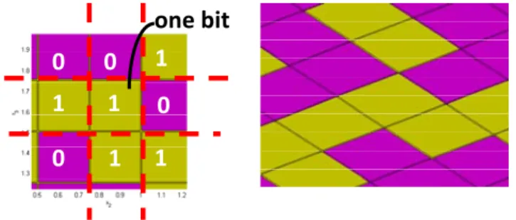
The evolutionary structure consists of ZnO/Si/ZnO/Ag, and the thickness of silicon is 700 nm, the thickness of layer 2 is 100nm, and groove height for the grating is 250 nm. The binary grating can be fabricated using usual lithography techniques in one etch step. Each binary bit is 250 nm in both width and length. The structure is defined using 7 layers. Layer 1 is a uniform Ag layer. Layer 2 is a uniform ZnO layer. Layer 3 is a ZnO/Si layer, which is defined according to the binary mask pattern as a function of 0 and 1, as shown in Fig. 5. 0 0 0 0 1 1 1 1 1 one bit
Fig. 5. (left) Illustration of the way to define layer 3 ZnO/Si and (right) 3D view.
The algorithm can be defined as below for layer 3:
if the binary mask is 1
nr=nZnO
else if the binary mask is 0 nr=nSi
(5)
1 represents the mesa and 0 represents the etched area. Therefore in (3), 1 represents ZnO while 0 represents silicon since the etched region will be conformally filled with silicon. Afterward, layer 4 is a uniform layer of silicon, whose thickness will be the total thickness minus the groove depth of the grating. Layer 5 is silicon/ZnO, and the initial binary mask can used to define the fifth layer. Layer 5 is part of the ZnO top contact conformal coverage.
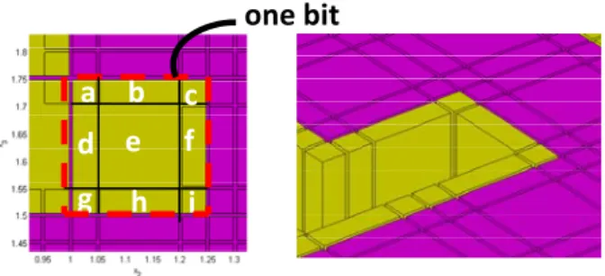
Layer 6, which is the sidewall of the top silicon grating structure, is more complicated to define. The thickness of the sidewall is 50nm, which is assumed to be half of the film thickness of the topmost ZnO coverage. As illustrated in Fig. 6, the side wall definition can be done by dividing one bit of binary mask pattern into 9 sub-regions. Whether each sub-region should be air, silicon or ZnO is determined by whether its adjacent region is silicon or air and whether the underlying binary mask bit is 0 or 1. In addition, for each sub-region, the situation can be slightly different as stated below.
e d g a h b c f i one bit
Fig. 6. (left) Illustration of the way to define layer 6 sidewall and (right) 3D view.
For the case of sub-region a, b, c, d, f, g, h, or i, if the underlying binary mask bit is 1, a ZnO grating bump is already defined in the layer 3 at this specific mask bit location. Thus in order to achieve conformal coverage, silicon refractive index is used. In the case that the underlying binary mask bit is 0, which means at this specific mask bit location a ZnO grating dip is already defined in layer 3, the sub-region in the layer 6 should be air or ZnO, depending on whether any of the adjacent regions is silicon or not. If any of the adjacent regions is silicon then ZnO refractive index is used since the sub-region in this case should be the ZnO sidewall of the adjacent silicon material.
if the binary mask is 1
nr=nSi
else
if one of the adjacent region is silicon nr=nZnO
else
nr=nair
(6)
For sub-region e, the situation is simpler. If the underlying binary mask bit is 1, which means a ZnO grating bump is already defined in this specific mask bit location in layer 3, silicon refractive index is used to construct the conformal coverage of silicon thin-film. Otherwise if the mask bit is 0, air refractive index is used.
if the binary mask is 1
nr=nSi
else
nr=nair
(7)
Layer 7 is the topmost ZnO front contact coverage, which constitutes part of the top ZnO conformal coverage. The thickness of the layer 7 ZnO coverage is 100nm. The definition can be extended from layer 6 using the same sub-region method as depicted in (4) and (5). Material optical constants can be found in literature [9, 70, 71, 73-77].
五、
結果與討論
Cavity-resonant type solar cell and eigen mode excitation
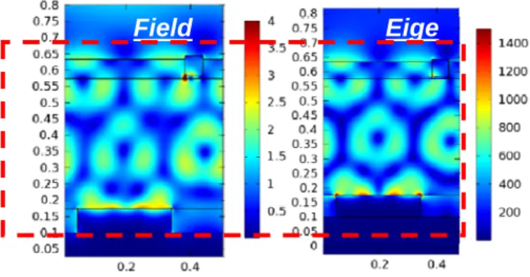
Fig. 7 Example of (Left) Field profile for scattering problem and corresponding (Right)Eigen mode.
Fig. 7 shows an example cavity resonant type solar cell where the similarity between field profile of scattering problem and eigen mode problem exists. SP single grating has been shown to be effective when placed on top of semiconductor thin film or above metal back reflectors. Nonetheless, the combined structure with both top and bottom grating that enables optimal cavity design has not been investigated. Here two type of cavity, i.e., plasmonic intermediate reflector & bottom grating(IRBG) and plasmonic top & bottom grating (TBG) are proposed and their capability to improve absorbance is studied. For SP intermediate reflector & bottom grating, structure consists of Ag back reflector/Ag&ZnO bottom grating/μc-silicon thin-film/ Ag intermediate reflectors/ α-Si thin-film, for SP top & bottom grating, structure consists of Ag back reflector/Ag bottom grating/μc-silicon thin-film/ α-Si thin-film/ Ag top grating. The optimization is done by adjusting each geometrical parameter until highest absorbance is found. Poynting vector and absorption power density which characterizes incident power per unit area and absorbed power per unit volume respectively can be written as
poynintg absorption ( ) ( ) ( ) ( ) P E r H r P E r J r = × = ⋅ JK K JJK K JK K JK K (8)
The electromagnetic field is essentially a time-varying field and time-averaged quantity is of interest as far as calculation of absorbance is concerned. The Poynting theorem, under harmonic steady state, states that time-averaged inflow power equals the time-averaged absorbed power.
{
}
{
}
absorption, avg poynintg,
* avg * 1 1 Re ( ) ( ) Re ( ) ( ) 2 (λ) 2 0 V S V S P dv P d S E r σ E r dv E r H r d S + ⋅ = ⋅ + × ⋅ =
∫
∫
∫
∫
JK K JK K JK K JK K JJK K JKv
v
(9)where σ is conductivity of materials. The absorbance is the fraction of power absorbed divided by incident
power which is solar spectrum.
{
}
{
}
* * 1 Re (λ) ( ) ( ) 2 ( ) 1 Re ( ) ( ) 2 E r E r dr A E r H r d S σ λ = ⋅ × ⋅∫
∫
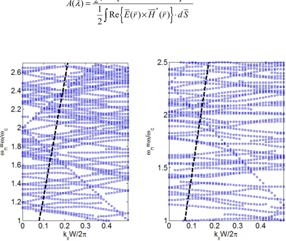
JK K JK K K JK K JJK K JK (10)Fig. 8 Example of Line cone(black line) and photonic bandstructure for (Left)IRBG and (Right)TBG cavity-resonant type solar cell Fig. 8 shows the photonic band structure for two types of cavity resonant solar cell. The frequency is normalized according to
n / c / EG, α-Si
ω ω ω= = =ω (11)
where ωc is the cutoff wavelength of tandem cell which is taken to be 1000nm here. Bloch theorem states that
photons in periodic structure can propagate without scattering and thus the photon lifetime can be extended if geometry is optimized. The photonic bandstructure can be utilized to observe quasi-guided mode excitation [28, 42, 46]. For any incident angle, a line can be drawn to characterize the relationship between ω and kx:
0sin θ=
= sin θ
x
k k ω με (12)
where kx is in-plane wavevector, k0 is wavevector in vacuum, ω is angular frequency, μ and ε is permeability
and permittivity, and θ is incident angle. The corresponding incident field is
Z,0 0 0
( , ) exp( xsinθ- cosθ)
inc j y
HK x y =H jk k (13)
The intersection between the line (Eq.(9)) and the photonic bandstructure is where quasi-guided mode excitation is likely to exist. The line cone corresponds to incident angle of 90° and the y-axis corresponds to normal incidence. The Bloch periodic wave function in the SP cavity is
P
( ) ( ) exp( )
H rK K =H rK K jk rK&⋅K (14) where k|| is in-plane wavevector and HP is periodic modulation. The eigen mode excitation condition can be
written as:
0sin
kK& =k θ (15) which means in-plane component of incident wavevector matches Bloch wavevector.
Another point that can be revealed by photonic bandstructure is slow light enhancement. It can be seen from Fig. 8 that the photon group velocity is significantly lower than the phase velocity especially at bandedge such as Γ point at long wavelength portion. The group velocity characterizes the electromagnetic wave propagation in the film and it can be expressed as:
( ) g k v k ω ∂ = ∂ (16)
The group velocity is related to the slope of photonic bandstructrue. In cavity the propagation of electromagnetic wave is no longer plane wave of infinitely extent and the photonic density of state (PDOS) is modified. Properly tailored and optimized cavity will lead to enhanced solar cell absorbance due to modified density of state and extended photon cavity lifetime.
Fundamental understanding of solar cell light trapping
Ag
ZnO:Al
Si
Highest Absorbance
Highest Absorbance
Ag
ZnO:Al
Si
0.6 0.7 0.8 0.9 1 0 0.2 0.4 0.6 0.8 Wavelength (μm) A b so rb a n ce Si Absorbance Metal Absorbance 0.6 0.7 0.8 0.9 1 0 0.2 0.4 0.6 0.8 Wavelength (μm) A b so rb a n ce Si Absorbance Metal AbsorbanceD
C
B
A
H
G
F
E
ZnO:Al
ZnO:Al
t
dsFF¯
Λ
Λ
h
gt
frontt
dsFF¯
Λ
Λ
h
gt
frontk
E
H
k
E
H
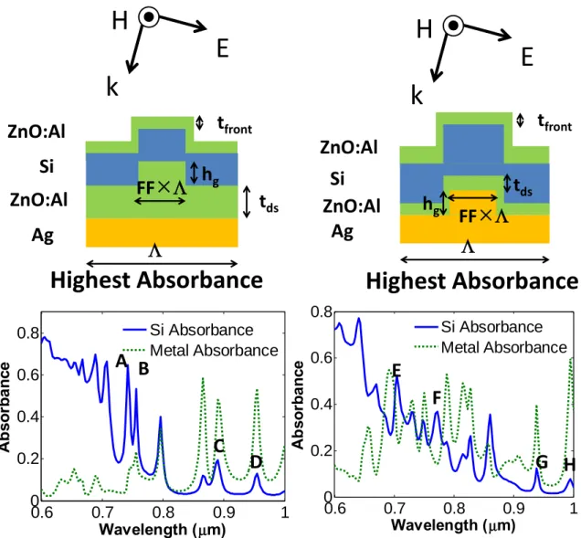
Fig. 9 The highest short circuit current spectral response for the dielectric-spaced plasmonic back reflectors after optimization for (left) the grating on the dielectric-spacer(GDS) structure and (right) the grating on the silver(GS) structure.
From previous sections, it is seen that the absorbance enhancement by the purely plasmonic back reflectors without a dielectric spacer is significantly lower than the non-plasmonic diffractive back reflectors ones due to metallic absorption. To improve the silicon absorption by reducing metallic absorption, the JSC,LT
is now calculated for dielectric-spaced structures and the geometry optimization is carried out for the grating period(Λ), fill factor(FF), grating height(hg), incident angle(θ), and dielectric spacer thickness(tds), as
illustrated in the drawing of Fig. 9. In theoretical papers, there are two types of structure exist for dielectric spaced plasmonic back reflectors[33, 42]: one is grating on the dielectric spacer(GDS) [33] and the other is grating on silver(GS) [42]. The GDS structure is illustrated on the left in Fig. 9 where the grating is etched on the dielectric spacer and the silver-dielectric spacer interface is mostly flat. The GS structure is illustrated on the right in Fig. 9 where a grating is formed on the silver surface and then a conformal dielectric spacer layer is deposited on silver. In experiment, GS structure is mostly conducted, and the practice is texturing the silver
back reflector before depositing the subsequent layers. Therefore the experimental structure is more similar to the grating on silver(GS) structure. Nonetheless, it is going to be shown that the GS structure is less efficient then the GDS structure at their respective optimized geometry, due to the lower metallic absorption of the GDS structure. For GDS structure, the optimized geometry is Λ=0.4684μm, FF=0.3548, hg=0.198μm,
tds=0.144μm, and θ=7.0866°. For GS structure, the optimized geometry is Λ=0.548μm, FF=0.2471,
hg=0.187μm, tds=0.25μm, and θ=4.7244°. tfront is fixed at 80nm for both structures. The optimized highest
short circuit current at light trapping wavelength, JSC,LT, is 7.6387 mA/cm2 for the grating on dielectric
spacer(GDS) structure, and 7.1617 mA/cm2 for the grating on the silver(GS) structure, which are all higher
than the case without the dielectric spacer for the purely SP back reflectors without a dielectric spacer in Section 4 (JSC,LT=6.3399 mA/cm2). The improvement in JSC,LT for GDS structure is 20.49%, compared to SP
back reflectors without a dielectric spacer.
It should be pointed out that the number of excited quasi-guided modes also shows increase as the optimization proceeds, but the optimization still does not converge to the geometry that leads to the most supported modes. In order to keep the paper concise, the statistics for the optimization is not shown here again for the dielectric-spaced structures. Repeated global optimization run is also conducted, and similar results are arrived. Therefore, the optimized geometry giving the highest short circuit current does not coincide with the geometry leading to the most quasi-guided modes. Surface plasmons are still excited at specific wavelengths although it is of much weaker strength compared to the plasmonic back reflector without a dielectric spacer. The excitation of surface plasmons(SP) in dielectric spaced structures is due to the incomplete shielding of the dielectric. The metallic absorption is effectively reduced and the optimized trade-off between SP excitation and SP absorption leads to higher silicon absorbance. Therefore, for the plasmonic back reflectors in inorganic solar cell structures, direct contact of metal-semiconductor, such as the case in section 4, tends to result in increased metallic absorption and is not a preferable way for light trapping. While near field SP effect can be extremely effective[34, 43] in organic devices, the far field SP light scattering by SP back reflectors in inorganic semiconductor can be significantly degraded by metallic absorption. The metallic loss is especially detrimental if a whole metallic back reflector is directly in contact with the semiconductor[51], compared to the case where only small nano-scale metallic particles are placed at the front or the rear side of the devices[78]. While a lot of SP structures with metal back reflectors directly in contact with inorganic semiconductor is conducted[35, 51], it is suggested here that the conventional dielectric spaced back reflector is still more efficient for long-wavelength light trapping, due to the balance between SP assisted absorption enhancement and metallic absorption loss. Surprisingly, it is also found that the grating on the dielectric spacer(GDS) itself is more effective than the grating on the silver(GS) back reflector, different from the experimental practice were the metallic back reflectors are textured before the subsequent depositions. The higher JSC,LT is mainly because the GS structure tends to lead to more metallic absorption, evident from the
spectral response in Fig. 9.
Since in reality the two-dimensional texture or grating is mostly used for solar cells, the excitation of surface plasmon exists for both TE and TM polarizations. It is therefore suggested that for solar cells with metal back reflectors, dielectric spacer should be included and the texture should be formed the dielectric spacer itself. In the cases where dielectric mirrors are employed, high-Q diffractive modes should be utilized
cells still employ metal back reflectors, non-plasmonic back reflectors, such as dielectric mirrors, can potentially provide higher photocurrent due to lower SP absorption loss.
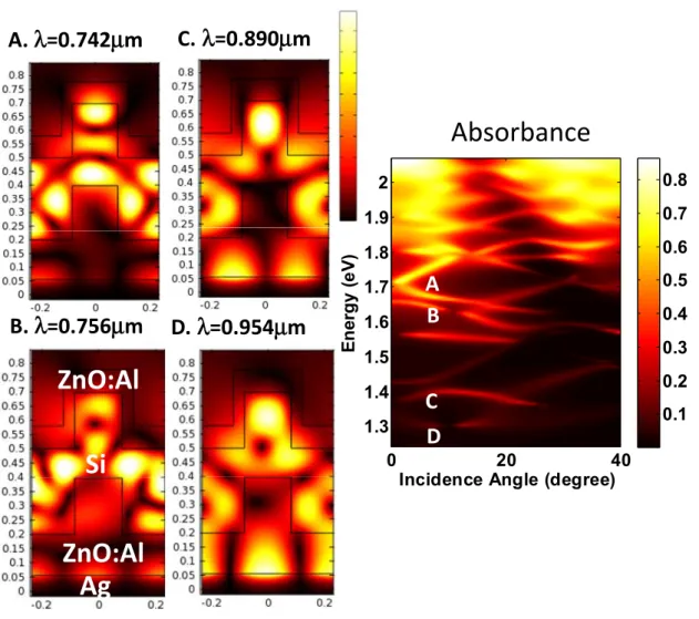
Incidence Angle (degree)
En er g y ( e V) 0 20 40 1.3 1.4 1.5 1.6 1.7 1.8 1.9 2 0.1 0.2 0.3 0.4 0.5 0.6 0.7 0.8
A.
λ=0.742μm
B.
λ=0.756μm
C.
λ=0.890μm
D.
λ=0.954μm
D
C
B
A
Ag
ZnO:Al
Si
ZnO:Al
Absorbance
Fig. 10 (Left) the field profiles at the quasi-guided mode peak wavelengths for the optimized grating on the dielectric spacer(GDS) structure. (Right) the corresponding photonic bandstructure.
Incidence Angle (degree) En er g y ( e V ) 0 20 40 1.3 1.4 1.5 1.6 1.7 1.8 1.9 2 0.1 0.2 0.3 0.4 0.5 0.6 0.7 0.8
E.
λ=0.705μm
F.
λ=0.769μm
G.
λ=0.938μm
H.
λ=0.995μm
H
G
F
E
Ag
ZnO:Al
Si
ZnO:Al
Absorbance
Fig. 11 (Left) the field profiles at the quasi-guided mode peak wavelengths for the optimized grating on the silver(GS) structure. (Right) the corresponding photonic bandstructure.
Fig. 10 and Fig. 11 show the field profiles and the photonic bandstructures of the optimized geometry, for both GDS and GS dielectric-spaced structures. It can be seen from Fig. 9 that in spectral responses some of the quasi-guided mode peaks are accompanied by the elevated metallic absorption while the other peaks are not. The enhanced field intensity at metal-silicon interface at the long wavelength in Fig. 10(λ=0.954μm) and Fig. 11(λ=0.995μm) further confirms the excitation of surface plasmons. The quasi-guided mode excitation is also labeled in the photonic bandstructure at the right of Fig. 10 and Fig. 11. The Bloch wavefunction for a periodic structure can generally be written as
{
}
( , ) Re ( ) exp( Bloch ) exp( )
E r tG G = u rG G −jkG ⋅rG jωt (17)
where E is the electric field, kBloch is the Bloch wavevector, ω is angular frequency, t is the time, and u is
the periodic modulation. The condition for the excitation of the qausi-guided modes is
0sin 0 0sin Bloch
k θ =ω με θ =kG (18)
where k0 is the free space wavevector of the incident field, μ0 and ε0 is the free space permeability and
permittivity respectively, and θ is the incidence angle as illustrated in Fig. 4. It should be pointed out that here the x-axis in the photonic bandstructure is θ rather than kBloch, and the conversion between them is also
The slope of the photonic band structure is the photon group velocity: 1 0 1 cos Bloch Bloch dk d d d dk dθ d d k ω θ θ θ ω⎛ ⎞− ω = ⎜ ⎟ = ⎝ ⎠ (19)
Although the slow light enhancement is not the main point of this paper, it is still worth to point out that at the quasi-guided mode wavelengths, the photon group velocity is significantly slower than its free space phase velocity and therefore the enhanced absorbance can be achieved.
Optimized diffractive element: Random gratings
The calculation of Poynting vector, energy loss, and integrated quantum efficiency can be referred to literatures[7, 8, 26, 64]. The calculated integrated absorbance, AInt, is 0.7380 for the optimized geometry and
0.5697 for its periodic counterpart. The optimized grating geometry is shown in Fig. 12. The spectral response is shown in Fig. 13 where a 4X4 quasi-random grating provides 23% broad band improvement compared to its 2D periodic counterpart. At short wavelength, the optimized structure shows broad band improvement due to the transmission enhancement, as is clear in the insect of Fig. 13. At long wavelengths, the Fabry-Perot type resonances are seen in the 2D-periodic grating due to the quasi-guided mode excitations.
(a)
(b)
Fig. 13. Spectral responses for (a) the 2D periodic grating and (insect) the transmission at the front surface (b) the optimized 4X4 quasi-random grating and (insect) transmission at the front surface.
The Lambertian absorption limit is[79]:
4 2 4 (1 ) [1 (1 A( ) ] 1/ ) W W e n e α α λ − − − − − = (20)
where α is the absorption coefficient, n is the semiconductor refractive index, and W is the film thickness. Although at the resonance frequencies the absorbance of the baseline cell with 2D periodic gratings can exceed the Lambertian limit in (6) at certain wavelengths, the broad band enhancement is not as strong as the optimized random structure. The well-defined quasi-guided-modes in the periodic grating make it possible to exceed the Lambertian limit. Nonetheless, at wavelengths other than the resonances, the absorbance is much lower. Since it is difficult for guided modes to exist over the entire solar spectrum, a comprised but optimized random grating can provide higher overall efficiency. Planar cell in general shows wave interference characteristics at the short wavelength where peaked absorbance is seen when wave impedance is matched for the thin-film solar cell stack. It shows weak absorption at long wavelength due to insufficient light scattering, resulting from the lack of large angle diffraction.
penetrating from air into silicon is plotted. Retaining only the front surface texture is a common practice for calculating anti-reflection characteristics[35]. Since there is no back reflector, no quasi-guided mode is excited and therefore in the transmittance curve very few peaks are observed. At the long wavelength portion of the solar spectrum, the transmission is essentially very high due to the matched wave impedance. The impedance matched condition for the ZnO front contact assuming planar structure is:
ZnO ZnO ZnO 4 2 m n t n λ + λ = (21)
where λ is the free space wavelength, nZnO is the ZnO refractive index, and m is non-negative integer. For
the 2D-perioidic grating the transmission is further improved at all wavelengths where a broad band transmission is observed instead of perfect transmission at a single wavelength, as is the case for the planar structure. The lower transmission at the short wavelength for both insects in Fig. 13(a)(b) is due to two factors. First is directly from (7). nZnO is approximately equal to 2 and tZnO =100nm, and thus the first impedance
matched point is around λ=800nm, and the second is λ=266.67 nm. Since there is no impedance matched point around λ=400nm-600nm, the transmission is lower at short wavelength. The second reason is that the imaginary part of dielectric constant (εr”) becomes higher at short wavelength, which in turn lowers the
transmission. The transmission peak around λ=448.5nm is unlikely the result of impedance matching since there is no such points in this spectral range. It is more likely due to the strong waveguiding effect where the ridged-geometry guides the incident wave into the silicon slab. The further broad band transmission improvement of the random grating over the 2D periodic grating is due to its optimized geometry.
[1] H. Sai, et al., "Light trapping effect of submicron surface textures in crystalline Si Solar Cells," Prog. Photovolt. Res. Appl., vol. 15, pp. 415–423, 2007.
[2] S.-S. Lo, et al., "Broad-band anti-reflection coupler for a : Si thin-film solar cell," J. Phys. D: Appl. Phys. , vol. 40, pp. 754–758 2007.
[3] C. Haase and H. Stiebig, "Thin-film silicon solar cells with efficient periodic light trapping texture," Appl. Phys. Lett., vol. 91, p. 061116, 2007.
[4] H. Stiebig, et al., "Silicon thin-film solar cells with rectangular-shaped grating couplers," Prog. Photovolt. Res. Appl., vol. 14, pp. 13–24, 2006.
[5] H. Stiebig, et al., "Light trapping in thin-film silicon solar cells by nano-textured interfaces," in Photonics for Solar Energy
Systems, Strasbourg, France, 2006, p. 619701.
[6] C. Haase and H. Stiebig, "Optical properties of thin-film silicon solar cells with grating couplers, design and fabrication of submicron grating structures for light trapping in silicon solar cells," Prog. Photovolt. Res. Appl. , vol. 14, pp. 629–641, 2006. [7] P. Bhattacharya, Semiconductor Optoelectronic Devices, 2nd Ed. Upper Saddle River, NJ: Prentice-Hall, 2006.
[8] Synopsys, "Sentaurus Device EMW User Manual V. X-2005.10," ed, 2005, pp. 78-79.
[9] V. Shah, et al., "Thin-film silicon solar cell technology," Prog. Photovolt. Res. Appl. , vol. 12, pp. 113–142 2004.
[10] N. Senoussaoui, et al., "Thin-film solar cells with periodic grating coupler," Thin Solid Films vol. 451–452 pp. 397–401, 2004.
[11] J. Krc, et al., "Potential of light trapping in microcrystalline silicon solar cells with textured substrates," Prog. Photovolt. Res.
[12] S. S. Hegedus and R. Kaplan, "Analysis of quantum efficiency and optical enhancement in amorphous Si p–i–n solar cells,"
Prog. Photovolt. Res. Appl. , vol. 10, pp. 257–269 2002.
[13] T. Brammer, et al., "Optical properties of silicon-based thin-film solar cells in substrate and superstrate configuration," Sol.
Energ. Mat. Sol., vol. 74, pp. 469– 478, 2002.
[14] A. Shah, et al., "Photovoltaic technology: the case for thin-film solar cells," Science, vol. 285, pp. 692-698, 1999.
[15] M. T. Gale, et al., "Design and fabrication of submicron grating structures for light trapping in silicon solar cells," in
Proceedings of SPIE, Conference on Optical Materials Technology for Energy Efficiency and Solar Energy Conversion IX, 1990, pp.
60-66.
[16] C. F. R. Mateus, et al., "Ultrabroadband mirror using low-index cladded subwavelength grating," IEEE Photon. Tech. Lett., vol. 16, pp. 518-520, 2004.
[17] R. Magnusson and M. Shokooh-Saremi, "Physical basis for wideband resonant reflectors," Optics Express, vol. 16, pp. 2456-3462, 2008.
[18] M. C. Y. Huang, et al., "A nanoelectromechanical tunable laser," Nature Photonics, vol. 2, pp. 180-184, 2008.
[19] X. M. Zhang, et al., "Variable nano-grating for tunable filters," in The 14th International Conference on Solid-State Sensors,
Actuators and Microsystems, Lyon, France, 2007, pp. 2417-2420.
[20] M. C. Y. Huang, et al., "A surface-emitting laser incorporating ahigh-index-contrast subwavelength grating," Nature Photonics, vol. 1, pp. 119-122, 2007.
[21] S. Boutami, et al., "Broadband and compact 2-D photonic crystal reflectors with controllable polarization dependence," IEEE
Photon. Tech. Lett., vol. 18, pp. 835-837, 2006.
[22] Schokley and Queisser, "Detailed balance limit of efficiency of p-n junction solar cell," J. Appl. Phys., vol. 32, pp. 510-519, 1961.
[23] R. R. King, et al., "40% efficient metamorphic GaInP/GaInAs/Ge multijunction solar cells," Applied Physics Letter, vol. 90, p. 183516, 2007.
[24] D. Cheyns, et al., "The angular response of ultrathin film organic solar cells," Appl. Phys. Lett., vol. 92, p. 243310, 2008. [25] K. Knop, "Reflection grating polarizer for the Infrared," Opt. Commun., vol. 26, pp. 281-283, 1978.
[26] A. Lin and J. D. Phillips, "Optimization of random diffraction gratings in thin-film solar cells using genetic algorithms," Sol.
Energ. Mat. Sol., vol. 92, pp. 1689-1696, 2008.
[27] A. Meyer and H. Adea, "The effect of angle of incidence on the optical field distribution within thin film organic solar cells,"
J. Appl. Phys., vol. 106, p. 113101, 2009.
[28] W. E. I. Sha, et al., "Angular response of thin-film organic solar cells with periodic metal back nanostrips," Opt. Lett., vol. 36, pp. 478-480, 2011.
[29] M. Yang, et al., "Incident angle dependence of absorption enhancement in plasmonic solar cells," Opt. Express, vol. 19, pp. A763-A771, 2011.
[30] Z. Yu and S. Fan, "Angular constraint on light-trapping absorption enhancement in solar cells," Applied Physics Letter, vol. 98, p. 011106, 2011.
[31] S. B. Mallick, et al., "Optimal light trapping in ultra-thin photonic crystal crystalline silicon solar cells," Optics Express, vol. 18, pp. 5691-5706, 2010.
[32] B.-J. Kim and J. Kim, "Fabrication of GaAs subwavelength structure (SWS) for solar cell applications," Optics Express, vol. 19, pp. A326-A330, 2011.