國 立 交 通 大 學
電子工程學系 電子研究所碩士班
碩 士 論 文
二氧化鉿經四氟化碳電漿處理後應用於有機薄
膜電晶體之研究
The Study of HfO
2dielectric by CF
4plasma treatment for OTFT
application
研 究 生:曾 憶 雯
指導教授:張 國 明 博士
二氧化鉿經四氟化碳電漿處理後應用於有機薄
膜電晶體之研究
The Study of HfO
2dielectric by CF
4plasma treatment for OTFT
application
研 究 生:曾憶雯 Student:Yi-Wen Tseng
指導教授:張國明 博士 Advisor:Dr. Kow-Ming Chang
國 立 交 通 大 學
電子工程學系 電子研究所碩士班 碩 士 論 文
A Thesis
Submitted to Department of Electronic Engineering ﹠Institute of Electronics College of Electronic Engineering and Computer Science
National Chiao- Tung University in Partial Fulfillment of the Requirements
for the Degree of Master of Science
In
Electronic Engineering July 2009
Hsinchu, Taiwan, Republic of China
二氧化鉿經四氟化碳電漿處理後應用於有機薄
膜電晶體之研究
研究生:曾憶雯 指導教授: 張國明 博士 國立交通大學 電子工程學系 電子研究所碩士班 摘 要 電子束蒸鍍系統的優點是可以將製程溫度控制在 200℃以下,適合應用於軟 性電子製程,但若無經過高溫熱退火,長出的薄膜較鬆散且缺陷多,故用 CF 電 漿來處理此薄膜。在這次研究中,採用的介電層是 Hf0 ,我們成功的利用”氟” 的修補降低了介電層的漏電。因 Hf0 屬於高介電係數(k~24)材料,我們可以提 高電容值進而降低臨界電壓,使薄膜電晶體的操作電壓降到~-2 伏特。相比於只 用爐管通氮氣 150℃一小時,CF 電漿處理的電性較好,而經過 CF 電漿處理再 加上沉積 HMDS 2 分鐘的電性比沒有沉積 HMDS 的好。 4 2 2 4 4 iThe Study of HfO
2dielectric by CF
4plasma treatment for OTFT
application
Student:Yi-Wen Tseng Advisor:Dr. Kow-Ming Chang
Department of Electronics Engineering and Institute of Electronics
National Chiao Tung University, Hsinchu, Taiwan
ABSTRACT
The advantage of E-Gun Evaporation System is that we can control the process temperature to be under 200 ℃, and that is suitable for the application of flexible electronic process. The thin films are loose and defective if they are not annealing with high temperature, so usually we use CF plasma display panel to process the thin film. In the research, we use HfO as the
4
2 dielectric layer and successfully reduce
the electric leakage by using fluorine to mend the dielectric layer. Because HfO is a high dielectric material (k~24), we can advance the capacitor value to level down the threshold voltage and lower the operation voltage of thin-film transistor to -2V. In comparison with processing with furnace and add N in it for one hour, the electronic characteristic of thin film through CF
2
2
4 plasma treatment is better. The
electronic characteristic of thin film through CF 4 plasma treatment deposits HMDS for 2 minutes is better than not depositing HMDS.
誌 謝
首先,我要感謝指導老師張國明教授在碩士兩年研究中給予我熱心的指導。 老師對於學問中強調嚴謹的探討數據及探究其理論機制,讓我在實驗方法和實驗 態度上有很大的成長。在此獻上最深的謝意。 其次,要感謝實驗室的各位學長,給予我課業和實驗上的建議。特別是菘宏 學長,在實驗過程中給予我很多的幫助,提醒我無論是製程或量測都需注意很多 的小細節,使我的實驗能順利完成。對於學長兩年來的照顧,我將永記於心。 另外,實驗室的同學,給予我碩士班許多的歡笑。無論是在修課或實驗,大 家都一起努力、一起檢討、一起排解實驗地苦悶,這種同甘共苦的日子,我會永 遠珍藏。 謝謝交大奈米中心和國家奈米實驗室提供各種的機台設備,讓我可以順利進 行我的實驗。 最後,我要感謝我的父母對我從小到大的栽培,還有我姐姐總在我心情低落 或感到迷惘時給予我鼓勵和開導,讓我能順利完成學業。 iiiContents
Chinese Abstract……….………..……….i
English Abstract………..……….ii
Acknowledgement ( in Chinese )………..………..iii
Contents………...……….iv
Table Captions………..……… ..vi
Figure Captions…………..………....vii
Chapter 1 Introduction
1-1 Introduction of organic thin film transistor……….……….………...…..11-2 Organic semiconductor material………..………..1
1-2-1 Classified the organic semiconductor materials….………...….3
1-2-2 Characters of pentacene……….………...……..4
1-3 Gate dielectrics………...5
1-3-1 High-k inorganic………...…..……5
1-3-2 Polymer………..…..…...6
1-3-3 Self-assembled small molecules………..………...…6
1-3-4 Inorganic /polymer stacked………..……..7
1-3-5 Characters of hafnium oxide……….……….……7
1-4 Device structure………...……..8
1-5 Organic thin film transistor operating mode………..……....8
1-5-1 Source/Drain contact…….……….8
1-5-2 operating mode……….…..9 iv
1-5-3 Important parameters……….………...…10
1-5-3-1 Field effect mobility…..……….………….10
1-5-3-2 Threshold voltage……...……….……….…...11 1-5-3-3 OFF ON I I ratio……….…..11 1-5-3-4 Subthreshold swing……….………..…..12
Chapter 2 Experiment
2-1 Hafnium oxide deposited with E-gun and CF plasma treatment on the metal insulator metal (MIM) structure………...….194 2-1-1 Different bottom electrode……….……...19
2-1-2 Different bias of HDPCVD system……….….…20
2-1-3 Different process time……….…..…20
2-2 Fabricated processes of organic thin film transistor……….………...21
2-3 ICP system………...………....22
Chapter 3 Results and Discussion
3-1 hafnium oxide dielectric layer quality analysis and appraisal on MIM structure………...…..31
3-1-1 Different bottom electrode………..32
3-1-2 Different bias of HDPCVD system………32
3-1-3 Different process time……….………34
3-2 OTFT electric characteristics analysis and discussion………...35
Chapter 4 Conclusion and Future work
4-1 Conclusion………...……50
4-2 Future work………..……51
Reference………...……
52 vTable Caption
Chapter 3
Table 3-1 The capacitance density and EOT of Ni/HfO /different bottom
electrode MIM……….38
2
Table 3-2 The capacitance density and EOT of of Ni/HfO /Ni bottom electrode MIM with different process time of CF plasma treatment………...44
2 4
Table 3-3 The electronic characterization of OTFT………..………48
Figure Caption
Chapter 1
Fig. 1-1 formation of polaron………13 Fig. 1-2 chemical structure of some p-type organic semiconductors pentacene, 6T,
P3HT, F8T2, PTAA, PVT, DH-5T, DH-6T………..13 Fig. 1-3 chemical structure of some n-type organic semiconductors BBB, QM3T, NTCDI………..14 Fig.1-4 semilogarithmic plot of the highest field-effect mobilities(μ ) reported
for OTFTs fabricated from the most promising polymeric and oligomeric semiconductors versus year from 1986 to 2000………….14 Fig.1-5 X-ray diffractograms schematic representatios of structural order, and
field-effect mobilities corresponding to three different thin film pentacenes. (a) An amorphous phase is achieved using a substrate temperature. -196Tsub = ℃ and a deposition rate. (b) A single “thin film phase” resulted for Tsub =27℃ (c) Setting ℃ yielded a film consisting of two phases the “thin film phase” and the “single crystal phase”………...15
55 Tsub =
Fig.1-6 chemical structure of some polymers used as OTFT dielectrics PVP, PS, PMMA, PVA, PVC……….….16 Fig. 1-7 Schematic of organic thin film transistor (OTFTs) with horizontal of (a)
bottom contact structure (b) top contact structure (c) vertical structure...16
Fig. 1-8 Band diagram of semiconductor and metal. (a) n-type semiconductor and low work function metal (b) p-type semiconductor and high work
function……….17
Fig. 1-9 Metal work function for a clean metal surface in a vacuum versus atomic number………..17
Fig. 1-10 Schematic of organic thin film transistor (OTFTs) on accumulation mode……….……18
Fig. 1-11 Schematic of organic thin film transistor (OTFTs) on operating mode...18
Chapter 2
Fig. 2-1 Fabrication flow of different bottom electrode MIM structure (a) Ni bottom electrode (b) Pd bottom electrode (c) TaN bottom electrode (d) Al bottom electrode………..23
Fig. 2-2 Fabrication flow of different bias MIM structure………..……..25
Fig. 2-3 Fabrication flow of different process time MIM structure………..……27
Fig. 2-4 Fabrication flow of organic thin film transistor (OTFT) before the surface treatment………..28
Fig. 2-5 HfO2 treated with O2 one hour by furnace……….…..29
Fig. 2-6 HfO2 treated with CF4 plasma ICP=500W, bias=10W, time=90S, temperature=150℃, pressure=100mTorr……….29
Fig. 2-7 HfO2 treated with CF4 plasma ICP=500W, bias=10W, time=90S, temperature=150℃, pressure=100mTorr and then added HMDS 2 min………29
Fig. 2-8 Deposited pentacene on OTFT’s HfO2 dielectric layer………...30
Fig. 2-9 Source/ drain patterned on pentacene……….30
Fig. 2-10 Schematics of the ICP high density plasma system……….……30
Chapter 3
Fig. 3-1 SEM image of HfO (a) without treatment, (b) with CF plasma treatment……….…...…...37
2 4 Fig. 3-2 The electronic leakage current characterization of HfO with CF plasma treatment and different bottom electrode……….…38
2 4
Fig. 3-3 The electronic leakage current characterization of Ni/HfO /Ni bottom electrode MIM with different bias of CF plasma treatment………..………....39
2 4
Fig. 3-4 Graph of XPS analysis of “F 1s” of HfO /Ni bottom electrode………..39 2 Fig. 3-5 Graph of XPS analysis of “C 1s" of HfO2/Ni bottom electrode……40
Fig. 3-6 Graph of XPS analysis of “Hf 4f" of HfO2/Ni bottom electrode…...41
Fig. 3-7 Graph of SIMS analysis of Ni/HfO /Ni bottom electrode ………...…..42 2 Fig. 3-8 The electronic characterization of HfO /Ni bottom electrode MIM with
different bias of CF plasma treatment for C-V………...42
2 4
Fig. 3-9 AFM surface image of HfO2 (a) without treatment which roughness is 0.596nm, (b) with CF plasma treatment which roughness is 0.515nm………..……….43
4
Fig. 3-10 The electronic leakage current characterization of Ni/HfO /Ni bottom electrode MIM with different process time of CF plasma treatment………..………44
2 4
Fig. 3-11 AFM surface images of the treated with (a) annealing at 150℃ 1 hour , (b) treated with CF plasma , and (c)
treated with CF plasma +HMDS and then deposited pentacene which areas are 2 HfO N2 2 HfO 4 HfO2 4 m 1 m 1 and m 5 m 5μ × μ μ × μ ………...…..45
Fig. 3-12 The electronic characterization of OTFT for (a) annealing 1 hour (b) CF plasma treated (c) CF plasma +HMDS treated gate dielectric……….…..46
DS DS-V
I N2
4 4
Fig. 3-13 The electronic characterization of OTFT for IDS vsVGS………...…47 Fig. 3-14 The electronic characterization of OTFT for log10
( )
IDS -VGS..………..47 Fig. 3-15contact angle of the treated with (a) annealing at 150℃ 1hour, (b) treated with CF plasma, and (c) treated with CF plasma +HMDS………...49 2 HfO N2 2 HfO 4 HfO2 4
ix
Chapter 1
Introduction
1-1 Introduction of organic thin film transistor
The first OTFT invented by Tsumura. A, at 1986. [1] Comparing with traditional Si semiconductor, OTFT had the possibility of avoiding expensive systems of high vacuum, high temperature; low cost process, ability of large area application, and flexibility, etc.. The inorganic semiconductors’ molecule-molecule are bonded by covalent bond, however the organic semiconductors are almost bonded by Van der Waals forces and coulomb force, and the interaction of them are weak, so the mobilities are apparently lower than inorganic semiconductor a few orders( Si crystal was 300~900 cm2/V-S and pentacene was ~1 cm2/V-S). Furthermore, the thin films consist of organic molecules which are solid, but they still can be seen as the extremely low temperature liquid. So, the stable of devices are bad.
Due to the characters of organic semiconductor, the OTFT have been used in various applications in displays and flexible electronic devices, such as biochemical sensors, liquid-crystal flat panel displays, radio-frequency identification (RFID), etc. Although OTFT had been studied for many years, but there’re still space we can devote to, such as improving the mobility, output current, operation speed, and lowering the operation voltage.
Compared with traditional thin film transistor, the OTFT using organic materials instead of inorganic materials. In the past, we described electrical characteristics of the materials through energy band diagram theory. And energy band theory emphasized the periodicity and directivity of substances. Because of the characters between conductor and insulator, inorganic semiconductor can be applied widespread. In energy band theory, the vanlance band of semiconductor filled, but it has a smaller energy band gap (~1ev). In the room temperature, electrons thermal inject into conduction band, and obtain the character of electric conduction. Nevertheless, organic semiconductors can conduct electricity because the conjugate structures of molecule main chains have resonance phenomenon, which cause reciprocal overlapping, and resulted in a continuous molecular orbit, and made π -electrons moving free. Therefore, when analysing the charges transmission, we should consider the characters of molecule, lattice structure, and solid state. [2] In order to explain the conductor phenomenon of the organic semiconductors, we borrowed the polaron and bipolaron theory from physics, since 1980.
On solid state, the polarons are formed by a charge carrier appeared on ionic lattices. Figure 1-1[3] shows the hole carrier would attract the negative ion and repulse the positive one, which makes some positive ions delocalize on some molecule chains[3]. When the main chains of the conjugate molecules are cut off on structure defect, and then produced a new energy state that higher than vanlance band. It just like, an electron moved from a filled band bonded molecule orbit would improve the energy state. Generally speaking, polaron is not the main electric conduction mode. Namely, the polarons cannot let electrons transmit from band to band.
When an electron move from an oxidative molecule which contains polaron, two conditions may happen. One is this electron moves from another chemical bond of
molecule chain and then produces a polaron, the other is the electron moves from the previous polaron’s energy band and then creates a more stable bication, which is called bipoaron. The bipolaron then was might only transmit the electrons from band to band.
Generally speaking, conjugate molecules produced polarons on low doping concentration, and produced bipolarons on high doping concentration. If there are more bipolarons, the energy would overlap on energy band edge, and produced a narrower bipolaron energy band between the energy bands. [4]. The Figure 1-4 is the field effect mobility of organic semiconductors from 1986 to 2000.
1-2-1 Classified the organic semiconductor materials
Organic semiconductors, considered the forms, we can divide them into small molecules and macro-molecules; considered the majority-carriers types, we can divide them into p-type and n-type. P-type materials are transmitting holes, usually include pentacene, 6T (sexithiophene), P3HT (regioregular poly [3-hexylthiophene], F8T2 (poly [9,9’ dioctyl-fluorene-co-bithiophene]), PTAA (polytriarylamine), PVT (poly [2,5-thienylene vinylene]), DH-5T ( α,ω -dihexylquinquethiophene), DH-6T (α ,ω-dihexylsexithiophene), etc, which are shown in Figure 1-2[5] . Among them, pentacene and 6T are small molecules. For small molecules we adopt evaporative method to deposit because they’re hard to dissolve. Besides small molecules, the rest of them are macro-molecules. For the macro-molecules materials we usually use spin coater to deposit, in order to make them easier to dissolve, we add some substituents on these macro-molecules’ main chain. For example, we spin P3HT by adding chloroform(CCl ). 4
[bisbenzimidazobenzophenanthroline]), QM3T (3’, 4’-dibutyl-5, 5”-bis (dicyanomethylene)-5, 5”-dihydro-2, 2’: 5’,-2”-terthiophene), NTCDI (naphthalene tetracarboxylic diimide) etc, which are shown in Figure 1-3[5]. QM3T, NTCDI are small molecules.
Presently, most of organic semiconductors’ LUMO( lowest unoccupied molecular orbital) are higher, which keeps electrons injected from electrode, and makes the mobility of holes larger than electrons’. As a result, the OTFT now are almost p-type. Fig.1-4 showing the field effect mobilities of organic semiconductors.
1-2-2 Characters of pentacene
Pentacene ( ) is a polycyclic aromatic hydrocarbon that contains five benzene rings. It’s molecular weight is 278.3, and the length of its C-H bonds is calculated as~1.096 Å, and the length of its C-C bonds vary from 1.35 to 1.44 Å[6], As mentioned in the introduction, the structure contains conjugate double bonds (
14 22H
C
π-bonds) because of the benzene rings, so the band gap is 1.85eV[7], which is very close to semiconductor. Therefore, pentacene possess the ability of transmit carriers. The pentacene, with single-crystal phase, it’s hole mobility is 3.2 , and electron mobility is 2.0 in room temperature (RT). However, with the thin-film phase( polycrystal structure), it’s hole mobility is 0.3~1 .
S -/V cm2 S -/V cm2 S -/V cm2
In Figure 1-5[8], the growing form of pentacene depends on temperature very much. By growing amorphous films of pentacene, which keeps the substrate temperature close to -196℃ during deposit, and the film is practically insulated because of its the disorder characters in the solid. When substrate temperature is keeping in RT during the deposit, a very high ordered film is deposited and then we
got high mobility of 0.6 . When the mixture of the thin film phase and the single-crystal phase is grown, the mobility is very low, and that possibly may because the coexistence of two phases causes high defective concentration.[8][9][10] The thickness of pentacene also affects the field effect mobility. The OTFT with thinner pentacene layers display higher hole mobilities probably because thinner channel forms shorter source-drain transport path for holes. The optimum thickness is about 30nm, or it will cause high leakage current. [11]
S -/V cm2
Now, many researchers try to improve the field-effect mobility of pentacene-based thin film transistors: chemical treatment on dielectric film surfaces, modification of the TFT structures, and manipulation of the pentacene deposit processes, etc.[11]
1-3 Gate dielectrics[12]
In fact, the mobility of the carriers of organic semiconductors now have approached or surpassed the amorphous Si (mobility of amorphous Si ~0.1 cm2/V-S). To achieve that, we need very large operation voltage, even if lager than 30-50V. The large operation voltage will lead to excessive power consumption. A large capacitance of dielectric layer can drive the device with a lower bias. Therefore, there are many researches in dielectric layer of the OTFT. We describe dielectric layer into four classes, that is high k inorganic, polymer, self-assembled small molecules and inorganic/polymer stacked.
1-3-1 High-k inorganic
has relatively low dielectric constant (k=3.9) and substantial tunneling currents when extremely thin films are employed. The use of suitable high-k materials
2
can obtain greater capacitance values. That means the interface of semiconductor/ dielectric has a greater surface charge density. Under the same capacitance values, larger insulator thickness has lower leakage currents. As Vth = φms – Qtot/Cox – Qdep/Cox
+ 2φF. We can get low Vth, when the oxide capacitance density(Cox=ε0k/tox)increased.
As the
(
)
( )
( )
ln( )
10 C C C 1 q kT 10 ln q mkT V I log V/dec S OX it dep -1 G D 10 × ⎟⎟ ⎠ ⎞ ⎜⎜ ⎝ ⎛ + + = × = ⎥ ⎦ ⎤ ⎢ ⎣ ⎡ ∂ ∂ =when we have greater capacitance values, we get lower subthreshold swing (SS). The [12], [13], [14], [15] are common dielectric materials for OTFT to reduce the operation voltage.
3 2O
Al TiO2 HfO2 TaO2
1-3-2 Polymer
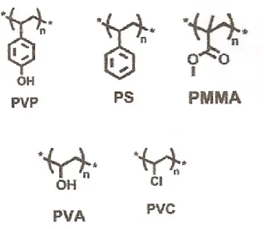
Gate dielectrics which are solution-processable materials are often formed simply by spin-coating, casting, or printing in room temperature and under ambient conditions. The organic semiconductor materials deposit on polymer dielectric layer easier. The polymer materials can also add the adhesion to organic active layer. But the leakage current of polymer dielectric may large because it is not easy to deposit uniform. So, the polymer dielectric layer deposit thicker and the Vth is large. Figure
1-3 shows common polymeric dielectric materials such as PVP (polyvinylphenol), PS (polystyrene), PMMA (polymethylmethacrylate), PVA (polyvinylalcohol), PVC (polyvinylchloride).
1-3-3 Self-assembled small molecules
smaller than 3nm. The reason for being an efficient insulting barrier is its high tunneling barrier height. The values were found to be independent of the film thickness. Tunneling barrier height of a densely packed SAM of n-alkyltrichlorosilanes (thickness range 1.9-2.6) is 4.5eV for charge carrier[16], which is greater than 3nm SiO2(~3.2eV). The SAM is usually use to passivant on dielectric layer.
1-3-4 Inorganic/polymer stacked
The high k dielectric layers are thicker, (compared with SiO at the same capacitance) to avoid serious gate leakage current. However, it has highly hydrophilic surface which is not compatible with the growth of organic semiconductors, because that may cause undesirable interactions with organic semiconductor. On the other hand, the major selling point of ultrathin organic gate dielectric is the hydrophobic and smooth surface which is suitable for stacking organic semiconductor. But it also has a demerit. During the deposit, there’re pinholes in organic film because of the imperfections in the structure. Now we can stack the organic layer on the high k layer to circumvent the drawbacks and use the benefits of both gate materials.[17]
2
1-3-5 Characters of hafnium dioxide
In the future, thin films were widely investigated as a potential high-k oxide in replace of in silicon microelectronics. It can not only reduce the threshold voltage to near zero for pentacene-based TFTs, but also the thickness of the gate insulator to nanometer. The pentacene grown on the . The grain size of pentacene increases significantly compared with those grown on ,which may
2 HfO 2 SiO 2 HfO 2 SiO
improve the field effect mobility of OTFT.[18] It has high dielectric constant (k=22~25 for high temperature process) and high band gap (Eg=5.7 eV) [14]
The interface states of high-k dielectric are similar to those of gate dielectric. Oxygen vacancies in the HfO
2
SiO
2 are formed in the deposit itself or oxygen
redistribution during high-temperature processes, which lead to shallow defect sites with single- or double-charged states and traps the electrons.[19] Fluorine may be the best passivant for defects in ionic oxide because it is the only element that is more electronenegative than “O” and for its bond length is similar. That means metal-F states will always tend to lie outside of the oxide band gap.[20]
1-4 Device structure
Usually, test structures of OTFT are fabricated in several modes. Ordinarily, we could divide into two kinds, such as horizontal and vertical, which showing as Figure 1-7. The advantages of top contact are fine source/drain resolution, more planar surface to deposit pentacene and good contact resistance, and the disadvantage is contaminated pentacene by patterned source/drain. The bottom is contrary to top contact.
1-5 Organic thin film transistor operation mode
1-5-1 Source/Drain contact
Ideally, the electrodes of source/drain should be ohmic contact with majority-carriers of organic semiconductors. There are two methods to produce an
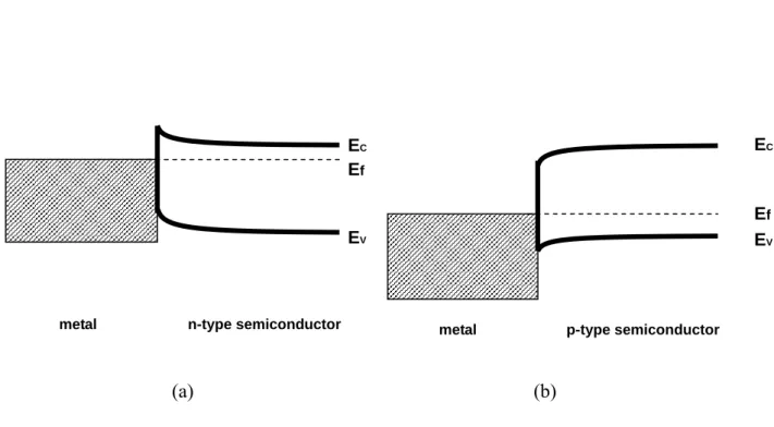
ohmic contact. First, we can increase the doping concentration of semiconductors. Second, find an appropriate mental to match. For example, in Figure 1-8, n-type semiconductors need a low work function metal and p-type semiconductors need a high work function metal. That make majority carriers “see” a lower barrier height, and than improve the mobility.
We chose pentance, which was p-type, to be our organic semiconductor, so higher work function metal was our priority selection to treat as source/drain electrodes. According to Figure 1-9, we considered over Au (work function~5.47eV) to be the source/drain electrodes.[21][22]
1-5-2 Operation mode
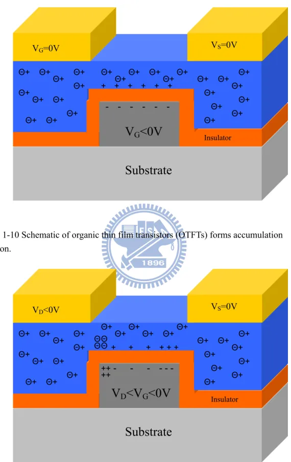
Organic semiconductors usually operate on accumulation mode. Take p-type pentacene –based as the example. In Figure 1-10 VD =VS =VG =0, If we increase the negative voltage of VG gradually, and the negative voltage will go across the dielectric layer and will be close to the interface of dielectric and semiconductor. Positive charges accumulate on the interface of dielectric and semiconductor which causes the semiconductor energy band bending and forms a positive charges channel. The channel is an accumulation region. The positive charges come from ohmic contact of source and drain. On the contrary, when negative charges increase on interface of dielectric and semiconductor, positive charges deplete which makes the band bending inversely. After the accumulation region was formed, we add a negative
D
V and make VS=0, VG <VD <0. The positive charges which approach drain reduce. The loss of voltage on the channel verse the position in the channel is a function. When the negative voltage in VD is higher thanVG. As in Figure 1-11, the
positive charges will be depleted in drain and create a depletion region. The OTFT is on saturation state.
Organic semiconductors have less choices to form an inversion mode. That is because an organic semiconductor has a larger band gap in comparison with Si, the velocity of thermal induce carriers is lower than Si. Also, Carries injection in source/ drain is not ohim contact.
1-5-3 Important parameters
Organic thin film transistor usually discusses several parameters, such as mobility, threshold voltage,
OFF ON
I
I ratio and subthreshold swing.
1-5-3-1 Field effect mobility
On the influence of electric field, the transmission ability of electron or hole in the semiconductor is mobility. Theoretically, there are two methods to calculate it. First, lower drain voltage on the linear region, drain current is add linear with the drain voltage. We can use the:
D D th G i d V 2 V -V -V L WC I ⎟ ⎠ ⎞ ⎜ ⎝ ⎛ = μ (1-1) If we calculate ∂ID/∂VG, we can get a transconductance gm:
i D const. V G D m V L WC V I g D μ = ⎟⎟ ⎠ ⎞ ⎜⎜ ⎝ ⎛ ∂ ∂ = = (1-2)
We measurement the low drain voltage of ID versus VGgraph, and the slope of the curve is gm . Substitute the W, L,Ci, and VD, and than get the mobility.
Second, when VD bigger than VG which on saturation region, the accumulation layer in the drain will generate pin-off. The current satisfied
i
(
G th 2 D V -V 2L WC I = μ)
(1-3) We drafting the 2 1 DI versus VG graph, the slope is μ 2L WCi
. Substitute the W, L, andCi, and than get the mobility.
1-5-3-2 Threshold voltage
The gate voltage higher than threshold voltage is the base condition to driver device. The interface state between semiconductor and dielectric may trap the charges, when the charges transmitting and thick dielectric layer both need larger threshold voltage to drive device.
Two methods to obtain the V .th
First, when operator on linear region, which based on equation (1-1), measure ID versus VG curve with VS=0, low VD, and than get a maximum gm. Make a tangent at VG, which at maximum gm. The tangent line cut the VG axis, and the intersection point is 2 V V V D th
G = + . Substitute the, VD and than get the V .th
Second, when on saturation region, which made square root on equation (1-3). And obtain i
(
G th D V -V 2L WC I = μ)
(1-4) We can find the curve cut the VG axis is the V .th1-5-3-3 OFF ON I I ratio
ION express the channel current when transistor on the accumulation region, and the IOFF express on the depletion region. The larger ratio shows that the device easier to control and the performance is better. Measure ID versus V G curve,
OFF ON
I
I ratio is the maximum / minimum ratio.
D
I ID
1-5-3-4 Subthreshold swing
Subthreshold swing always indicates the quality of the interface between dielectric and semiconductor. To subthreshold swing, the smaller value is better. Define the subthreshold swing which is
(
)
( )
( )
ln( )
10 C C C 1 q kT 10 ln q mkT V I log V/dec S OX it dep -1 G D 10 × ⎟⎟ ⎠ ⎞ ⎜⎜ ⎝ ⎛ + + = × = ⎥ ⎦ ⎤ ⎢ ⎣ ⎡ ∂ ∂ = (1-5)Draft ID versus VGcurve. Make the log
( )
ID versus VG plot, there is a linear region. The inversion of slope is the subthreshold swing.+ - + + + - + - - + - + + + - + - - Hole carrier
Fig. 1-1 Formation of polaron[3]
Fig. 1-2 Chemical structure of some p-type organic semiconductors pentacene, 6T, P3HT, F8T2, PTAA, PVT, DH-5T, DH-6T.[12]
NTCDI
Fig. 1-3 Chemical structure of some n-type organic semiconductors BBB, QM3T, NTCDI.[12]
Fig.1-4 Semilogarithmic plot of the highest field-effect mobilities(μ) reported for OTFTs fabricated from the most promising polymeric and oligomeric semiconductors versus year from 1986 to 2000.[24]
Fig.1-5 X-ray diffractograms schematic representatios of structural order, and field-effect mobilities corresponding to three different thin film
pentacenes. (a) An amorphous phase is achieved using a substrate
temperature. -196Tsub = ℃ and a deposition rate. (b) A single “thin film phase” resulted for Tsub =27℃ (c) Setting Tsub =55℃ yielded a film consisting of two phases the “thin film phase” and the “single crystal phase” [8]
(a)
(b)
Fig.1-6 Chemical structure of some polymers used as OTFT dielectrics PVP, PS, PMMA, PVA, PVC.[12] Source Drain Insulator Gate Substrate Active layer Drain Source
Active layer Insulator
Gate Substrate (a) (b) Substrate Drain Insulator Gate Active layer Source (c)
Fig. 1-7 Schematic of organic thin film transistors (OTFTs) with horizontal of (a) top contact structure (b) bottom contact structure (c) vertical structure.
Evac
metal n-type semiconductor
EV
EC
Ef
metal p-type semiconductor
EV
EC
Ef
(a) (b)
Fig. 1-8 Band diagram of semiconductor and metal. (a) n-type semiconductor and low work function metal (b) p-type semiconductor and high work function.
Fig. 1-9 Metal work function for a clean metal surface in a vacuum versus atomic number.[21][22]
V
G<0V
Substrate
- - - + + + + + + Θ+Θ+ Θ+ Θ+ Θ+ Θ+ Θ+ Θ+ Θ+ Θ+ Θ+ Θ+ Θ+ Θ+ Θ+ Θ+ Θ+ Θ+ Θ+ Θ+ Θ+ Θ+ Θ+ Θ+ Θ+ Θ+ VG=0V VS=0V InsulatorFig. 1-10 Schematic of organic thin film transistors (OTFTs) forms accumulation region.
V
D<V
G<0V
Substrate
++ - - - - - - Θ+ Θ+ Θ+ Θ+ Θ+ Θ+ Θ+ Θ+ Θ+ Θ+ Θ+ Θ+ Θ+ Θ+ Θ+ Θ+ Θ+ Θ+ Θ+ Θ+ Θ+ Θ+ Θ+ Θ+ Θ+ Θ+ VD<0V VS=0V + + + + + + Θ Θ Θ Θ ++ InsulatorFig. 1-11 Schematic of organic thin film transistors (OTFTs) on saturation state of accumulation mode.
Chapter 2
Experiment
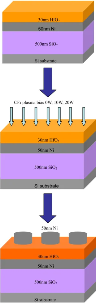
2-1 Hafnium dioxide deposited with E-gun and CF
plasma
treatment on the metal insulator metal (MIM) structure
4
In this scenario, we purpose to deposit hafnium dioxide dielectric on the bottom el ectrode metal by E-gun technology. In order to conform with flexible substrate, all the process, except the thermal oxide, need low temperature (< 200 ). ℃
First, the n-Si (or p-Si) wafer was used as the substrate, and was rinsed in the deionization water (DI water), and then dipped in dilute HF solution (HF:DI water =1:100) , that to remove the native oxide. The wafer was accomplished the RCA clean procedure after, and use furnace at 1000 , one hour to deposit silicon dioxide ℃ 500nm thick on the top of n-Si (or p-Si) substrate for isolation purpose. And the next step we choice three conditions to discuss:
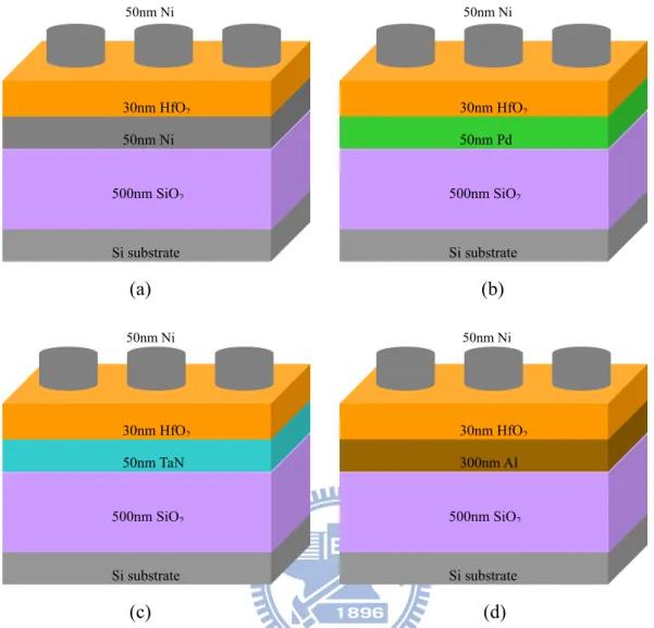
2-1-1 Different bottom electrode
As shown in Figure 2-1, used E-gun to deposit 50 nm nickel (Ni), 50 nm palladium (Pd), and used sputter to deposit 50 nm tantalumnitride (TaN), 300 nm aluminum(Al) on 500 nm SiO individually. And then we used E-gun to deposit the hafnium dioxide(HfO
2
2) 30 nm as the dielectric layer on the bottom contact at 150 . ℃
The next step was using HDPCVD to add CF4 plasma treatment in order to improve the electrical properties of dielectric. The deposition source CF flow rate was 100 4
sccm, ICP power was 500 W, bias was 0 W, process pressure was 100 mTorr, and process time was 90 sec, temperature was150 ℃.
Finally, all top contact electrodes were deposited 50 nm thick Ni layer defined as shadow mask by E-gun. The active region pad of etch capacitors’ area was 4×10⁻⁴/cm . 2
2-1-2 Different bias of HDPCVD system
As shown in Figure 2-2, we used E-gun to deposit 50 nm Ni on 500 nm SiO . And then we used E-gun to deposit the HfO
2
2 30 nm as the dielectric layer on the
bottom contact at 150 . The next step was using HDPCVD ℃ to add CF plasma treatment in order to improve the electrical properties of dielectric. The deposition source CF flow rate was 100 sccm, ICP power was 500 W, process pressure was 100 mTorr, process time was 90 sec, temperature was 150 ℃ and bias was 0 W, 10 W, 20 W individually. Finally, all top contact electrodes were deposited 50nm thick Ni layer defined as shadow mask by E-gun. The active region pad of etch capacitors’ area was 4×10
4
4
-4/cm2.
2-1-3 Different process time
As shown in Figure 2-3, we used E-gun to deposit 50 nm Ni on 500 nm SiO . And then we used E-gun to deposit the HfO
2
2 30 nm as the dielectric layer on the
bottom contact at 150 . The next step was using HDPCVD ℃ to add CF plasma treatment in order to improve the electrical properties of dielectric. The deposition source CF flow rate was 100 sccm, ICP power was 500 W, process pressure was 100 sccm, ICP power was 500 W, bias was 0 W, process pressure was 100 mTorr,
4
temperature was 150 ℃ and process time was 30, 90, 150 sec individually. Finally, all top contact electrodes were deposited 50 nm thick Ni layer defined as shadow mask by E-gun. The active region pad of etch capacitors’ area was 4×10⁻⁴/cm . 2
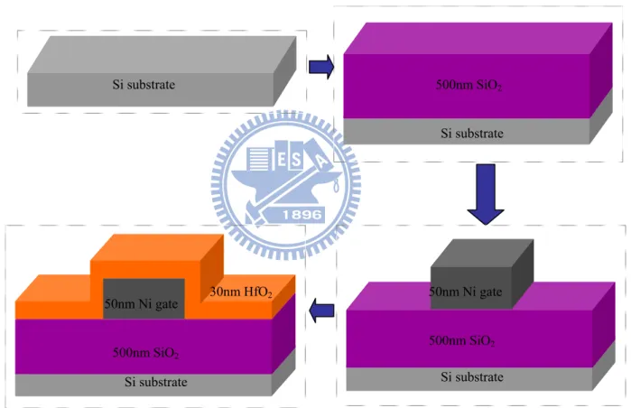
2-2 Fabricated processes of organic thin film transistor
In this scenario, we chose the better CF plasma condition to treatment on the 30 nm insulator as gate dielectric layer on the organic thin film transistor structure.
4 2
HfO
As shown in Figure 2-4, the n-Si (or p-Si) wafer was used as the substrate, and was rinsed in the deionization water (DI water), and then dipped in dilute HF solution (HF:DI water =1:100) , that to remove the native oxide, the wafer was accomplished the RCA Clean procedure after, The wafer was accomplished the RCA clean procedure after, and use furnace at 1000 , one hour to ℃ deposit SiO2 500 nm thick on the top of n-Si (or p-Si) substrate for isolation
purpose. The bottom contact structure was adopted to fabricate organic thin film transistor.
And we deposited 50 nm thick Ni layer as the gate electrode by lift-off method. The Ni layer was deposited by E-gun and HfO2 30nm deposited by E-gun. In order to
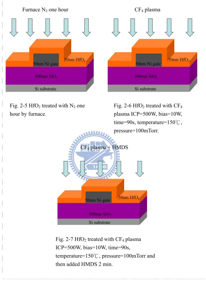
compare the electronic characteristics of OTFT, we adopted three treatments on dielectric layer:
As shown in Figure 2-5, we loaded the sample into the furnace and then surrounded by N one hour. 2
As shown in Figure 2-6, we adopted CF flow rate was100 sccm, plasma ICP was 500 W, bais was 0 W, temperature was 150 ℃, process time was 90 sec, process pressure was 100 mTorr parameters to treatment on hafnium dioxide.
4
As shown in Figure 2-7, we adopted CF flow rate was100 sccm, plasma ICP was 500 W, bais was 0W, temperature=150 ℃, process time was 90 sec, process pressure was 100 mTorr to treatment on hafnium dioxide, and then HMDS treatment 2min.
4
When we finished above three treatments, as shown in Figure 2-8, the next step was evaporating the pentacene active layer by thermal coater and patterned by shadow mask. During deposition of pentacene 80nm thickness, the substrate was heated to 70℃ at 17W in a pressure chamber of around 1×10⁻⁶Torr.
As shown in Figure 2-9, finial step was deposited the gold (Au) as source/drain, which patterned by shadow mask. W/L=500μm/50μm.
2-3 ICP system
The high-density plasma source of HDPCVD is come from inductively coupled plasma(ICP) system. The inductive coils shown in Figure 2-10 serve just like the initial coils of a transformer. When an RF current flows in the coils, it generates a changing magnetic field. The inductively coupled electric field accelerates electrons and causes ionization collisions. Since the electric field is in the angular direction, electrons are accelerated in the angular direction, which allows electrons to travel a long distance without collisions with the chamber wall or electrode.[23]
Si substrate 500nm 50nm Ni Si substrate 500nm 50nm Pd (a) (b) Si substrate 500nm 300nm Al Si substrate 500nm 50nm TaN (c) (d) Si substrate 500nm SiO2 50nm Ni 30nm HfO2 Si substrate 500nm SiO2 50nm Pd 30nm HfO2 (a) (b) Si substrate 500nm SiO2 300nm Al 30nm HfO2 Si substrate 500nm SiO2 50nm TaN 30nm HfO2 (c) (d)
Si substrate 500nm SiO2 50nm Pd 30nm HfO2 CF4plasma Si substrate 500nm SiO2 50nm Ni 30nm HfO2 CF4 plasma (a) (b) Si substrate 500nm 300nm Al 30nm HfO2 CF4plasma Si substrate 500nm 50nm TaN 30nm HfO2 CF4 plasma (c) (d)
50nm Ni 50nm Ni Si substrate 500nm SiO2 50nm Pd 30nm HfO2 Si substrate 500nm SiO2 50nm Ni 30nm HfO2 (a) (b) Si substrate 500nm SiO2 300nm Al 30nm HfO2 Si substrate 500nm SiO2 50nm TaN 30nm HfO2 50nm Ni 50nm Ni (c) (d)
Fig. 2-1 Fabrication flow of different bottom electrode MIM structure (a) Ni bottom electrode (b) Pd bottom electrode (c) TaN bottom electrode d) Al bottom electrode.
Si substrate 500nm SiO2
Si substrate 500nm SiO2 50nm Ni 30nm HfO2 Si substrate 500nm SiO2 50nm Ni 30nm HfO2 CF4 plasma bias 0W, 10W, 20W 50nm Ni Si substrate 500nm SiO2 50nm Ni 30nm HfO2
Si substrate 500nm SiO2 50nm Ni Si substrate 500nm SiO2 50nm Ni 30nm HfO2
CF4 plasma OW process time 30s, 90s, 150s
Si substrate 500nm SiO2
50nm Ni 30nm HfO2
50nm Ni
Si substrate 500nm SiO2
50nm Ni 30nm HfO2
Fig. 2-3 Fabrication flow of different process time MIM structure.
500nm SiO2 Si substrate Si substrate 30nm HfO2 50nm Ni gate Si substrate 500nm SiO2 50nm Ni gate Si substrate 500nm SiO2
Fig. 2-4 Fabrication flow of organic thin film transistor (OTFT) before the surface treatment.
Fig. 2-6 HfO2 treated with CF4
plasma ICP=500W, bias=10W, time=90s, temperature=150 , ℃ pressure=100mTorr.
Fig. 2-5 HfO2 treated with N2 one
hour by furnace.
CF4 plasma + HMDS
CF4 plasma
Furnace N2 one hour
Si substrate
500nm SiO2
50nm Ni gate 30nm HfO2
Fig. 2-7 HfO2 treated with CF4 plasma
ICP=500W, bias=10W, time=90s,
temperature=150 , p℃ ressure=100mTorr and then added HMDS 2 min.
Si substrate Si substrate
500nm SiO2
500nm SiO2
50nm Ni gate
500nm SiO2
50nm Ni gate 30nm HfO2 80nm pentacene
Si substrate
Fig. 2-8 Deposited pentacene on OTFT’s HfO2 dielectric layer.
Fig. 2-9 Source/ drain patterned on pentacene.
Plasma Source RF Bias RF Wafer Chamber body E-chuck Helium Ceramic cover 500nm SiO2 50nm Ni gate 30nm HfO2 80nm pentacene Drain L=50μm Source Si substrate W=500μm Inductive coils
Chapter 3
Results and Discussion
3-1 Hafnium dioxide dielectric layer quality analysis on MIM structure
In the past, when we discussed about the leakage of dielectric films, we adopted EOT parameter. Because there were many kinds of dielectric constant materials, EOT can be a standard for a comparison of gate insulator. Different conditions of CF plasma treatment may change the dielectric constant of HfO
4
2. Because the degree how
much fluorine incorporation get into the film might be different, and it caused different dielectric constant. CF plasma treatment may also cause the C-F bonds on the surface of HfO
2 HfO 4
2. We should try to make the comparison under the same electric
field obtained from the voltage divided by the EOT (Effective electric field= Bias voltage / EOT). EOT(cm) = C(F) ) A(cm (F/cm) 10 8.85 3.9× × -14 × 2
“A” is capacitance area, “C” is capacitance.
In our OTFTs and testing MIM capaciators, the characteristics of all current-voltage (I-V) were measured with a semiconductor parameter analyzer (HP4156C), and C-V measurements were made with an HP4284 capacitance meter (100 kHz ) in the dark in RT.
Figure 3-1 showed the SEM graph of the physical thickness of CONTROL sample and the sample after CF plasma treatment. We observed the thickness of
layer without CF treatment was 40nm and with the CF treatment was 40nm. The k values were 17.35 and 13.68 respectively.
4 HfO2
3-1-1 Different bottom electrode
We must Choose one metal that a high resistance to CF4 plasma, and the lower
leakage current. We chose several metals which were more stable and cheaper to be the bottom electrode, such as Ni, Pd, TaN, and Al. After CF plasma treatment on the dielectric layer based on different bottom electrodes, we discarded the TaN to be the metal gate. Although TaN is more thermal stable, but it has poorer resistance for CF
4 2
HfO
4 plasma. And our process temperature was smaller than 200 ℃ for
flexible electronics, so we discarded the TaN to be the metal gate. Even if the TaN was still measured, it was difficult to integrate. Figure 3-2 showed the J-E characteristics of HfO2 capacitors treated by CF4 plasma with different bottom metal from 0 to 4 . We could see the different leakage current densities, which were . That may because the different metals have different work functions. In Figure 1-9, we compared the three metals (Ni, Pd and Al), the work function of Al is lower than the other two. Because the high work function may result in high barrier to the same dielectric layer, the electrons would be hard to “climb over”, and the leakage current density would smaller. So, the maximum of leakage current was Al-based (current density was at 3MV/cm), and the minimum was Ni-based (current density was at 3MV/cm). MV/cm MV/cm Ni TaN Pd Al J J J J > > > 2 HfO 2 -6A/cm 10 1.18× 2 -7 A/cm 10 1.20×
3-1-2 Different bias of HDPCVD system
Figure 3-3 showed the J-E characteristics of capacitors treated by CF plasma with different bias of HDPCVD system from 4 to -4 . We
2
HfO 4
observed that the leakage current density was suppressed under all treatment conditions (bias was 0w, 10w, 20w), especially the 0W bias (current density was
at 3V) was less than control insulator about 3 orders. Figure 3-4 is the x-ray photoemission spectroscopy (XPS) spectra, and indicates that fluorine bonded on the film about 0.5 nm to 7.5 nm depth. The peak located at ~685 eV corresponded to the F bonds in bulk [13]. Figure 3-5 is the graph of XPS analysis of “C 1s" of HfO 2 -8A/cm 10 4.34× 2 HfO 2 HfO
2/Ni bottom electrode. (a) is the HfO2 without CF4
plasma treatment and (b) is the HfO2 with CF4 plasma treatment. Compare Figure
3-5(a) with Figure 3-5(b), and we can observe that Figure 3-5(b) had a peak located at ~288 eV corresponded to C-F bonds on the surface of the HfO2 layer.[25] So, we can
infer that the C-F bonds may make the k value reduced, which reflected the Figure 3-1. Figure 3-6 is the graph of XPS analysis of “Hf 4f"of HfO2/Ni bottom electrode. (a)
is the HfO2 without CF4 plasma treatment and (b) is the HfO2 with CF4 plasma
treatment. The Figure 3-6(a) showed two peaks which are Hf-O bonds. Obviously, the two peaks disappeared and the curve shifted to a large binding energy in Figure 3-6(b). Because fluorine has a larger electronegativity than oxygen, so the binding energy of HF-F bond was larger than Hf-O bond. We can infer that the fluorine bonded with hafnium after CF4 plasma treatment. However, physical thickness of our samples was
40 nm, so we adopted another analysis. Figure 3-7 showed the secondary ion mass spectroscopy (SIMS) for sample with CF plasma treatment. The fluorine concentration peaked at the top of the and fluorine incorporated the entire
layer. This was because layer which deposited by E-gun without any high temperature thermal annealing was very loose and has high density defective bonds and trapping states. Therefore the fluorine could effectively passivate them, and the leakage current density was reduced. Furthermore, the breakdown voltage also improved from 8.6 V to 11.4 V. It might because the fluorine incorporated into
4 2 HfO 2 HfO HfO2 2 HfO
layer and strengthened it.
In Figure 3-3, we also observed that when the bias increased, the leakage current density increased ( ). Because the bias would add the vertical bombarding energy of fluorine radical and that would damage the surface of
layer and result in higher leakage current. Figure 3-8 showed capacitance increases with bias increases, because two reasons. First, the fluorine etched the surface of films and made it thinner. Second, the fluorine bombarded the C-F bond which on the surface of films. Moreover, pentacene thin film must deposit on a planar plane to obtain a higher mobility, we needed the fluorine radical “diffusing” into the layer rather than “hitting” into HfO . Figure 3-9 showed the atomic force microscopy (AFM) of sample:(a) without CF plasma treatment which roughness was 0.596 nm, and (b) with CF plasma at ICP=500 W, bias=0 W, process time=90 sec, temperature=150 ℃ which roughness was 0.515 nm. We ensure the sample at 0 W bias, so that would not cause the serious roughness.
0W 10W 20W J J J > > 2 HfO 2 HfO 2 HfO 2 HfO 2 4 4
3-1-3 Different process time
Figure 3-10 showed the J-E characteristics of capacitors treated by CF plasma with different process time at ICP=500 W, bias=0 W, temperature=150 ℃ from 4 to -4 . In order to ensure a good process condition, we selected three process times such as 30 sec, 90 sec and 150 sec. We observed that the sample of 150 sec(current density was ) had worse leakage current density of three. Because it took too long for fluorine radical to damage the surface of the layer. Moreover, the sample of 30 sec (current density was ) had insufficient fluorine radical to fully incorporate into layer.
2 HfO 4 MV/cm MV/cm MV/cm 3 at A/cm 10 9.60× -8 2 2 HfO MV/cm 3 at A/cm 10 5.26× -8 2 HfO
3-2 OTFT electric characteristics analysis and discussion
In this part, the parameters of the gate insulator of OTFT was CF flow rate = 100 sccm, ICP = 500 W, process bias=0 W, process time = 90 sec, temperature =150
. In order to compare the OTFT device without CF
℃ plasma treatment, we made
the annealing by through one hour to be the control sample. On the another hand, after CF plasma treated on , we evaporated HMDS for 2 min to improve the interface between dielectric layer and pentacene.
4
4 2
HfO N2
4 HfO2
Figure 3-11 showed the AFM surface images of the treated with (a) annealing at 150 1 hour, ℃ (b) treated with CF plasma, and (c) treated with CF plasma +HMDS and then deposited pentacene which the areas are
2 HfO N2 2 HfO 4 HfO2 4 m 1 m 1 and m 5 m
5μ × μ μ × μ . It is obvious that the grain size in pentacene of Figure 3-11(a) is smaller than Figure 3-11(b) and Figure 3-11(c). In other words, the density of grain boundary of Figure 3-11(a) is higher than Figure 3-11(b) and Figure 3-11(c). The higher density of grain boundary will cause more leakage current paths. So we supposed that the with CF had better electric characteristics than treated with annealing.
2
HfO 4
2 N
Figure 3-12 (a), (b), (c) showed the drain-current voltage curves(
(
which obtained from pentacene-based TFTs, were respectively fabricated on annealing gate dielectric, CF plasma treated gate dielectric and CF4 plasma+HMDS treated gate dielectric. These three types of devices successfully demonstrated the characteristics of OTFT that the operation voltage is lower than -2 V. The maximum saturation current)
D D -V I 2 N 4 A -0.025~ μ , achieved under a gate bias ( ) of -4 V from the OTFT with the annealing gate dielectric while about
G
V
2
N ~-0.75μA was achieved
CF plasma treatment, the capacitances of MIM structure because smaller, larger drain current was obtained due to high quality pentacene films on CF plasma. Because the HMDS improves the interface between gate dielectric and pentacene, so CF plasma +HMDS treated on gate dielectrics.
4
4
4
Field effect mobilities were determined from ID vsVG curves as shown in Figure 3-13. The field effect mobilities for the device with annealing, CF plasma and CF plasma +HMDS treated gate dielectric were
, respectively. These mobilities are increased after gate dielectric was CF plasma treated. Due to the improvement of carrier transport behavior on pentacene interface of channel/dielectric. Because the fluorine radical repaired the oxygen vacancies and interface states, the electrons would not be trapped easily. The threshold voltage ( ) of pentacene TFTs moved toward a more positive bias with CF plasma +HMDS. Figure 3-14 showed the
2 N 4 4 1.16 10 , -3 × 10 1.82× -2 2.87×10⁻² cm2/V- S 4 th V
4 log10
( )
ID -VG curves, theon/off current ratios for each devices with annealing, CF plasma and CF plasma +HMDS treated gate dielectric were , ,
respectively, which reflected the leakage current results of Figure 3-11. The subthreshold swing (SS) were -353, -286, -266 mV/decade, respectively. The lower has SS the better interface states.
2
N 4 4
3
10
1.36× 1.69×104 4.03×10⁴
Figure 3-15 showed the contact angle of the treated with (a) annealing at 150 ℃ for 1 hour, (b) treated with CF plasma, and (c) treated with CF plasma +HMDS. We observed that the treated with CF plasma has smallest contact angle among the three condition. But it still has larger grain size of petacene after pentacene deposit, and has larger field effect mobility. From these result, we can make a conclusion that the grain size of pentacene is not fully dependent on the surface contact angle of gate dielectric.
2
HfO N2
2
HfO 4 HfO2
(a)
(b)
Fig. 3-2 The electronic leakage current characterization of Ni/HfO /different bottom electrode MIM with CF plasma treatment.
2 4
Pd Ni TaN Al
Ci (F/cm2) 3.60×10⁻⁷ 3.64×10⁻⁷ 3.78×10⁻⁷ 3.34×10⁻⁷
EOT (nm) 9.59 9.48 9.13 10.3
Table 3-1 The capacitance density and EOT of Ni/HfO /different bottom electrode MIM.
Fig. 3-3 The electronic leakage current characterization of Ni/HfO /Ni bottom electrode MIM with different bias of CF plasma treatment.
2 4
675
680
685
690
695
700
F 1s
Inte nsi ty(a.u.) Binding Energy CF4 plasma treatment CONTROL282 284 286 288 290 292
C1s
Inte
nsity (a.u.)
Binding energy (eV)
CONTROL
C-H,C-C C=O (a) 282 284 286 288 290 292In
tens
ity (a.u.)
Binding energy (eV)
CF4 plasma
C1s
C-H,C-CC=O,C-F
(b)
12 14 16 18 20 22 24
Intensity (a.u.
)
Binding energy (eV)
Hf-O
Hf 4f
CONTROL
(a) 8 10 12 14 16 18 20 22 24 26Intensity (a.u.)
Binding energy (eV)
CF4 plasma Control
Hf 4f
Control CF4 plasma (b)Fig. 3-7 Graph of SIMS analysis of Ni/HfO /Ni bottom electrode. 2
Fig. 3-8 The electronic characterization of Ni/HfO2/Ni bottom electrode MIM with different bias of CF plasma treatment for C-V. 4
(a)
(b)
Fig. 3-9 AFM surface image of HfO (a) without treatment which roughness is 0.596nm, (b) with CF plasma treatment which roughness is 0.515nm.
2 4
Fig. 3-10 The electronic leakage current characterization of Ni/HfO /Ni bottom electrode MIM with different process time of CF plasma treatment.
2 4
CONTROL 30 s 90 s 150 s
Ci (F/cm2) 3.84×10⁻⁷ 3.07×10⁻⁷ 3.03×10⁻⁷ 2.75×10⁻⁷
EOT (nm) 8.99 11.2 11.4 12.6
Table 3-2 The capacitance density and EOT of of Ni/HfO /Ni bottom electrode MIM with different process time of CF plasma treatment.
2 4
(a)
(b)
(c)
Fig. 3-11 AFM surface images of the treated with (a) annealing at 150 ℃ 1 hour , (b) treated with CF plasma , and (c) treated with CF
plasma +HMDS and then deposited pentacene which areas are
2 HfO N2 2 HfO 4 HfO2 4 m 1 m 1 and m 5 m 5μ × μ μ × μ .
0 -1 -2 -3 -4 0.20 0.15 0.10 0.05 0.00 -0.05 I DS ( μΑ ) VDS (V) VG=-1V VG=-2V VG=-3V VG=-4V (a) (b) 0 -1 -2 -3 -4 0.05 0.00 -0.05 -0.10 -0.15 -0.20 -0.25 I DS ( μΑ ) V DS (V) VG=-1V VG=-2V VG=-3V VG=-4V 0 -1 -2 -3 -4 0.1 0.0 -0.1 -0.2 -0.3 -0.4 -0.5 -0.6 -0.7 -0.8 VG=-2V (c) I DS ( μΑ ) VDS (V) VG=-1V VG=-3V VG=-4V
Fig. 3-12 The electronic characterization of OTFT for (a) annealing 1 hour (b) CF plasma treated (c) CF plasma +HMDS treated gate dielectric.
D D -V
I N2
Fig. 3-13 The electronic characterization of OTFT for ID vsVG
Table 3-3 The electronic characteristics of OTFT
Gate dielectric Mobility(cm2/V- S)Ion/Ioff Vth(volt) SS(mV/decade) N annealing 1hr2 1.16×10⁻³ 1.36×10³ -1.35 -353
CF 4 1.82×10⁻² 1.69×10⁴ -1.18 -286
(a)
(b)
(c)
Fig. 3-15 Contact angle of the treated with (a) annealing at 150 1 hour℃ was 55.75°, (b) treated with CF plasma was 24.92°, and (c) treated with CF plasma +HMDS was 66.08°.
2
HfO N2
2
HfO 4 HfO2
Chapter 4
Conclusion and Future work
4-1 Conclusion
From the experiment 3-1, we know that the best CF plasma parameters on dielectric layer is CF flow rate = 100 sccm, ICP = 500W, process bias=0W, process time = 90sec, temperature =150℃. The leakage current of based MIM capacitor is ~ at which is lower than we discussed before. Because it has a good insulator property, we chose to fabricate OTFT device. The pentacene-based OTFTs with gate dielectrics by CF plasma +HMDS treatment has very good device performance such as field effect mobility (maximum of 2.78 ), a low of -1.12V, and on/off current ratios of 4.03 at -4V gate bias. The results show that fluorine repaires the layer which fabricated with low temperature and the HMDS improves the interface of
layer/ pentacene. 4 2 HfO 4 2 HfO 2 -7A/cm 10 ±4MV/cm 2 HfO 4 S - /V cm 10-2 2 × Vth ×104 2 HfO 2 HfO
4-2 Future work
We can find the suitable polymer which has benzene ring and not reaction with dielectric layer to deposit onHfO2. And use another gas plasma which such as N2,
NH3, O2, etc. to treat the HfO2 dielectric layer. We also can use the high temperature
annealing to find that whether the temperature affect the k-value of layer with CF
2 HfO
REFERENCE
[1] A Tsumura, H Koezuka, and T Ando, “Macromolecular electronic device: Field-effect transistor with a polythiophene thin film“, Appl. Phys. Lett. vol.49, pp.1210, 1986.
[2] 陳秋炳, 羅志平, “有機薄膜材料電荷傳遞性質之理論研究”, 清大博士論文, 2006.
[3] Kittel, Introduction to solid state physics, 8th ed., 2005.
[4] 金惟國, 何家充, 陳坤暘, “Studies of polymer gate dielectrics in organic thin film transistors”, 清大碩士論文, 2004.
[5] A Facchetti, MH Yoon, TJ Marks , “Gate dielectrics for organic field-effect transistors: New opportunities for organic electronics”, advanced materials, vol.17, pp.1705, 2005.
[6] LT Murilo, GL Steven, “surface energetics and growth of pentacene”, The American society, Phts review vol.66, pp.121404(R), 2002.
[7] PG Schroeder, CB France, JB Park, BA Parkinson, “Energy level alignment and two-dimensional structure of pentacene on Au (111) surfaces” , Journal of Appl. Phys. vol 91, pp.3010, 2002.
[8] CD Dimitrakopoulos, PR L. Malenfant, “Organic thin film transistors for large area electronics”, Adv. Mater., vol.14, pp.99, January 16 2002.
[9] CD Dimitrakopoulos, AR Brown, A Pomp, ”Molecular beam deposited thin films of pentacene for organic field effect transistor applications” J, Appl. Phys, vol.80, pp.2501, 1996.
[10] CD Dimitrakopoulos, DJ Mascaro, “Organic thin-film transistors: A review of recent advances” IBM J, Res, vol.45. pp.11, 2001.
[11] J Lee, K Kim, JH Kim, S Im, ”Optimum channel thickness in pentacene- based thin-film transistors” Appl. Phys. Lett. vol 82, pp.4169, 2003.
[12] KD Kim, CK Song, ”Low voltage pentacene thin film transistors employing a self-grown metal-oxide as a gate dielectric”, Appl. Phys. Lett. vol.88, pp.233508, 2006.
[13] JB Han, X Wang, N Wang, ZH Wei, GP Yu, QQ Wang, “Effect of plasma treatment on hydrophilic properties of TiO2 thin films“, Surface & Coating
Technology, pp.4876, 2005.
[14] J Tardy, M Erouel, AL Demanl, and V Teodorescu, ”Organic thin film transistors with high-k gate dielectric grown by anodic oxidation or deposited by sol-gel” IEEE, vol.47, pp.372, 2007.
2 HfO
[15] HW Zan, KH Yen, PK Liu, KH Ku, CH Chen, J Hwang, ”Low-voltage organic thin film transistors with hydrophobic aluminum nitride film as gate insulator”, Organic Electronics vol.8, pp.450, 2007.
[16] J. Collet, O. Tharaud, A Chapoton, D. Vuillaume, ”Low-voltage, 30nm channel length, organic transistors with a self-assembled monolayer as gate insulating films”, Appl. Phys. Lett. vol.76, pp.1941, 2000.
[17] DK Hwang, K Lee, JH Kim, S Im, ”Low-voltage high-mobility pentacene thin-film transistors with polymer/ high-k oxide double gate dielectrics”, Appl. Phys. Lett. vol.88, pp.243513, 2006.
[18] SJ Kang, Y Yi, CY Kim, KH Yoo, A Moewes, MH Cho, JD Denlinger, CN Whang, GS Chang,”Chemical reaction at the interface between pentacene and
”, Phys. Rev. vol.72, pp.205328, 2005.
2 HfO
[19] BH Lee, SC Song, R Choi, P Kirsch, ”Metal electrode/high-k dielectric gate-stack technology for power management”, IEEE Transactions on electron devices, vol.55, pp.8, 2008.
[20] K. Tse, J. Robertson, ”Defect passivation in gate oxide by fluorine”, Appl. Phys. Lett. vol.89, pp.142914, 2006.
2 HfO
[21] S. M. SZE, KWOK K. NG, Physics of semiconductor devices, 3rd ed., 2007. [22] HB Michaelson, “Relation between an Atomic Electronegativeity Scale and
Work Function” , IBM J. Res. Dev., vol.22, pp.72, 1978.
[23] H Xiao, Introduction to semiconductor manufacturing technology, 2001.
[24] CD Dimitrakopoulos, DJ Mascaro, “Organic thin-film transistors: A review of recent advances”, IBM J. Res. & Dev., vol.45, pp.11, 2001.
[25] WH Chang, LJ Huang, WM Lau, IV Mitchell, T Abraham and M King, “Analysis and removal of impurities and defects in reactive ion etched silicon using a novel depth-profiling technique”, J. Vac. Technol. A,, vol.12, pp.2357, 1994.
![Fig. 1-1 Formation of polaron[3]](https://thumb-ap.123doks.com/thumbv2/9libinfo/8060722.162951/24.892.132.747.128.1074/fig-formation-of-polaron.webp)
![Fig. 1-3 Chemical structure of some n-type organic semiconductors BBB, QM3T, NTCDI.[12]](https://thumb-ap.123doks.com/thumbv2/9libinfo/8060722.162951/25.892.133.705.128.484/fig-chemical-structure-some-type-organic-semiconductors-ntcdi.webp)
![Fig. 2-10 Schematics of the ICP high density plasma system.[24]](https://thumb-ap.123doks.com/thumbv2/9libinfo/8060722.162951/41.892.287.630.850.1089/fig-schematics-icp-high-density-plasma.webp)
