A Novel Low-Voltage Silicon-On-Insulator
(SOI) CMOS Complementary
Pass-Transistor Logic (CPL) Circuit using Asymmetrical Dynamic
Threshold Pass-Transistor (AIDTPT) Technique
Bo-Ting Wang and James B. Kuo
Rm. 338, Dept. of Electrical Eng., National
TaiwanUniversity
RooseveltRd.,
Sec. 4, Taipei, Taiwan 106-17 Fax: 886-2-2363-6893, Telephone: 886-2-2363525 1x338Email:
j
bkuo@cc.ee.ntu.edu.twAbstract
This paper reports a novel low-voltage silicon-on-insulator (SOI) CMOS complementary pass-transistor logic (CPL) circuit using asymmetrical dynamic threshold pass-transistor (ADTPT) technique. Using the ADTPT technique to dynamically control the body bias of the pass-transistor via only one auxiliary transistor, the new SO1 CMOS complementary pass-transistor logic (CPL) circuit provides superior speed performance at a low supply voltage as compared to the conventional pass-transistor logic circuits without the ADTPT technique as verified by the MEDICI simulation results. The ADTPT technique is especially effective for use in CPL circuits with serially-connected multiple inputs.
Summary
I Introduction
CMOS Dynamic Threshold (DTMOS) technique [ 13 has been used to realize ultra-low-voltage silicon-on-insulator (SOI) VLSI circuits with a supply voltage of smaller than 0.7V. By directly connecting the body of an SO1 MOS
device to its gate, its driving current can be enhanced without increasing the off-state leakage current. However, this body-tied-to-gate DTMOS technique is difficult to be adopted for VLSI circuits with a supply voltage higher than
0.7V. In order to take full advantage of the body bias control
capability of the DTMOS technique designed for SO1
CMOS technology, the smart body-contact techniques using added auxiliary transistors have been proposed [2]-[4]. However, the increased transistor count from using the smart body-contact techniques makes DTMOS circuits become a major drawback. Thus, the DTMOS technique has not been often used to implement VLSI logic circuits.
Pass-transistor logic circuits have been known for their advantages in high density, high speed and low power [ 5 ] . The reduced logic-1 signal from its supply voltage in a pass- transistor may refrain itself from low-voltage applications. SO1 DTMOS technique using two extra auxiliary transistors
This work is supported under R.O.C. National Sciencc Council Contracts
#88-22 15-E002-033 & #88-2622-E002-028.
for each pass-transistor
-
symmetrical dynamic threshold pass-transistor (DTPT) technique as shown in Fig. 1 [ 6 ] has been utilized to resolve this reduced logic-1 signal problem. However, the layout area of the DTPT circuit may increase substantially. In addition, as shown in the figure, since the body node is in the middle of the two extra auxiliary devices, the enhancement of the body bias provided by the structure for the DTPT circuit may not be effective.'G
P
'IN 'OUT
Figure 1. Conventional symmetrical dynamic threshold pass-transistor (DTPT) circuit with two auxiliary transistors.
In this paper, a new asymmetrical dynamic threshold pass- transistor (ADTPT) technique using SO1 CMOS dynamic threshold (DTMOS) technique to dynamically control the body bias of the pass-transistor via only one auxiliary transistor, for high-speed operation at a low supply voltage is described. It will be shown that using this ADTPT technique, the complementary pass-transistor logic (CPL) circuit [7] -- CPL-ADTPT circuit provides a superior speed improvement at a low supply voltage as compared to the conventional pass-transistor logic circuits without the ADTPT technique, as verified by the MEDICI simulation results. It will also be shown that the ADTPT technique is especially effective for use in CPL-ADTPT circuits with serially-connected multiple inputs. In Section 11, the operation of the ADTPT technique is described first, followed by the CPL-ADTPT circuit, which adopts the
ADTPT
technique in the complementary694
Proc. 43rd IEEE Midwest Symp. on Circuits and Systems, Lansing MI, Aug 8-1 I , 2000 0-7803-6475-9/00/$10.00 QIEEE 2000
pass-transistor logic (CPL) circuit in Section 111 and conclusion.
I1 Asymmetrical Dynamic Threshold Pass-
Transistor (ADTPT) Technique
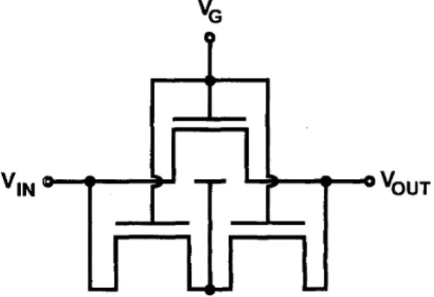
Fig. 2 shows the new asymmetrical dynamic threshold pass- transistor (ADTPT) circuit using NMOS devices. Different from the conventional dynamic threshold pass-transistor (DTPT) circuit, which includes two extra auxiliary transistors symmetrically as shown in Fig. 1, the ADTPT circuit as shown in Fig. 2 needs only one extra auxiliary transistor to control the body bias of the pass-transistor. In the conventional dynamic threshold pass-transistor (DTPT) circuit as shown in Fig. 1, the body of the main pass- transistor is connected to the source/drain node of the two auxiliary transistors with their gates tied to the gate of the main pass-transistor. In addition, the other sourceidrain nodes of these two auxiliary transistors are connected to the source and the drain of the main pass-transistor, respectively. Furthermore, the bodies of these auxiliary transistors are floating. In contrast, as shown in Fig. 2 , in the ADTPT circuit, the body of the main pass-transistor is connected to the sourceidrain node of the auxiliary transistor, whose gate is also tied to the gate of the main pass-transistor and its body is tied to the sourceidrain node of the main pass- transistor, instead of floating as in the conventional DTPT case.
(V,) is raised to VDD-VTN(VB=VnD), where V,(V,=V,,) is the threshold voltage of the auxiliary transistor biased with a body bias of V,=V,,. Compared to the conventional dynamic threshold pass-transistor (DTPT) circuit as shown in Fig. 1, the new ADTPT circuit has a faster speed owing to a higher body voltage provided by its auxiliary transistor
-
in the conventional dynamic threshold pass-transistor (DTPT) circuit, due to its two auxiliary transistor structure, the body bias of the main pass-transistor is half-way between the input V,, (=V,,) and the output VOUT, which rises from OV to VDD-VTN. In the new ADTPT circuit, owing to the single- auxiliary transistor structure, the body bias of the main pass- transistor is tied to a higher level VDD-V,,(V,=V,,). Therefore, the effective threshold voltage of the main pass- transistor of the new ADTPT circuit is much smaller as compared to the conventional case. As a result, a higher speed in passing the logic-1 signal from the input VI, to the output VoUT can be obtained.
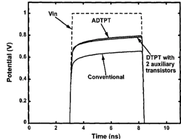
Fig. 3 shows the transient waveforms of (a) conventional pass-transistor circuit without an auxiliary transistor, (b) conventional dynamic threshold pass-transistor (DTPT) circuit with two auxiliary transistors, and (c) ADTPT circuit, during the pass-logic-1 operation, with 1V imposed at the gate and a voltage step from OV to 1V applied at the input of the main pass-transistor, based on MEDICI simulation results [ 8 ] . All transistors are SO1 NMOS devices with a channel length of 0.25-pm. The channel width of the main pass-transistor in the ADTPT circuit and the conventional
'IN
"G
'OUT
0.8-
AL
-
m 0.6 * B Q)2
0.4.
* 0.2.
2 auxiliary transistorsFigure 2. Asymmetrical dynamic threshold pass-transistor
(ADTPT) circuit.
The advantage of the new ADTPT circuit can be understood by considering its logic operation. When V, is high (VDD), both the pass-transistor and the auxiliary transistor are on. During the pass-logic-1 operation, the logic-1 level is propagated from the input V,, to the output V,",. When the input V,, increases from low to high, due to the function of the auxiliary transistor, the body of the main pass-transistor
0 2 4 6 8 10
Time (ns)
Figure 3. Transient waveforms of (a) conventional pass-
transistor circuit without an auxiliary transistor, (b) conventional dynamic threshold pass-transistor (DTPT) circuit with two auxiliary transistors, and (c) asymmetrical dynamic threshold pass-transistor (ADTPT) circuit, during the pass-logic-1 operation, with 1V imposed at the gate and a voltage step from OV to 1V applied at the input of the main transistor, based on MEDICI simulation results.
dynamic threshold pass-transistor (DTPT) circuit with two auxiliary transistors is 1-pm. The channel width of the conventional pass-transistor without the auxiliary device is 2-pm. The channel width of all auxiliary transistors is 0.3- pm. As shown in Fig. 3, due to the negative influence caused by the body effect, the output voltage V,,, of the conventional pass-transistor without an auxiliary transistor can only be raised to 0.66V in 5ns after the input VI, turns high to 1V. In contrast, the output of the conventional dynamic threshold pass-transistor (DTPT) circuit with two auxiliary transistors is raised to 0.75V at 511s. Among three, ADTPT circuit has the best performance - its output rises to 0.8V at 5ns, which is a 20% improvement as compared to the conventional pass-transistor without an auxiliary transistor. Although the two auxiliary transistors in the DTPT circuit provide an extra conduction path from the input to the output, the body voltage of its main pass- transistor cannot be enhanced effectively as compared to the ADTPT case, where the input voltage V,, affects the body voltage VB of the main pass-transistor and the auxiliary transistor simultaneously. Therefore, the threshold voltage of the main transistor in the ADTPT circuit can be reduced more effectively, which leads to a higher conduction capability of the main pass-transistor.
111
SO1 Complementary Pass-Transistor Logic
(CPL) with ADTPT
Complementary pass-transistor logic (CPL) circuit [7] is a
major technique for realizing digital VLSI logic circuits. A CPL circuit contains pass-transistors and inverters used as buffers at the end to recover the logic-] level. The new ADTPT technique is especially useful for implementing the CPL circuit. Fig. 4 and Fig. 5 show the AND/NAND logic circuits i m p l e m e n t e d b y the A D T P T technique and conventional DTPT technique with two auxiliary transistors,
Figure 4. ANDNAND CPL circuit implemented by ADTPT technique. BO- A B
1
-
-
B A-
B-
1
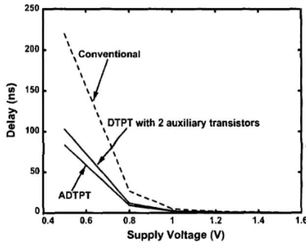
Figure 5. AND/NAND CPL circuit implemented by conventional DTPT technique with two auxiliary transistors. respectively. Fig. 6 shows fall time versus V,, of the three CPL circuits using (a) conventional pass-transistor circuit without an auxiliary transistor, (b) conventional DTPT technique with two auxiliary transistors, and (c) ADTPT technique. As shown in the figure, among three cases, the ADTPT one has the smallest fall time. In addition, at a smaller V,,, the advantages of the ADTPT technique are more noticeable
-
ADTPT technique is the most advantageous for use at a low supply voltage. Plus, the ADTPT technique is more concise as compared to the DTPT technique with two auxiliary transistors-
only one auxiliary transistor is required.\ \ \,Conventional
\\\\J
\ \I DTPT with 2 auxiliary transistors
K m r n
-.
ADTPT-.
1.2 1.4 1 4 0.6 0.8 6 Supply Voltage (V)Figure 6. Fall time versus V,, of the three CPL circuits using (a) conventional pass-transistor circuit without an auxiliary transistor, (b) conventional DTPT technique with two auxiliary transistors, and (c) ADTPT technique.
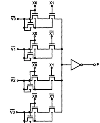
The compacmess of the ADTPT technique used for realizing low-voltage SO1 CPL is beyond our description so far. The strength in the conciseness of the ADTPT technique for low- voltage SO1 CPL can be demonstrated in a 4-to-1 multiplexer circuit implemented by SO1 CPL using ADTPT technique as shown in Fig. 7. Note that in Fig. 7, due to the complementary structure, only half of the circuit is drawn in the figure. As shown in the figure, instead of using an independent auxiliary transistor for each main pass-transistor in each row in the circuit, only one auxiliary transistor for
each row is sufficient.
v3
Figure
7.
A 4-to-1 multiplexer implemented by CPL using the ADTPT technique.IV
Conclusion
In this paper we report a novel low-voltage silicon-on- insulator (SOI) CMOS complementary pass-transistor logic (CPL) circuit using asymmetrical dynamic threshold pass- transistor (ADTPT) technique. Using the ADTPT technique to dynamically control the body bias of the pass-transistor via only one auxiliary transistor, the new SO1 CMOS complementary pass-transistor logic (CPL) circuit provides superior speed performance at a low supply voltage as
compared to the conventional pass-transistor logic circuits without the ADTPT technique as verified by the MEDICI simulation results. The ADTPT technique is especially effective for use in CPL circuits with serially-connected multiple inputs.
References
F. Assaderaghi, D. Sinitsky, S. A. Parke, J. Bokor, P. K. KO, and C. Hu, “Dynamic Threshold-Voltage MOSFET (DTMOS) for Ultra-Low Voltage VLSI”, IEEE Transactions on Electron Devices, Vol. 44, No. 3, pp. 414-422, March 1997.
C. T. Chuang, “Design Considerations of SO1 Digital CMOS VLSI”, Proceedings of IEEE International SO1 Conference, pp. 5-8, Oct. 1998.
I. Y. Chung, Y. J. Park, and H. S. Min, “A New SO1 Inverter Using Dynamic Threshold for Low-Power Applications”, IEEE Electron Device Letters, Vol. 18, No. 6, pp. 248-250, June 1997.
T. W. Houston, “A Novel Dynamic Vt Circuit Configuration”, Proceedings of IEEE International SO1 Conference, pp. 154-155, Oct. 1997.
J. B. Kuo and J. H. Lou, “Low-Voltage CMOS VLSI Circuits”, John Wiley: New York, ISBN 0471321052, 1999.
N. Lindert, T. Sugii, S. Tang, and C. Hu, “Dynamic Threshold Pass-Transistor Logic for Improved Delay at Lower Power Supply Voltages”, IEEE Journal of Solid- State Circuits, Vol. 34, No. 1 , pp. 85-89, Jan. 1999.
K. Yano, T. Yamanaka, T. Nishida, M. Saito, K. Shimohigashi, and A. Shimizu, “A 3.8-ns CMOS 16x16-b Multiplier Using Complementary Pass- Transistor Logic”, IEEE Journal of Solid-state Circuits, Vol. 25, No. 2, pp. 388-395, April 1990.
“MEDICI: Two-Dimensional Semiconductor Device Simulation,” Technology Modeling Associates, Inc., Palo Alto, CA, 1996.