EL.SEVIER Journal of Crystal Growth 150 (1995) 28-32
Formation and characterization
of GaAs/As
superlattice grown
by molecular beam epitaxy at low substrate temperature
T.M. Cheng a,*, C.Y. Chang a, J.H. Huang ba Institute of Electronics, National Chiao-Tung University, Hsinchu, Taiwan, ROC b Materials Science Center, National Tsing-Hua University, Hsinchu, Taiwan, ROC
Abstract
High-resolution X-ray diffractometer and transmission electron microscope (TEM) are used to characterize the redistribution of As precipitates in Si S-doped GaAs grown by molecular beam epitaxy at low substrate temperature (230°C). The superlattice satellite peaks are observed for samples annealed at 700-800°C for 10 min, which is attributed to the formation of a GaAs/As superlattice during the annealing period. The degree of As precipitates confined on the &doped planes is revealed on the intensity of satellite peaks in the X-ray rocking curves, as confirmed by the TEM observations. The lattice expansion and contraction of the annealed low-temperature epitaxial layers can be easily observed from the asymmetry of the satellite peaks.
1. Introduction
GaAs grown by molecular beam epitaxy (MBE) at low substrate temperature (LT) has recently received much attention, due to its unique elec- tronic and optical properties [l-6]. When grown at N 200°C the LT materials are very nonstoi- chiometric, containing about 1 at% excess As over those grown at conventional temperature [3] (N 600°C) and a high concentration of As-antisite defect [4]. The extremely short photoexcited car- rier lifetime (- 150 fs) [5] measured in LT GaAs makes it suitable for integrated subpicosecond
* Corresponding author.
optoelectronic switching. Upon post-growth an- nealing at 600°C the excess As precipitates into clusters [7] and the annealed LT GaAs exhibits very high resistivity which is desirable for many
device applications.
Warren et al. 181 proposed a simple model which assumed that the observed As precipitates were metallic and that the Schottky barrier height of As to GaAs held. Therefore, the control of precipitate density and position during annealing period has become an important issue in the point of device applications. Arsenic precipitates are found to form preferentially inside GaAs regions for LT GaAs/AlGaAs heterostructure [9] and inside InGaAs regions for LT GaAs/InGaAs heterostructure [lo]. The accumulation and de- pletion of As precipitates can also be achieved by 0022-0248/95/$09.50 0 1995 Elsevier Science B.V. All rights reserved
TM Cheng et al. /Journal of Crystal Growth 150 (1995) 28-32 29 incorporation of impurity [11,12]. Up to now, the
study of As precipitate distribution is performed by transmission electron microscope (TEM). In this work, the high-resolution double-crystal X-ray diffraction is used to characterize the redistribu- tion of As precipitates in the Si &doped LT GaAs. The superlattice satellite peaks in the rocking curve are observed for annealed samples. The evolution of satellite peak intensity can re- veal the degree of As precipitates confined on the Si S-doped planes, as confirmed by the TEM observations. The asymmetry of X-ray rocking curve intensity indicates the modulation in the lattice parameter of the annealed LT materials after annealing.
2. Experiment
The films used in this work were grown in a Varian GEN II MBE system using element solid source and tetramer As,. The growth rate was 1.0 pm/h for GaAs with an As,/Ga flux ratio (beam equivalent pressure) of 24. The substrate was nominally undoped semi-insulating (100) GaAs. Following native oxide desorption at 580°C a 0.3 pm GaAs buffer layer was deposited at 600°C to smooth the surface. The growth was then inter- rupted while maintaining the As, flux and the substrate temperature was ramped down to 230°C at which the Si S-doped LT-GaAs structure was grown. The low temperature structure consists of six Si &doped layers which are separated by 80 nm GaAs. The Si sheet density is 1.2 x 1013 cm-*. An identical structure but grown at 600°C is used as the control sample. After growth, the samples were cleaved into pieces and annealed for 10 min at the temperature range of 600-900°C in a form- ing gas ambient and with a GaAs proximity cap. The high-resolution X-ray diffraction measure- ments were carried out with a Philips DCD3 double-crystal diffractometer, equipped with a GaAs (004) as the first crystal. A JEM 2000FX electron microscope was used to examine the distribution of As precipitates. Cross-sectional samples parallel to Ill01 planes were prepared by mechanically thinning and Ar ion milling at low temperature for TEM observations.
3. Results and discussion 3.1. X-ray characterization
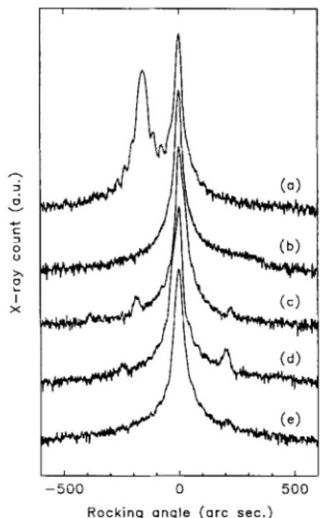
Figs. la-le show the (004) X-ray rocking curves for the Si &doped LT GaAs structure in the as-grown state and after annealing at 600, 700, 800, and 900°C for 10 min, respectively. For the as-grown sample (Fig. la), the perpendicular lat- tice mismatch in the LT GaAs layer is about 0.12% larger than the bulk GaAs substrate. The expansion of lattice constant of the as-grown LT GaAs is caused by the large concentration of As-antisite defects [4,13] incorporated during the film growth. The presence of well-defined inter- ference fringes in the X-ray rocking curve con- firms the high quality of the LT-epitaxial layers because the Pendellosung fringes occur only for high quality thin layers. After annealing at 600°C the lattice constant reduces and is very close to that of bulk GaAs, as shown in Fig. lb. The contraction of lattice constant after post-growth
-500 0 500
Rocking angle (arc sec.)
Fig. 1. (004) double-crystal X-ray rocking curves for Si S-doped LT GaAs under various annealing temperatures: (a) as-grown, and (b) 600, (c) 700, (d) 800, (e) 900°C annealed for 10 min.
30 T.M. Cheng et al. /Journal of Crystal Growth 150 (1995) 28-32
annealing can be explained by the removing of the As-antisite defects and formation of Ga va- cancies in the epitaxial layer during annealing period 1131. A striking feature in the rocking curves of both 700 and 800°C annealed samples is the presence of satellite peaks with asymmetric intensity around the main (004) GaAs peak, as shown respectively in Figs. lc) and Id). The satel- lite peaks intensity become very weak for sample annealed at a higher temperature of 900°C (Fig. le). To clarify that the satellite peaks are not due to the Si S-doped planes, X-ray analysis was also performed on the controlled wafer. The rocking curve shows only one peak due to Bragg reflec- tion from GaAs layer. The superlattice period A was averaged over the positions of the satellite peaks to be about 86 nm according to the equa- tion [141
(2 sin 8, - 2 sin Bs,)/A(Cu Ka,) = *n/A. The calculated period is close to the nominal undoped LT GaAs spacing of 80 nm between the Si a-doped layers.
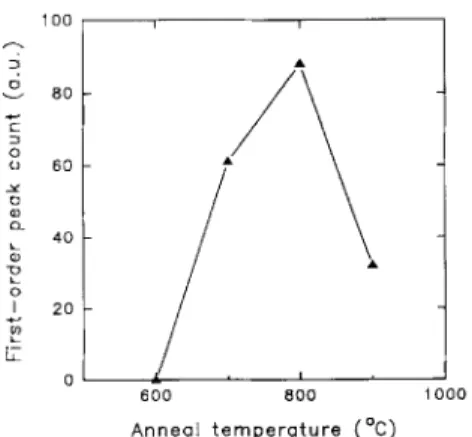
The dependence of the first-order satellite peak intensity on the annealing temperatures is shown in Fig. 2. The intensities first show an increase with annealing temperatures and gradu- ally reach the maximum value at 800°C. However, when annealed at higher temperatures, the inten- sities begin to decrease and finally become very weak.
T
-
O.00
Anneal temperature (“C)
Fig. 2. Dependence of the first order satellite peak intensity on the annealing temperatures for Si d-doped LT GaAs.
200 400 600 800 1000
Anneal temperature ( “C)
Fig. 3. Average lattice mismatch of the LT epitaxial layer with respect to the GaAs substrate.
In addition to the peak intensity variation as described above, slight shifts of satellite peak positions are observed for samples annealed at different temperatures, indicating the small varia- tion of the average lattice strain in the LT epi- layer with respect to the GaAs substrate. Fig. 3 summarizes the average lattice mismatch of the LT structures with respect to the GaAs substrate for different annealing temperatures. The lattice mismatch is calculated from the angular differ- ence between the GaAs substrate peak and the zeroth-order superlattice peak which is derived from the observed first order peaks. It shows a lattice contraction for 700°C annealing and a lattice expansion up to the order of 10d4 when annealed at 800 and 900°C. The lattice constant modulation of the epitaxial layers under different annealing temperatures can also be observed from the asymmetrical intensity of the superlattice peaks and GaAs substrate peak as observed in Fig. 1.
3.2. TEA4 characterization
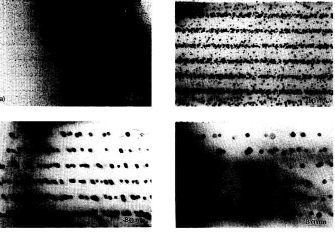
The evolution of X-ray rocking curves with annealing temperatures, as described above, can be explained consistently by the formation of GaAs/As superlattice due to the accumulation of As precipitates toward the Si &doped planes during the annealing period. The accumulation of precipitates may be due to the lower interfacial energy between As precipitate/Si doped GaAs,
TM. Cheng et al. /Journal of Crystal Growth 150 (1995) 28-32 31
compared to that between As precipitate/un- doped GaAs. Figs. 4a-4d are the bright-field TEM images of Si &doped LT GaAs annealed at 600, 700, 800, and 900°C respectively. For the 600°C annealed sample, As precipitates of 4 nm in diameter distribute nearly uniformly in the undoped LT-grown GaAs regions with a density of about 1.67 X 10¹⁷ cme3. Also seen is the slight accumulation of precipitates on the Si S-doped planes. For the 700°C annealed sample, the pre- cipitate coarsens to an average diameter of 16.7 nm on the doped planes. The precipitate density on the &doped planes increases with a reduction of the density inside the undoped regions. The periodic structure consisting of alternate GaAs and As precipitates permits a modulation of scat-
tering power [15] along the growth direction and consequently exhibits satellite peaks in the X-ray rocking curve. When annealing temperature in- creases to 800°C the As precipitates are totally confined on the Si &doped planes, which leaves the undoped regions free of precipitates. The well-defined precipitate/no precipitate region forms the superlattice-like structure and thus leads to the most pronounced satellite peaks in the rocking curve, as shown in Fig. Id and Fig. 2. When annealed at higher temperature of 900°C the precipitates further coarsen to about 23 nm. The spacing between the precipitates on the same S-doped plane is estimated to be 67.5 nm. The large spacing between precipitates reduces the periodicity along the growth direction to the ex-
32 TM. Cheng et al. /Journal of Crystal Growth 150 (1995) 28-32
tent that superlattice peaks are hardly observed in the X-ray rocking curve (Fig. le).
4. Conclusion
In this work, we demonstrate the high-resolu- tion X-ray analysis and TEM analysis of Si S- doped GaAs grown by molecular beam epitaxy at low substrate temperature. The satellite peaks in the X-ray rocking curves are observed for a sam- ple annealed at 700-800°C for 10 min, which is attributed to the formation of GaAs/As superlat- tice during annealing period. The intensity varia- tion of the satellite peaks reveals the confinement of As precipitates on the Si a-doped planes, as confirmed by the TEM observation. In contrast to TEM analysis, our results show that high-resolu- tion X-ray analysis can provide a nondestructive and easy way to characterize the diffusion of As precipitates in Si &doped LT GaAs. The GaAs/As superlattice will lead to a wide variety of device applications.
Acknowledgment
This work has been supported by the National Science Council, Republic of China, under con- tract NSC-82-0404-E009-239. References 111 121 131 141 El [61 [71 b31 [91 m illI KY
D.C. Look and D.C. Waiters, Phys. Rev. B 42 (1990) 3578.
D.D. Nolte, M.R. Melloch, J.M. Woodall and S.J. Ralph, Appl. Phys. Lett. 62 (1992) 1356.
F.W. Smith, A.R. Calawa, C.L. Chen, M.J. Manfra and L.J. Mahoney, IEEE Electron Device Lett. EDL-9 (1988) 77.
M. Kaminska, Z. Liliental-Weber, E.R. Weber, T. George and J.B. Kortright, Appl. Phys. Lett. 54 (1989) 1881. F.W. Smith, Mater. Res. Sot. Symp. Proc. 241 (1992) 3. Z. Liliental-Weber, W. Swider, K.M. Yu, J. Kortright, F.W. Smith and A.C. Calawa, Appl. Phys. Lett. 58 (1991) 2153.
M.R. Melloch, N. Otsuka, J.M. Woodall, A.C. Warten and J.L. Freeouf, Appl. Phys. Lett. 57 (1990) 1531. A.C. Warren, J.M. Woodall, J.L. Freeouf, D. Gis- chkowsky, D.T. McInturff, M.R. Melloch and N. Otsuka, Appl. Phys. Lett. 57 (1990) 1331.
K. Mahalingam, N. Otsuka, M.R. Melloch and J.M. Woodall, Appl. Phys. Lett. 60 (1992) 3253.
T.M. Cheng, A. Chin, C.Y. Chang, M.F. Huang, K.Y. Hsieh and J.H. Huang, Appl. Phys. L&t. 64 (1994) 1546. M.R. Melloch, N. Otsuka, K. Mahalingam, C.L. Chang, P.D. Kirchner, J.M. Woodall and A.C. Warren, Appl. Phys. Lett. 61 (1992) 177.
T.M. Cheng, C.Y. Chang, A. Chin, M.F. Huang and J.H. Hunag, Appl. Phys. Lett. 64 (1994) 2517.
[13] M. Fatemi, B. Tadayon, M.E. Twigg and H.B. Dietrich, Phys. Rev. B 48 (1993) 8911.
[14] J.M. Vandenberg, R.A. Hamm, A.T. Macrander, M.B. Panish and H. Temkin, Appl. Phys. Lett. 48 (1986) 1153. [15] R.M. Fleming, D.B. McWhan, A.C. Gossard, W. Wieg-