IEEE TRANSACTIONS ON ELECTRON DEVICES, VOL. 59, NO. 6, JUNE 2012 1807
Hydrogen Instability Induced by
Postannealing on Poly-Si TFTs
Chia-Chun Liao, Min-Chen Lin, and Tien-Sheng Chao
Abstract—This brief investigates hydrogen instability induced
by postannealing. Results show that using a SiN capping layer can prevent the release of hydrogen from a polycrystalline-silicon channel. However, removing this SiN capping layer allows the hydrogen release during postannealing, and the resulting device performance becomes comparable to that of the control sample. Hydrogen release reduces the immunity of PBTI and NBTI. Two possible mechanisms can explain the increased preexisting defects associated with hydrogen release, which affects the NBTI and PBTI.
Index Terms—Hydrogen release, NBTI, PBTI, plasma
dis-charge, postannealing.
I. INTRODUCTION
P
OLYCRYSTALLINE silicon (poly-Si) thin-film transis-tors (TFTs) have attracted attention recently, due to their potential applications in active-matrix liquid crystal displays and high-density vertical components [1]. Because the grain boundaries in poly-Si TFTs have a profound influence on device characteristics and degrade carrier transport, developing promising techniques to reduce the trap density is important. Previous research shows that hydrogen-plasma treatment and hydrogen-containing-nitride film deposition are promising ap-proaches for improving performance [2], because hydrogen radicals can effectively passivate the defects of intragrain, grain boundary, and the gate dielectric.In addition to using hydrogen plasma or hydrogen-containing nitride to passivate the traps deliberately, the hydrogen diffuses into the polysilicon during the fabrication process, in areas such as the buffered layer, the gate dielectric, and the hard mask of nanowires [3]. However, this hydrogen diffusion into the polysilicon easily suffers from subsequent thermal processes such as solid-phase crystallization, the deposition of gate di-electric, and the dopant activation, resulting in unavoidable hydrogen instability.
Postannealing decreases the benefits of using hydrogen rad-icals by plasma treatment to passivate these defects, indicating that there are limits to thermal cycling after the hydrogena-tion process. The effects of the postannealing temperature on
Manuscript received August 30, 2011; accepted March 13, 2012. Date of publication April 17, 2012; date of current version May 23, 2012. This work was supported by the National Science Council, Taiwan, under Contract NSC 97-2221-E-009-152-MY3. The review of this brief was arranged by Editor M. J. Kumar.
The authors are with the Department of Electrophysics, National Chiao Tung University, Hsinchu 300, Taiwan (e-mail: [email protected]).
Color versions of one or more of the figures in this paper are available online at http://ieeexplore.ieee.org.
Digital Object Identifier 10.1109/TED.2012.2191411
the poly-Si-TFT performance have also been studied experi-mentally [4]. However, the effects of the hydrogen instability induced by postannealing on the passivation of tail states, the passivation of deep states, and the additional defect generation in poly-Si TFTs must be clarified. To investigate the effects of hydrogen instability, it is necessary to eliminate the Si–H bonds completely by postannealing and avoid the issue of plasma damage.
In this brief, this study investigates the passivation efficiency of hydrogen using hydrogen-containing nitride. Although the issue of hydrogen has been thoroughly investigated for single-crystal MOSFETs [5], to our knowledge, this is the first time the issue of hydrogen release for poly-Si-TFT capped SiN has been demonstrated. These results indicate two types of defects: the original type of defect affected by passivation/depassivation and a second type generated by hydrogen release during subsequent annealing.
II. EXPERIMENTALPROCEDURE
An amorphous-silicon film measuring 500 Å thick was de-posited on thermally oxidized wafers at 500 ◦C by a low-pressure chemical vapor deposition (LPCVD). The wafers were annealed at 600 ◦C for 24 h to transform the amorphous film into poly-Si, and the poly-Si films were patterned into active islands. After removing the surface oxide, a 30-nm-thick tetraethyl orthosilicate (TEOS) oxide was deposited on the wafers. A 2000-Å-thick poly-Si was deposited and patterned to form the gate electrode, which also served as a mask for self-aligned implantation. The source/drain and gate regions were then implanted with phosphorous (15 keV at 5× 1015 cm−2) and activated at 600 ◦C for 24-h annealing in N2 ambient.
Then, a 10-nm-thick TEOS oxide was deposited. Furthermore, a 200-nm SiN was deposited by LPCVD at 780 ◦C for cou-pling hydrogen without plasma damage. During the deposition process, the hydrogen radicals diffused and passivated the defects in the channel. Under the same pressure, all samples received the same thermal budget by annealing in the nitrogen. The sample, denoted as SiN-removed, was capped by a 10-nm TEOS oxide and a 200-nm SiN layer originally. The capping SiN was then removed by a carefully selective wet-etching process. A 500-nm-thick TEOS oxide formed at 680 ◦C was adopted as the passivation layer as well as postannealing for all samples. After patterning the contact holes, aluminum was deposited by PVD and patterned as the probe pads to complete the TFT devices. Poly-Si TFTs of different channel widths from 10 to 0.8 μm and gate lengths from 10 to 1 μm were fabricated to analyze the passivation effects.
1808 IEEE TRANSACTIONS ON ELECTRON DEVICES, VOL. 59, NO. 6, JUNE 2012
Fig. 1. (a) Variation of threshold voltage as a function of channel width with
L = 10 μm for the control sample, the capped sample, and the
nitride-removed sample. (b) Variation of mobility as a function of channel width with
L = 10 μm for the control sample, the capped sample, and the
nitride-removed sample.
III. RESULTS ANDDISCUSSION
A. Hydrogen Instability Induced by Postannealing
Fig. 1(a) and (b) demonstrates the threshold voltage and mobility as a function of width. The threshold voltage (Vth)
is defined as the gate voltage required to achieve a normal-ized drain current of ID= (W/L)× 100 nA at VDS= 0.1 V.
The threshold voltage of the control sample decreases as the channel widths fall from 10 down to 0.8 μm, since the gate control is further increased with decreasing channel width due to corner-portion domination [1]. The field-effect mobility
μFE is extracted from the maximum transconductance. It is
noted that the passivation effect by PECVD SiN passivation layer or plasma discharge exhibits strong width dependence, since the portion of the poly-Si channel without passivation by radicals is minimized as the channel width is scaled down [2]. The improvements in threshold voltage and mobility by capping LPCVD SiN are significant for all width dimensions, implying that the LPCVD SiN passivation layer exhibits higher passivation efficiency.
The SiN-removed sample reveals threshold voltage and mo-bility characteristics comparable to those of the control sample. It is noted that the deep states, which originate from the dangling bonds in the grain boundaries, influence the threshold voltage and the subthreshold swing. However, tail states, which originate from the intragrain defects, affect the field-effect mobility and the minimum leakage current [2]. This implies that postannealing breaks both the passivation of the dangling bonds and the intragrain defects by hydrogen, which in turn decreases the improvement in threshold voltage and mobility. By the same token, the comparison shows that the SiN capping layers can strengthen the immunity against the postannealing, due to the suppression of hydrogen outgassing during postannealing.
Fig. 2 shows the drain-current-versus-drain-voltage (ID–VD)
characteristics of all n-channel poly-Si TFTs. The SiN-200-nm sample exhibits a significantly better performance than the control sample due to a reduction in the tail state density. The SiN-removed sample exhibits a performance comparable to that
Fig. 2. Output characteristics (the ID–VD curve) of n-channel TFTs with W/L = 10 μm/10 μm for the control sample, the nitride-capped sample, and
the nitride-removed sample.
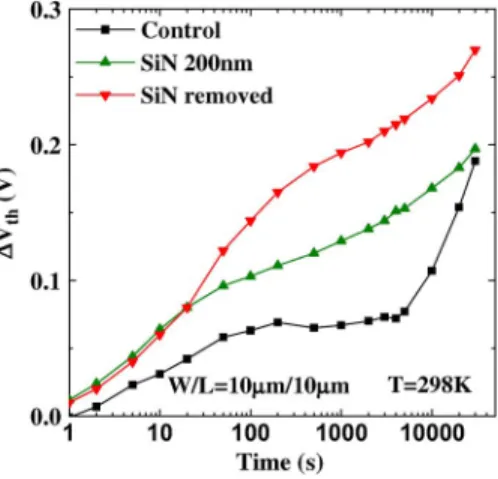
Fig. 3. Threshold-voltage shift as a function of stress time for the con-trol sample, the nitride-capped sample, and the nitride-removed sample with
W/L = 10 μm/10 μm under positive gate bias stress as VGS= 19 V.
of the control sample, indicating that the Si–H bonds, which affect the electrical properties, break completely.
Fig. 3 shows the time dependence of threshold-voltage shift ΔVth of the n-channel TFTs after the PBTI stress with VG=
19 V and VD= Vs= 0 V for 30 000 s at T = 25 ◦C. BTI
degradation was evaluated by the conventional method in which
ID–VGcurves are measured during stress interruption. It can be
seen that the increase in the ΔVthof the SiN-removed sample
is higher than that of the TEOS-10-nm and control samples, implying a raised defect density.
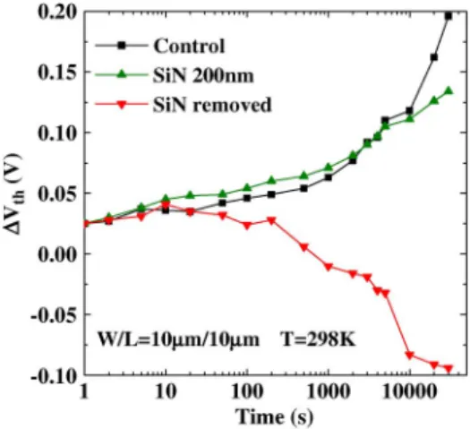
Fig. 4 shows the time dependence of the threshold-voltage shift ΔVth of the n-channel TFTs after the NBTI stress with VG=−19 V and VD= Vs= 0 V for 30 000 s at T = 25◦C.
The control sample and SiN-200-nm sample exhibit an increas-ing threshold voltage after NBTI stressincreas-ing, but the SiN-removed sample exhibits a decreasing threshold voltage. Furthermore, the insignificant degradation of the subthreshold swing indi-cates insignificant negatively charged ΔQit (not shown here).
Thus, the different dominant charge trappings are responsible for the different immunities of the NBTI, implying differ-ent oxide quality and channel conditions. As a result, the control sample and the SiN-removed sample exhibit different
LIAO et al.: HYDROGEN INSTABILITY INDUCED BY POSTANNEALING ON Poly-Si TFTs 1809
Fig. 4. Threshold-voltage shift as a function of stress time for the con-trol sample, the nitride-capped sample, and the nitride-removed sample with
W/L = 10 μm/10 μm under negative gate bias stress as VGS=−19 V.
immunities to NBTI stressing, although their original perfor-mances are comparable. It is known from the literature that the interface between the poly-Si channel and gate oxide exhibits better quality than the interface between the poly-Si gate and gate oxide [6]. The nonideal interface between the poly-Si gate and gate oxide results in the significant electron injection from the poly-Si gate under negative bias stressing. On the other hand, the hydrogen release degrades the interface between the poly-Si channel and gate oxide, and the hole injection from the poly-Si channel becomes higher than the electron injection from the poly-Si gate, as a result.
Based on our results, there are two possible mechanisms for the increase in preexisting defects in the SiN-removed sample. The first mechanism is the hydrogen or hydroxide group, which does not affect the original performance as strongly as the control sample, inducing traps, preexistent to the stress or created during the stress in the gate oxide [7]. The second possible cause is the out diffusion of hydrogen released from the intragrain or grain boundary, since such hydrogen migra-tion may generate defects, such as platelets, H2 defects, and
vacancies in the poly-Si channel [8].
IV. CONCLUSION
This brief has investigated the effects of hydrogen instability induced by postannealing on device performance and relia-bility. For the SiN-removed sample, postannealing decreases the improvements of defect passivation. Devices with a SiN capping layer can suppress the outgassing of hydrogen while retaining the improvement in mobility and threshold voltage.
Hydrogen release reduces the immunities of PBTI and NBTI. Samples experiencing hydrogen release have exhibited the worst degradation of PBTI. For NBTI concerns, the dominant degradation mechanism of the threshold voltage of the SiN-removed sample has been the hole trapping rather than the elec-tron trapping, which has been the mechanism that affects both the control sample and the capped SiN sample. Two possible mechanisms can explain the increased preexisting defects that affect the NBTI and PBTI.
ACKNOWLEDGMENT
The authors would like to thank the National Nano Device Laboratories and the Nano Facility Center, National Chiao Tung University, for the process.
REFERENCES
[1] M. C. Tsai, T. C. Liao, I. C. Lee, and H. C. Cheng, “Passivation-induced subthreshold kink effect of ultrathin-oxide low-temperature polycrystalline silicon thin film transistors,” IEEE Electron Device Lett., vol. 32, no. 7, pp. 904–906, Jul. 2011.
[2] C. C. Liao, M. C. Lin, T. Y. Chiang, and T. S. Chao, “Effects of channel width and nitride passivation layer on electrical characteristics of polysil-icon thin film transistors,” IEEE Trans. Electron Device, vol. 58, no. 11, pp. 3812–3819, Nov. 2011.
[3] C. W. Luo, H. C. Lin, K. H. Lee, W. C. Chen, H. H. Hsu, and T. Y. Huang, “Impacts of nanocrystal location on the operation of trap-layer-engineered poly-Si nanowired gate-all-around SONOS memory devices,” IEEE Trans.
Electron Devices, vol. 58, no. 7, pp. 1879–1885, Jul. 2011.
[4] F. S. Wang, M. J. Tsai, and H. C. Cheng, “The effects of NH3 plasma
passivation on polysilicon thin-film transistors,” IEEE Electron Device
Lett., vol. 16, no. 11, pp. 503–505, Nov. 1995.
[5] Z. F. Zhang, H. K. Sii, R. Degraeve, and G. Groeseneken, “Mechanism for the generation of interface state precursors,” J. Appl. Phys., vol. 87, no. 6, pp. 2967–2977, Mar. 2000.
[6] T. F. Lei, J. Y. Cheng, S. Y. Shiau, T. S. Chao, and C. S. Lai, “Characteri-zation of polysilicon oxides thermally grown and deposited on the polished polysilicon films,” IEEE Trans. Electron Devices, vol. 45, no. 4, pp. 912– 917, Apr. 1998.
[7] V. Huard, M. Denais, F. Perrier, N. Revil, C. Parthasarathy, A. Bravaix, and E. Vincent, “A thorough investigation of MOSFETs NBTI degradation,”
Microelectron. Reliab., vol. 45, no. 1, pp. 83–98, Jan. 2005.
[8] F. A. Reboredo, M. Ferconi, and S. T. Pantelides, “Theory of the nucleation, growth, and structure of hydrogen-induced extended defects in silicon,”
Phys. Rev. Lett., vol. 82, no. 24, pp. 4870–4873, Jun. 1999.
Chia-Chun Liao was born in Taoyuan, Taiwan, in
1980. He received the B.S. degree in electrophysics from National Chiao Tung University, Hsinchu, Taiwan, in 2007. He is currently working toward the Ph.D. degree in the Department of Electrophysics, National Chiao Tung University.
His research interests include strain technique, PEALD for metal gate/high-k application, and non-volatile flash memories.
Min-Chen Lin was born in Tainan, Taiwan, in 1986.
She received the B.S. degree in physics from the Na-tional Cheng Kung University, Tainan, in 2008 and the M.S. degree from the Institute and Department of Electrophysics, National Chiao Tung University, Hsinchu, Taiwan, in 2011.
She is currently with the Department of Elec-trophysics, National Chiao Tung University. Her research interests are the fabrication and charac-terization of nonvolatile flash memory and high-k dielectrics.
Tien-Sheng Chao was born in Penghu, Taiwan, in
1963. He received the Ph.D. degree in electronics engineering from National Chiao Tung University, Hsinchu, Taiwan, in 1992.
In July 1992, he joined the National Nano De-vice Laboratories as an Associate Researcher, where he became a Researcher in 1996. He was engaged in developing thin-dielectrics preparations, clean-ing processes, and CMOS device fabrication. Then, since 2001, he has been with the Department of Elec-trophysics, National Chiao Tung University, where he became a Professor in 2002.