IEEE PHOTONICS TECHNOLOGY LETTERS, VOL. 20, NO. 8, APRIL 15, 2008 659
High-Brightness InGaN–GaN Flip-Chip
Light-Emitting Diodes With Triple-Light
Scattering Layers
Chia-En Lee, Yea-Chen Lee, Hao-Chung Kuo, Senior Member, IEEE, Tien-Chang Lu, Associate Member, IEEE,
and Shing-Chung Wang, Life Member, IEEE
Abstract—The flip-chip light-emitting diodes (FC-LEDs) with
triple-light scattering layers were investigated comprising a top surface sapphire textured layer, an interface patterned sap-phire layer, and a bottom naturally textured p-GaN layer. Such triple-textured layers are useful for light extraction efficiency enhancement. The light output power of FC-LEDs was increased 60% (at 350-mA current injection) compared to that of conven-tional FC-LEDs by implementing the triple-light scattering layers.
Index Terms—Flip-chip light-emitting diodes (FC-LEDs),
natu-rally textured p-GaN layer, patterned sapphire, sapphire textured layer, triple-light scattering layers.
I. INTRODUCTION
W
IDE BANDGAP light-emitting diodes (LEDs) that are III–nitride, ranging from ultraviolet to the short-wavelength part of the visible spectrum have been intensely developed in the past ten years [1]. Recently, as the brightness of GaN-based LEDs has increased, applications such as traffic signals, backlight for cell phones, and LCD-TV have become possible [2]. However, as for the replacement of the conventional fluorescent lighting source with solid-state lighting, it still needs a great effort for improving the light extraction efficiency. The conventional LEDs are inherently inefficient because photons are generated through a sponta-neous-emission process and emitted in all directions. A large fraction of light emitted downward toward the substrate does not contribute to usable light output. In addition, there is an inherent problem associated with conventional nitride LEDs, i.e., the poor thermal conductivity of the sapphire substrate. It has been shown that the flip-chip technique is an effective way to further enhance light extraction and heat dissipation [3]. The flip-chip light-emitting diodes (FC-LEDs) configuration has high extraction efficiency compared to that of conventional LEDs due to the lower refraction index contrast between sap-phire substrate ( ) and air ( ). This leads a critical angle of light output to become larger and let total internalManuscript received November 23, 2007; revised January 6, 2008. This work was supported in part by the MOE ATU Program, and in part by the National Science Council of the Republic of China (R.O.C.) in Taiwan under Contract NSC95-2221-E009-235-MY3 and Contract NSC96-2628-E009-017-MY3.
The authors are with the Institute of Electro-Optical Engineering, National Chiao Tung University, Hsinchu 300, Taiwan, R.O.C. (e-mail: hckuo@faculty. nctu.edu.tw).
Color versions of one or more of the figures in this letter are available online at http://ieeexplore.ieee.org.
Digital Object Identifier 10.1109/LPT.2008.919509
reflection reduce. Furthermore, metal contact including n- and p- metal of FC-LEDs would not baffle light output. However, FC-LEDs still have a total internal reflection effect between the GaN–air, GaN–sapphire, and sapphire–air interfaces, reducing the extraction efficiency of FC-LEDs.
Previously, there has been more and more intensive research in the enhancement of light extraction efficiency. The surface texturing effect on light extraction efficiency enhancement was discussed in many papers [3], [4], [7]. Tsai et al. reported the high efficiency GaN-based LEDs with naturally textured surface grown by metal–organic chemical vapor deposition (MOCVD) [3], [4]. Huang et al. reported the enhancement of light extraction efficiency by nano-roughened p-GaN sur-face [5]. Horng et al. reported the indium–tin–oxide (ITO) textured window layers using natural lithography for light extraction improvement [6]. Han et al. reported the light ex-traction improvement of FC-LEDs by texturing the bottom side surface of the sapphire substrate [7]. Besides, epi-growth on pattern sapphire substrate (PSS) can reduce dislocation density in the epitaxial layers and also enhance light scattering at GaN-sapphire interface [8]–[10]. Feng et al. reported the luminescence enhancement from GaN-based blue LEDs grown on grooved sapphire substrates [8]. Wuu et al. reported the near-ultraviolet LEDs grown on PSS [9]. Lee et al. reported the output power enhancement of GaN-based LEDs grown on wet-etched PSS [10]. All these methods have one thing in common, which is that photons generated within the LEDs can experience multiple opportunities to find the escape cone. As a result, the light extraction efficiency and the LED output intensity could both be enhanced significantly. In this letter, nitride-based FC-LEDs with triple-light scattering layers were fabricated by a combination of epi-growth naturally textured surface, epi-growth on PSS, and micro-pillar arrays sapphire surface techniques. The detail of device fabrications and char-acteristics will be discussed.
II. EXPERIMENT
The GaN LED wafers used in this study were grown by MOCVD onto c-face (0001) 2-in diameter PSS.
Fabrication of PSS was illustrated as follows: the Ni films with bump-array patterns of 3- m diameter and 3- m spacing were deposited onto the sapphire substrate by e-beam evaporator and defined by standard photolithography to serve as the dry-etching hard mask. The sapphire substrate was then dry etched using an inductively coupled plasma
660 IEEE PHOTONICS TECHNOLOGY LETTERS, VOL. 20, NO. 8, APRIL 15, 2008
Fig. 1. Schematic drawing of the FC-LEDs with triple-light scattering layers.
(ICP) etcher with an etching depth of 1 m. In this study, a GaN-LED structure comprised a 1.5 m-thick undoped GaN layer, a 2.5- m-thick highly conductive n-type GaN layer, a 0.2- m-thick InGaN–GaN multiple quantum-well, a 0.2- m-thick p-type GaN layer, and InGaN–GaN short-period super-lattice tunneling contact layers for ITO ohmic contact. Top-emitting LEDs with a size of 1000 m 1000 m were fabricated using standard photolithography and ICP etcher for current isolation purposes. The p-GaN and active layers were partially etched by an ICP etcher to expose an n-GaN layer for electrode formation. An ITO film (250 nm) was deposited on the p-GaN layer as the transparent conductive layer.
The samples were then annealed at 500 C for 10 min in air. The Cr–Pt–Au (50 nm/50 nm/2500 nm) metals were de-posited for the p- and n-contact pads. After completing the con-ventional face-up LED structure, the Ni (500 nm) metal with bump-array patterns of 3- m diameter and 3- m spacing was deposited onto the bottom side of sapphire substrate as the hard mask. The sample was then subjected to the ICP process using – (10 sccm/30 sccm) plasma with an ICP power of 850 W and RF power of 400 W to form the micro-pillar ar-rays surface for light extraction purposes. The processed LED wafer was then subjected to the laser scribe and broken into 1000 1000 m chips. Finally, the LED chips were flip-chip bonded on a SiO –Al (80 nm/200 nm) coated silicon submount using Panasonic ultrasonic flip-chip bonder for electrical and optical measurement. A schematic drawing of the GaN FC-LED with triple-light scattering layers including a top pineapple-like pillar arrays surface layer, interface pattern sapphire layer, and bottom naturally textured p-GaN layer was shown in Fig. 1.
III. RESULTS ANDDISCUSSION
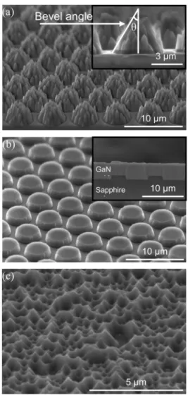
The surface morphologies of triple-light scattering layers were examined by scanning electron micrographs, as shown in Fig. 2(a)–(c). Fig. 2(a) shows the top sapphire surface with 5.5- m periodic distance and 3.2- m depth of pillar-arrays structure. Such a pineapple-like pillar surface could be ascribed to the nonuniform Ni hard mask and various etching rate in the center and rim areas of etch pillar which result in a partial over etching and the uneven pillar surface. Fig. 2(b) shows the PSS before and after epi-growth [inserted figure]. In this study, the patterns with 3- m diameter, 3- m spacing, and 1- m etching depth were formed on the sapphire substrate for epi-growth. According to the inserted figure, the PSS can be buried com-pletely by a GaN epitaxial layer without the appearance of a void. Shown in Fig. 2(c) is the naturally textured surface grown by MOCVD.
Fig. 2. Scanning electron microscope of surface morphology of (a) top surface sapphire textured layer, (b) interface pattern sapphire layer, and (c) bottom nat-urally textured p-GaN layer.
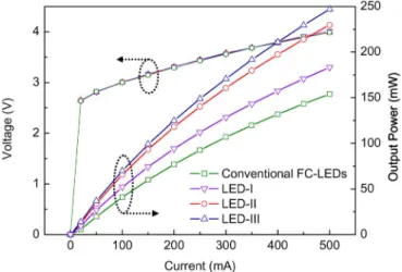
In this study, four types of FC-LEDs were fabricated for comparison: conventional FC-LEDs, FC-LEDs with a bottom side naturally textured p-GaN surface [LED-I], FC-LEDs with a bottom side naturally textured p-GaN surface and interface PSS layer [LED-II], and FC-LEDs with triple-light scattering layers [LED-III]. The corresponding current–voltage ( – ) and output power–current ( – ) characteristics of these four types FC-LEDs were shown in Fig. 3. It was found that the – curves were almost identical for these devices. The for-ward voltage (at 350 mA) was all about 3.55 V for these four devices. The similarity of electrical property indicates that the implementing of triple-light scattering layers would not result in any degradation in the electrical properties of nitride-based FC-LEDs. According to the – curves, it could be seen that output power of LED-I, -II, and -III were all larger than that of conventional FC-LEDs. By adopting the naturally textured p-GaN layer, the TIR effect can be reduced and the light escape probability can be increased at the GaN–air interface resulting in the higher output power of LED-I. Furthermore, the output power can be further enhanced by epi-growth on PSS. The interface PSS not only reduces the dislocation but increases the light scattering from GaN to sapphire substrate. Finally,
LEE et al.: HIGH-BRIGHTNESS InGaN–GaN FC-LEDs WITH TRIPLE-LIGHT SCATTERING LAYERS 661
Fig. 3. Corresponding I–V and L–I characteristics of the four types of FC-LEDs.
by a combination of epi-growth naturally textured surface, epi-growth on PSS, and micro-pillar array sapphire surface techniques, it is found that the light output power of LED-III could be significantly raised from 119 to 191 mW under 350-mA current injections compared to that of conventional FC-LEDs. This result can be attributed to the implementation of triple-light scattering layers. The internal quantum effi-ciency and external quantum effieffi-ciency could be improved by epi-growth on the PSS. Beside, a top pineapple-like textured sapphire surface and bottom naturally textured p-GaN surface can efficiently reduce the totally internal reflection effect and enhance the light extraction from sapphire to air and GaN to air, respectively. The LED-III offers a significant advantage over conventional FC-LEDs by facilitating light emission from the top pineapple-like pillar array surface and bottom naturally textured p-GaN surface. By these arts, it is noted that the bare FC-ELDs with triple-light scattering layers (without an epoxy lens encapsulated) present 60% output power enhancement at 350-mA current injection compared to that of conventional FC-LEDs. To further investigate the influence of triple-light scattering layers on light–output performance of an LED chip, intensity distribution measurements were performed on LED-III and conventional FC-LEDs. Fig. 4 shows the photos of the devices under 20-mA current injections. Each light output intensity distributions is also shown in the same figure. It was obviously observed that the EL intensities of LED-III clearly exceeded those of conventional FC-LED under the same injec-tion current at the top surface area. Such an enhancement could be attributed to the adopting of triple-light scattering layers that photos could have a larger probability to emitted from the device and, thus, achieve even brighter LEDs.
Fig. 4. Intensity distribution of (a) LED-III and (b) conventional FC-LED with a 20-mA injection current.
IV. SUMMARY
The FC-LEDs with triple-light scattering layers were inves-tigated. The formation of the FC-LEDs’ structure increased the light output power up to 60%. The novel FC-LEDs’ structure could not only reduce the TIR effect but efficiently facilitate light emission from the top pineapple-like pillar arrays surface and bottom naturally textured p-GaN surface.
REFERENCES
[1] E. F. Schubert and J. K. Kim, “Solid-state light sources getting smart,”
Science, vol. 308, pp. 1274–1278, 2005.
[2] A. Zukauskas, M. S. Shur, and R. Gaska, Introduction to Solid-State
Lighting. New York: Wiley.
[3] C. M. Tsai, J. K. Sheu, W. C. Lai, Y. P. Hsu, P. T. Wang, C. T. Kuo, C. W. Kuo, S. J. Chang, and Y. K. Su, “Enhanced output power in GaN-based LEDs with naturally textured surface grown by MOCVD,”
IEEE Electron. Device Lett., vol. 26, no. 7, pp. 464–466, Jul. 2005.
[4] C. M. Tsai, J. K. Sheu, P. T. Wang, W. C. Lai, S. C. Shei, S. J. Chang, C. H. Kuo, C. W. Kuo, and Y. K. Su, “High efficiency and improved ESD characteristics of GaN-based LEDs with naturally textured sur-face grown by MOCVD,” IEEE Photon. Technol. Lett., vol. 18, no. 11, pp. 1213–1215, Jun. 1, 2006.
[5] H.-W. Huang, C. C. Kao, J. T. Chu, H. C. Kuo, S. C. Wang, and C. C. Yu, “Improvement of InGaN–GaN light-emitting diode performance with a nano-roughened p-GaN surface,” IEEE Photon. Technol. Lett., vol. 17, no. 5, pp. 983–985, May 2005.
[6] R. H. Horng, C. C. Yang, J. Y. Wu, S. H. Huang, C. E. Lee, and D. S. Wuu, “GaN-based light-emitting diodes with indium tin oxide tex-turing window layers using natural lithography,” Appl. Phys. Lett., vol. 86, pp. 221101-1–221101-3, 2005.
[7] D.-S. Han, J.-Y. Kim, S.-I. Na, S.-H. Kim, K.-D. Lee, B. Kim, and S.-J. Park, “Improvement of light extraction efficiency of flip-chip light-emitting diode by texturing the bottom side surface of sapphire sub-strate,” IEEE Photon. Technol. Lett., vol. 18, no. 13, pp. 1406–1408, Jul. 1, 2006.
[8] Z. H. Feng and K. M. Lau, “Enhanced luminescence from GaN-based blue LEDs grown on grooved sapphire substrates,” IEEE Photon.
Technol. Lett., vol. 17, no. 9, pp. 1812–1814, Sep. 2005.
[9] D. S. Wuu, W. K. Wang, W. C. Shih, R. H. Horng, C. E. Lee, W. Y. Lin, and J. S. Fang, “Enhanced output power of near-ultraviolet InGaN–GaN LEDs grown on patterned sapphire substrates,” IEEE
Photon. Technol. Lett., vol. 17, no. 2, pp. 288–290, Jan. 15, 2006.
[10] Y. J. Lee, J. M. Hwang, T. C. Hsu, M. H. Hsieh, M. J. Jou, B. J. Lee, T. C. Lu, H. C. Kuo, and S. C. Wang, “Enhancing the output power of GaN-based LEDs grown on wet-etched patterned sapphire substrates,”
IEEE Photon. Technol. Lett., vol. 18, no. 10, pp. 1152–1154, May 15,