1148 IEEE ELECTRON DEVICE LETTERS, VOL. 29, NO. 10, OCTOBER 2008
High-Program/Erase-Speed SONOS With
In Situ Silicon Nanocrystals
Tsung-Yu Chiang, Tien-Sheng Chao, Yi-Hong Wu, and Wen-Luh Yang
Abstract—In this letter, for the first time, we have successfully
fabricated silicon–oxide–nitride–oxide–silicon (SONOS) devices with embedded silicon nanocrystals (Si-NCs) in silicon nitride using in situ method. This process is simple and compatible to modern IC processes. Different Si-NCs deposition times by in situ method were investigated at first. SONOS devices with embedded Si-NCs in silicon nitride exhibit excellent characteristics in terms of larger memory windows (> 5.5 V), lower operation voltage, high P/E speed, and longer retention time (> 108s for 13% charge loss).
Index Terms—Memory window, nonvolatile memory, retention
time, silicon nanocrystals (Si-NC).
I. INTRODUCTION
A
CCORDING to the International Technology Roadmap for Semiconductors (ITRS), one of the challenges for floating-gate memories is the scaling of the tunneling oxide [1]. Metal–oxide–semiconductor (MOS) memories with embedded silicon nanocrystal (Si-NC) and silicon–oxide– nitride–oxide–silicon (SONOS) nonvolatile memories have re-cently obtained a lot of attention due to their feasibility to overcome the limit of conventional polycrystalline-silicon-based floating-gate memories [2]–[4]. SONOS memories can offer several advantages over the traditional floating-gate Flash memories: simple process, high density, elimination of the drain-induced turn-on effect, multibit operation, no floating-gate coupling effect, and excellent immunity to stress-induced leakage current [5]–[8]. Si-NC memories have attracted a great interest to improve the problem of retention and endurance [9]–[15]. The SiN/Si-NCs/SiN trapping layers are used [13]; however, the deposition is not in situ. Hybrid Si-NCs/SiN trapping layers are reported [14], in which the Si-NCs are not embedded in nitride. In [15], SiN/Si-NCs/SiN trapping layers are investigated, but Si-NCs are realized by low-energy SiH4plasma-immersion ion implantation. In this letter, for the first time, SONOS memories with embedded Si-NCs formed by
in situ deposition in nitride is proposed. This in situ deposition
Manuscript received March 7, 2008; revised July 14, 2008. First published September 9, 2008; current version published September 24, 2008. This work was supported by the National Science Council, Taiwan, R.O.C., under Con-tract NSC-95-2221-E-009-272. The review of this letter was arranged by Editor K. De Meyer.
T.-Y. Chiang and T.-S. Chao are with the Department of Electrophysics, National Chiao Tung University, Hsinchu 300, Taiwan, R.O.C. (e-mail: [email protected]).
Y.-H. Wu and W.-L. Yang are with the Department of Electronic Engineer-ing, Feng Chia University, Taichung 407, Taiwan, R.O.C.
Color versions of one or more of the figures in this letter are available online at http://ieeexplore.ieee.org.
Digital Object Identifier 10.1109/LED.2008.2002944
Fig. 1. (a) Cross-sectional scheme of Si-NCs SONOS memory structure with the nitride film embedded with the Si-NCs. (b) Gas flow of in situ deposition of Si-NCs in nitride.
method exhibits a simple fabrication process and is compatible to the modern complementary MOS technologies. At first, we focus on the comparison of performance and reliability for the Si-NCs deposition for different times for 10, 30, 60, and 90 s. SONOS memories with Si-NCs show improved performance in terms of larger memory windows, lower operation voltage, higher P/E speed, and longer retention time than without one.
II. EXPERIMENTALPROCEDURE
Fig. 1(a) shows the device’s structure. P-type silicon (100) wafers were used. After local-oxidation-of-silicon, or LOCOS, isolation step, a tunneling oxide was first thermally grown in N2O (2.5 nm). The in situ step includes three phases. Fig. 1(b)
shows the change of gas flow of SiH2Cl2and NH3during these
three phases of deposition step. At the first phase, a 3-nm-thick silicon-nitride film was deposited in a low-pressure chemical-vapor-deposition (LPCVD) system using SiH2Cl2 (130 sccm)
and NH3(30 sccm) at 780◦C. In the second phase, in the same
tube, NH3was turned off. Wafers were then in situ deposited a
thin Si-NCs grown only by using SiH2Cl2(10 sccm, pressure
∼300 mtorr, at 780◦C) for 10, 30, 60, and 90 s, respectively.
CHIANG et al.: HIGH-PROGRAM/ERASE-SPEED SONOS WITH IN SITU SILICON NANOCRYSTALS 1149
Fig. 2. Program and erase speed of SONOS with different growth time of Si-NCs.
To sandwich Si-NCs in nitride, a final top 4-nm silicon nitride was deposited in the same tube by turning on the NH3gas again
at the third phase. These Si-NCs can be easily in situ embedded into nitride by the alternative switching of NH3 gas. All these
three steps were executed in the same tube and at the same temperature. Hence, wafers do not need to change tube during fabrication. The mean size of Si-NCs and aerial density turned out to be 7–10 nm and 7−9 × 1011 cm−2, respectively. We found that a longer deposition time results in a larger Si-NCs size. A blocking oxide about 20-nm was then deposited using high-density plasma CVD. A 200-nm-thick poly-Si film was deposited as the control gate. Standard MOSFET fabricating steps were followed to complete final devices.
III. RESULTS ANDDISCUSSION
Fig. 2 shows the program and erase speed characteristic for all samples. We programmed and erased each sample by using channel electron injection and band-to-band hot-hole injection for NOR-architecture application, respectively. Programming was set at VG = VD= 6 V, while erasing was set at VG=−8 V and VD= 8 V. The zero point of Vt shift in the figure is the initial state before programming in program speed and programmed before erasing in erase speed. The shift of threshold voltage (memory window) of SONOS with Si-NCs deposition for 10, 30, 60, and 90 s are 4.4, 6.1, 5.5, and 5.7 V, respectively. We found that the optimum time of deposition is 30 s in P/E speed characteristic. Since a typical sense amplifier can be designed to detect shift of memory window as low as 0.5 V [16]. Therefore, the resultant memory window about 5.5 V is large enough for multilevel operation. From these curves, we found that a relatively fast programming (t = 10 μs)
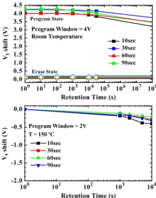
Fig. 3. Data-retention characteristic of different samples after programming ΔVt= 4 V at T = 25◦C and programming ΔVt= 2 V at T = 150◦C.
Fig. 4. Endurance characteristics obtained for the SONOS with in situ Si-NCs memory device with 30-s deposition time.
and erasing (t = 100 μs) time can be achieved for a 2.3-V shift of threshold voltage. This significant improvement of devices with in situ Si-NCs can be attributed to newly created trapping site in Si-NCs, or at the interface of silicon nitride and Si-NCs. Therefore, a relatively large resultant memory window and faster P/E speed can be obtained for SONOS with embedded Si-NCs. It is noted that SONOS with only 10-s deposition time has less performance improvement which could be due to the smallest Si-NCs size and density among these samples.
The data-retention characteristics of the different Si-NCs memories at room temperature (T = 25◦C) and high temper-ature (T = 150◦C) are shown in Fig. 3. At room temperature, the charge loss was below 13%, as extrapolated to 108s. When operated at 150◦C, it exhibits only 10% charge loss for 104s. With Si-NCs, deep charge-trapping level can be created at the interface of Si-NCs and nitride, resulting in an improved data
1150 IEEE ELECTRON DEVICE LETTERS, VOL. 29, NO. 10, OCTOBER 2008
TABLE I
COMPARISONS OFP/E VOLTAGE, P/E SPEED, CHARGELOSS ATROOMTEMPERATURE(T = 25◦C),ANDHIGHTEMPERATURE(T = 150◦C)
retention. This result suggests that further tunneling-oxide scal-ing is possible usscal-ing this structure. We found that the optimum time of deposition is 60 s in the data-retention characteristic. Fig. 4 shows the endurance characteristics of 30-s deposition-time sample. The memory window of about 2.5 V is maintained after 1000 time cycles. A small drift of 10% in the threshold voltage for both P/E operations is observed after 103 P/E cycles. The threshold-voltage shift upward is due to interface-trap generation and the electron interface-trapping in the tunneling oxide [17]–[20]. Some memories with high-k materials, such as Si3N4, La2O3, HfO2, and HfZrO [21]–[24], are compared in
Table I. It is found that our devices can be operated at lower voltage and higher program/erasing speed with a better charge retention at the same time.
IV. CONCLUSION
For the first time, we have successfully demonstrated SONOS memories with embedded Si-NCs in silicon nitride using in situ method. This novel structure has excellent char-acteristics in terms of larger memory windows, lower operation voltage, faster P/E speed, and longer retention time than those of control ones.
ACKNOWLEDGMENT
The authors would like to thank the National Nano Device Labs (NDL) and the Nano Facility Center of the National Chiao Tung University for the processes support.
REFERENCES
[1] The International Technology Roadmap for Semiconductors (ITRS), p. 23, 2006.
[2] J. De Blauwe, “Nanocrystal nonvolatile memory devices,” IEEE Trans.
Nanotechnol., vol. 1, no. 1, pp. 72–77, Mar. 2002.
[3] P. Xuan, M. She, B. Harteneck, A. Liddle, J. Bokor, and T.-J. King, “FinFET SONOS flash memory for embedded applications,” in IEDM
Tech. Dig., 2003, pp. 609–613.
[4] R. Ohba, N. Sugiyama, K. Uchida, J. Koga, and A. Toriumi, “Nonvolatile Si quantum memory with self-aligned doubly-stacked dots,” IEEE Trans.
Electron Devices, vol. 49, no. 8, pp. 1392–1398, Aug. 2003.
[5] M. She and T. J. King, “Impact of crystal size and tunnel dielectric on semiconductor nanocrystal memory performance,” IEEE Trans. Electron
Devices, vol. 50, no. 9, pp. 1934–1940, Sep. 2003.
[6] M. Takata, S. Kondoh, T. Sakaguchi, H. Choi, J.-C. Shim, H. Kurino, and M. Koyanagi, “New nonvolatile memory with extremely high density metal nano-dots,” in IEDM Tech. Dig., 2003, pp. 553–556.
[7] M. K. Cho and D. M. Kim, “High performance SONOS memory cells free of drain turn-on and over-erase: Compatibility issue with current flash technology,” IEEE Electron Device Lett., vol. 21, no. 8, pp. 399–401, Aug. 2000.
[8] T. Y. Chan, K. K. Young, and C. Hu, “A true single-transistor oxide– nitride–oxide EEPROM device,” IEEE Electron Device Lett., vol. EDL-8, no. 3, pp. 93–95, Mar. 1987.
[9] S. Tiwari, F. Rana, K. Chan, H. Hanafi, W. Chan, and D. Buchanan, “Volatile and non-volatile memories in silicon with nano-crystal storage,” in IEDM Tech. Dig., 1995, pp. 521–524.
[10] S. Tiwari, F. Rana, H. Hanafi, A. Hartstein, E. F. Crabbe, and K. Chan, “A silicon nanocrystals based memory,” Appl. Phys. Lett., vol. 68, no. 10, pp. 1377–1379, Mar. 1996.
[11] T. C. Chang, S. T. Yan, P. T. Liu, C. W. Chen, S. H. Lin, and S. M. Sze, “A novel approach of fabricating germanium nanocrystals for nonvolatile memory application,” Electrochem. Solid-State Lett., vol. 7, no. 1, pp. G17–G19, 2004.
[12] J. H. Chen, T. F. Lei, D. Landheer, X. Wu, J. Liu, and T. S. Chao, “Nonvolatile memory characteristics with embedded hemispherical sili-con nanocrystals,” Jpn. J. Appl. Phys., vol. 46, no. 10A, pp. 6586–6588, 2007.
[13] J. D. Choe, S. H. Lee, J. J. Lee, E. S. Cho, Y. Ahn, B. Y. Choi, S. K. Sung, J. No, I. Chung, K. Park, and D. Park, “Fin-type field-effect transistor NAND flash with nitride/silicon nanocrystal/nitride hybrid trap layer,”
Jpn. J. Appl. Phys., vol. 46, no. 4B, pp. 2197–2199, 2007.
[14] G. Molas, M. Bocquet, J. Buckley, J. P. Colonna, L. Masarotto, H. Gramperix, F. Martin, V. Vidal, A. Toffoli, P. Brianceau, L. Vermande, P. Scheiblin, M. Gely, A. Papon, G. Auvert, L. Perniola, C. Licitra, T. Veyron, N. Rochat, C. Bongiorno, S. Lombardo, B. De Salvo, and S. Deleonibus, “Through investigation of Si-nanocrystal memories with high-k interpoly dielectrics for sub-45 nm node flash NAND applica-tions,” in IEDM Tech. Dig., 2007, pp. 453–456.
[15] S. Choi, H. Choi, T. W. Kim, H. Yang, T. Lee, S. Jeon, C. Kim, and H. Hwang, “High density silicon nanocrystal embedded in SiN prepared by low energy (< 500 eV) SiH4 plasma immersion ion implantation
for non-volatile memory applications,” in IEDM Tech. Dig., 2005, pp. 166–169.
[16] M. H. White, D. A. Adams, and J. Bu, “On the go with SONOS,” IEEE
Circuits Devices Mag., vol. 16, no. 4, pp. 22–31, Jul. 2000.
[17] M. She, H. Takeuchi, and T. J. King, “Silicon-nitride as a tunnel dielectric for improved SONOS-type flash memory,” IEEE Electron Device Lett., vol. 24, no. 5, pp. 309–311, May 2003.
[18] C. Y. Ng, T. P. Chen, L. Ding, and S. Fung, “Memory characteristics of MOSFETs with densely stacked silicon nanocrystal layers in the gate oxide synthesized by low-energy ion beam,” IEEE Electron Device Lett., vol. 27, no. 4, pp. 231–233, Apr. 2006.
CHIANG et al.: HIGH-PROGRAM/ERASE-SPEED SONOS WITH IN SITU SILICON NANOCRYSTALS 1151
[19] G. Puzzilli and F. Irrera, “Data retention of silicon nanocrystal storage nodes programmed with short voltage pulses,” IEEE Trans. Electron
Devices, vol. 53, no. 4, pp. 775–781, Apr. 2006.
[20] J. Sarkar, S. Dey, D. Shahrjerdi, and S. K. Banerjee, “Vertical flash memory cell with nanocrystal floating gate for ultradense integration and good retention,” IEEE Electron Device Lett., vol. 28, no. 5, pp. 449–451, May 2007.
[21] J. L. Wu, C. H. Kao, H. C. Chien, T. K. Tsai, C. Y. Lee, C. W. Liao, C. Y. Chou, and M. I. Yang, “Retention reliability improvement of SONOS non-volatile memory with N2O oxidation tunnel oxide,” in Proc.
IEEE Int. Integr. Rel. Workshop Final Rep., 2006, pp. 209–212.
[22] Y. H. Lin, C. H. Chien, T. Y. Yang, and T. F. Lei, “Two-bit lanthanum oxide trapping layer nonvolatile flash memory,” J. Electrochem. Soc., vol. 154, no. 7, pp. H619–H622, 2007.
[23] H. C. You, T. H. Hsu, F. H. Ko, J. W. Huang, W. L. Yang, and T. F. Lei, “SONOS-type flash memory using an HfO2 as a charge trapping layer
deposited by the sol–gel spin-coating method,” IEEE Electron Device
Lett., vol. 27, no. 8, pp. 653–655, Aug. 2006.
[24] F. H. Ko, H. C. You, C. M. Chang, W. L. Yang, and T. F. Lei, “Fabrica-tion of SONOS-type flash memory with the binary high-k dielectrics by the sol–gel spin coating method,” J. Electrochem. Soc., vol. 154, no. 4, pp. H268–H270, 2007.