國
立 交 通 大 學
光電工程研究所碩士班
碩士論文
基於
IGZO 薄膜電晶體基體效應
所發展之可見光感測與臨界電壓調控技術
Body Effect of Amorphous In-Ga-Zn-O Thin Film
Transistor and Its Application on Visible Detection
and Threshold Voltage Modulation
研
究 生:薛琇文
指導教授:冉曉雯
教授
蔡娟娟 教授
基於
IGZO 薄膜電晶體基體效應
所發展之可見光感測與臨界電壓調控技術
Body Effect of Amorphous In-Ga-Zn-O Thin Film Transistor and Its
Application on Visible Detection and Threshold Voltage Modulation
研 究 生:薛琇文 Student:Hsiu-Wen Hsueh
指導教授:冉曉雯 教授 Advisor:Prof. Hsiao-Wen Zan 蔡娟娟 教授 Prof. C.C. Tsai
國立交通大學 光電工程研究所碩士班
碩士論文
A Thesis
Submitted to Institute of Electro-Optical Engineering College of Electrical Engineering and Computer Science
National Chiao Tung University in partial Fulfillment of Requirements
for the Degree of Master in
Electro-Optical Engineering June 2010
Hsinchu, Taiwan, Republic of China
基於
IGZO 薄膜電晶體基體效應
所發展之可見光感測與臨界電壓調控技術
研究生:薛琇文
指導教授:冉曉雯 教
授蔡娟娟 教授
國立交通大學
光電工程研究所碩士班
中文摘要
非晶氧化銦鎵鋅(a-IGZO)為具有潛力的光電材料,尤其是應用於顯示器上,故了解 其對於可見光的基本反應有其必要性。在本研究中,我們對a-IGZO 薄膜電晶體在不同 波長光照下進行了光反應之研究,發現其行為與光波長及元件之操作模式有明顯的相依 性,此可作為將來在系統設計上的參考。為了改製透明的a-IGZO 薄膜電晶體成為對可 見光區有高度感測能力的光感測器,引入以窄能隙高分子半導體,P3HT,覆蓋於底閘極 a-IGZO TFT 主動層上來形成光電晶體。加入 P3HT 覆蓋層的元件其光感測靈敏度被大 幅提升,其具有大量光電流的主要原因來自於光照造成臨界電壓的改變。經過一系列不 同操作模式下的照光實驗,我們合理推測照光所引起臨界電壓改變的機制為照光過程中 由P3HT 層所激發出的激子(電子電洞對)在 P3HT/IGZO 介面被內建電場拆解並順著電場 方向將電子引入IGZO 層並在基體內(背通道)累積或被捕捉而造成臨界電壓值的改變。蓋層與IGZO 主動層之費米能階不同而導致介面形成電偶極。我們發現 a-IGZO 薄膜電 晶體的臨界電壓位置可經由一系列不同費米能階的金屬覆蓋層來有效的調變,由於 IGZO 主動層後通道與不同費米能階之覆蓋層間形成不同程度與極性的電偶極,此會感 應出不同的基體電壓(基體效應)來改變元件臨界電壓值。因此,我們提出一個加入金屬 覆蓋層的結構來提升元件效能與調變其臨界電壓值而不會造成元件效能的折損與漏電。 於此更發現元件遷移率(mobility)可經由覆蓋層的引入而大幅提升,此法將可作為一簡單 而有效的製程。
Body Effect of Amorphous In-Ga-Zn-O Thin Film
Transistor and Its Application on Visible Detection and
Threshold Voltage Modulation
Student:Hsiu-Wen Hsueh Advisor:Prof. Hsiao-Wen Zan
Prof. C.C. Tsai
English Abstract
Institute of Electro-Optical Engineering
National Chiao Tung University
Abstract
a-IGZO is the high-potential material for optoelectronic application, display specially. Therefore, the photo-response to visible light of a-IGZO transistor must be understood. In this study, we discuss the photo-response of a-IGZO TFT under illumination with various wavelengths and find out that a-IGZO TFT is strongly wavelength and operation mode dependent. This study could provide a useful direction for future system design. In order to reform the transparent a-IGZO thin film transistor to become a visible light photo-sensor with adequate sensitivity, we introduce a narrow bandgap polymer semiconductor, P3HT, capping onto the active layer of bottom-gate a-IGZO TFT to form a photo-transistor. The large photocurrent of P3HT-capped a-IGZO photo-transistor may be caused by the light-induced threshold voltage shift. By a series of experiments made in different operation modes under illumination, the reasonable mechanism of light-induced threshold voltage shift is proposed.
The excitons are generated in P3HT by illumination and then are dissociated by the build-in electric field at P3HT/IGZO junction. The electrons dissociated from excitons drift into IGZO and then be trapped or accumulate at the back channel in IGZO TFT during illumination. Furthermore, in this study, it was found that the threshold voltage position is changed by introducing the capping layer. It is speculated that electric dipoles are formed during the process of fermi-level equilibration while the junction between capping layer and IGZO form. We demonstrate that the threshold voltage position of a-IGZO TFT could be effectively adjusted by capping layer with various fermi-levels. By the electric dipoles with various magnitudes and different polarities forming between IGZO back channel and capping layer with various fermi-levels, the body voltage could be adjusted (body effect) and then affect the device threshold voltage. In this study, we propose a novel structure with capping metal layer onto the active layer of bottom-gate a-IGZO TFT to provide a powerful solution of enhancement of device performance and threshold voltage modulation that would not cause current leakage and performance degradation. In addition, the device mobility increases significantly after introducing the metal capping layer. In summary, capping metal layer seems a simple and effective approach to fabricate a feasible metal oxide transistor.
Acknowledgements
時光飛逝,轉眼間已過了兩個寒暑,在這兩年的碩士生涯中成長了許多,首先要誠 摯的感謝我的指導教授冉曉雯博士以及蔡娟娟博士,由於兩位老師在研究上給予我細心 的指導與教誨,讓我在學術及研究上有莫大的收穫,也感謝老師在待人處世及生涯規劃 上帶給我的啟發,在此對兩位老師致上內心最誠摯的敬意。 此外,特別感謝陳蔚宗學長、周政偉學長、高士欽學長,在我實驗遇到困難時,給 予我鼓勵與協助,讓我能順利找到研究的方向與完成這篇論文,謝謝你們。同時,也感 謝曾經一起努力的學長姐們,煥之學長、慶能學長、淑玲學姊、鈞銘學長、歐陽學長、 繁琦學長,感謝你們的努力為我們帶來深厚的基礎,實驗室的同學們,庭毓、明哲、世 益、玉玫、建亞、翼鵬、宏榮、柏翔,和你們一起努力打拼的畫面歷歷在目,希望大家 以後一帆風順,也謝謝實驗室學弟們適時的幫忙,家新、雋正、翰政、王辰、洪正。另 外也感謝其他實驗室一起奮鬥的朋友們,交大光電所-宗翰、又瑋、浩智,清大電子所-恩禎學長、承揚,感謝你們讓我在碩班生活中充滿歡笑。 更要感謝我的父母多年來辛苦的栽培與教誨,總是在背後默默的支持與鼓勵,使我 在求學過程中可以專注在學業上,無後顧之憂,因為有你們真誠無私的愛與無可替代的 存在才能讓我堅持到最後,在此向他們致上最真誠的感謝 : 爸、媽,我愛你們。 最後再感謝 洪勝富博士、孟心飛博士、陳方中博士,感謝你們在百忙之中撥冗來 參加口試擔任委員,感謝你們的指導與建議,也感謝交大提供一個優良的學術研究環境, 使我能順利完成碩士學位。 琇文 2010 仲夏 於交大交映樓Contents
CHINESE ABSTRACT I
ENGLISH ABSTRACT III
ACKNOWLEDGEMENT V
CONTENTS VI
FIGURE CAPTIONS VIII TABLE CAPTIONS XII
CHAPTER 1 INTRODUCTION ... 1
1-1 Introduction ... 1
1-1.1 Carrier transmission mechanism of metal oxide semiconductors ... 1
1-1.2 Advantage of metal oxide transistors ... 3
1-1.3 The optical characteristic and further application of a-IGZO TFT ... 4
1-1.4 The electric and optical characteristic of P3HT ... 5
1-1.5 The value of threshold voltage modulation and the related techniques ... 5
1-2 Motivation ... 6
1-3 Thesis outline ... 7
FIGURE OF CHAPTER 1 ... 9
CHAPTER 2 EXPERIMENTAL PROCEDURE ... 11
2-1 Device structure and fabrication ... 11
2-1.1 Dielectric deposition ... 11
2-1.2 a-IGZO film deposition ... 12
2-1.3 Source/Drain deposition ... 12
2-1.4 Post-annealing ... 12
2-1.5 P3HT capping layer deposition ... 13
2-1.6 Metal capping layer deposition ... 13
2-2 Analysis instrument ... 13
2-2.1 Current-Voltage measurement instrument ... 13
2-2.2 Light sources ... 13
2-3 Methods of device parameters extraction ... 14
2-3.1 Mobility ... 14
2-3.2 Turn-on voltage (Von) ... 15
2-3.3 Threshold voltage (Vth) ... 15
2-3.5 Sub-threshold swing (S.S) ... 15
FIGURE OF CHAPTER 2 ... 17
CHAPTER 3 RESULTS AND DISSCUSION ... 20
3-1 Wavelength and electric field dependent photo-response on conventional a-IGZO TFT ... 20
3-1.1 Photo-sensibility under illumination with various wavelengths ... 20
3-1.2 Energy-band diagrams of IGZO based MOS under various gate bias ... 21
3-1.3 Light-induced threshold voltage shift accompanied with positive gate bias (VSD=0V, VGS>Vfb) 22 3-1.4 Light-induced threshold voltage shift accompanied with negative gate bias (VSD=0V, VGS<Vfb) 23 3-1.5 Rapid charge trapping and de-trapping under light blink ... 24
3-2 P3HT/IGZO hetero-junction ... 25
3-2.1 Energy Band diagram of P3HT/ a-IGZO hetero-junction... 25
3-2.2 Rectified I-V Curve ... 25
3-2.3 Measuring the exciton dissociation at P3HT/a-IGZO hetero-junction ... 26
3-3 Photo-transistor based on P3HT-capped a-IGZO TFT ... 27
3-3.1 The absorption coefficient spectra of P3HT and a-IGZO thin film ... 27
3-3.2 Sequent transfer curves measuring under white light Illumination ... 28
3-3.3 Significant photo-responsivity of P3HT-capped a-IGZO TFT caused by threshold voltage shift . 29 3-3.4 Real-time drain-current sampling under light blinked illumination. ... 30
3-3.5 The proposed mechanism of light-induced threshold voltage ... 31
3-4 A novel approach to modify the threshold voltage of a-IGZO TFT by capping metallic layer on active layer ... 34
3-4.1 Motivation ... 34
3-4.2 Threshold voltage turning by capping metallic layer with various work function ... 35
FIGURE OF CHAPTER 3 ... 37
CHAPTER 4 CONCLUSIONS AND FUTURE WORK ... 67
4-1 Conclusions ... 67
4-2 Future Work ... 68
Figure Captions
FIG.1.1THE CARRIER TRANSPORT PATHS IN COVALENT SEMICONDUCTORS [7]. ... 9
FIG.1.2THE CARRIER TRANSPORT PATHS IN AOSS [7]. ... 9
FIG.1.3THE OVERLAP BETWEEN THE ADJACENT ORBITALS [2]. ... 10
FIG.1.4BAND DIAGRAM OF P3HT. ... 10
FIG.2.1THE SCHEMATIC CROSS-SECTION OF THE (A) CONVENTIONAL TOP-CONTACT BOTTOM-GATE A-IGZO TFT. (B) P3HT-CAPPED THE TOP-CONTACT BOTTOM-GATE A-IGZO TFT. (C) METAL-CAPPED THE TOP-CONTACT BOTTOM-GATE A-IGZOTFT. ... 17
FIG.2.2RF-POWER SPUTTERING DEPOSITION SYSTEM. ... 18
FIG.2.3THE PHOTO-ENERGY SPECTRA OF (A) WHITE LIGHT LED(B) VARIOUS LIGHT LEDS (BLUE, GREEN, RED, INFRA-RED) ... 19
FIG.3.1THE LEDS PHOTO-ENERGY SPECTRA. ... 37
FIG.3.2THE TRANSFER CHARACTERISTICS BEFORE AND AFTER 380-SEC VARIOUS LIGHT ILLUMINATION OF CONVENTIONAL A-IGZOTFT(A)BLUE LIGHT.(B)GREEN LIGHT.(C)RED LIGHT.(D)INFRA-RED LIGHT. ... 38
FIG.3.3THE THRESHOLD VOLTAGE SHIFT UNDER LIGHT ILLUMINATION WITH VARIOUS WAVELENGTHS LIGHT 380-SEC. ... 39
FIG.3.4(A)THE SCHEMATIC ENERGY-BAND DIAGRAMS OF IGZO BASED MOS UNDER POSITIVE BIAS.(B)THE SCHEMATIC ENERGY-BAND DIAGRAMS OF IGZO BASED MOS UNDER NEGATIVE BIAS. ... 40
FIG.3.5THE TRANSFER CHARACTERISTICS BEFORE AND AFTER LIGHT ILLUMINATION WITH VARIOUS LIGHT UNDER POSITIVE GATE BIAS.(VSD=0V,VGS>0) ... 41
FIG.3.6THE TRANSFER CHARACTERISTICS BEFORE AND AFTER VARIOUS LIGHT ILLUMINATION ACCOMPANIED WITH NEGATIVE BIAS. ... 42
FIG.3.7THE RESULTS OF THRESHOLD VOLTAGE SHIFT WITH DIFFERENT OPERATION MODE ACCOMPANIED WITH VARIOUS COLOR ILLUMINATION. ... 43
FIG. 3.8 (A) THE SCHEMATIC ENERGY-BAND DIAGRAMS OF IGZO BASED MOS UNDER POSITIVE BIAS ACCOMPANIED WITH ILLUMINATION. ... 44
FIG. 3.9 THE CONTINUOUS DRAIN CURRENT SAMPLING MEASUREMENT OF CONVENTIONAL A-IGZO TFT UNDER 1HZ VARIOUS LIGHT BLINK (A)BLUE LIGHT (B)GREEN LIGHT (C)RED LIGHT (D)INFRA-RED LIGHT (E)LEDS ACTION FRENQUENCY. ... 45
FIG.3.10THE SCHEMATIC BAND DIAGRAM OF P3HT/A-IGZO HETERO-JUNCTION. ... 46
FIG.3.11THE SCHEMATIC CROSS-SECTION OF P3HT/A-IGZO DIODE. ... 46
FIG.3.12THE RECTIFIED I-V CURVE OF (A)COMMERCIAL DIODE.(B)P3HT/IGZO DIODE. ... 47
FIG.3.13THE SCHEMATICS OF PHOTOVOLTAIC MEASUREMENT SYSTEM... 47
FIG.3.15THE TRANSFER CHARACTERISTICS OF THE OPEN CIRCUIT VOLTAGE OF P3HT/IGZO DIODE. ... 48
FIG.3.16(A)THE SCHEMATICS OF REAL-TIME PHOTO-RESPONSE MEASUREMENT SYSTEM. ... 49
FIG.3.17THE ABSORPTION COEFFICIENT SPECTRA OF A-IGZO AND P3HT THIN FILM. ... 51
FIG.3.18THE WHITE LIGHT LED PHOTO-ENERGY SPECTRA. ... 51
FIG.3.19 THE SCHEMATIC AND TRANSFER CHARACTERISTICS BEFORE AND AFTER 360-SEC WHITE LIGHT ILLUMINATION OF (A) CONVENTIONAL A-IGZOTFT(STD DEVICE)(B)P3HT CAPPED A-IGZOTFT. .. 52
FIG.3.20THE TRANSFER CHARACTERISTICS BEFORE AND AFTER WHITE LIGHT ILLUMINATION 120-SEC OF STD DEVICE AND P3HT-CAPPED IGZOTFT. ... 53
FIG.3.21PHOTOCURRENT OF P3HT-CAPPED A-IGZOTFT AND P3HTTFT(CONTROL DEVICE). ... 53
FIG.3.22THE THRESHOLD VOLTAGE SHIFT AS A FUNCTION OF ILLUMINATION TIME OF STD DEVICE AND P3HT CAPPED A-IGZOTFT. ... 54
FIG.3.23THE TRANSFER CHARACTERISTICS OF P3HT-CAPPED A-IGZOTFT PROBED AFTER VARIOUS PERIOD ILLUMINATIONS ... 54
FIG.3.24THE GATE VOLTAGE DEPENDENT PHOTO-RESPONSIVITY OF STD DEVICE AND P3HT CAPPED A-IGZO TFT. ... 55
FIG.3.25THE CONTINUOUS DRAIN CURRENT SAMPLING MEASUREMENT OF (A)P3HT-CAPPEED AND (B)STD DEVICES UNDER (C)1HZ WHITE LIGHT BLINK... 56
FIG.3.26THE SCHEMATIC DIAGRAMS TO DESCRIBE THE LIGHT SENSING PROCESS.(A)THE VALID CONDITION WITH DEPLETION REGION.WHOLE PROCESS COMPRISES EXCIION GENERATION, EXCITON DISSOCIATION, ELECTRON INJECTION INTO IGZO LAYER, AND ELECTRON ACCUMULATION AT THE BACK CHANNEL WITH DEPLETION REGION (ELECTRIC FIELD IN BULK). (B) THE INVALID CONDITION WITHOUT DEPLETION REGION. THE ELECTRONS INJECTED FROM P3HT WOULD DISSIPATE THAT DISABLE THE THRESHOLD VOLTAGE SHIFT. ... 57
FIG.3.27THE SCHAMATIC OF ENERGY-BAND DIAGRAM UNDER VARIOUS GATE BIAS CONDITION ACCOMPANIED WITH WHITE LIGHT ILLUMINATION 60-SEC. ... 58
FIG. 3.28 THE TRANSFER CHARACTERISTIC UNDER VARIOUS GATE BIAS CONDITION ACCOMPANIED WITH WHITE LIGHT ILLUMINATION 60-SEC. ... 59
FIG.3.29THE SCHAMATIC OF ENERGY-BAND DIAGRAM AND TRANSFER CHARACTERSTICS WHEN DEVICE IS OPERATED IN DIFFERENT CONDITION (A) LINEAR CONDITION (VD=1V) (B) SATURATION CONDITION (VD=20V) ... 61
FIG.3.30THE SCHEMATICS AND TRANSFER CHARACTERISTICS BEFORE AND AFTER P3HT LAYER CAPPING ONTO BOTTOM-GATE A-IGZOTFTS. ... 62
FIG.3.31THE ENERGY-BAND DIAGRAM OF IGZO/P3HT(A)BEFORE CONTACT (B)AFTER CONTACT. ... 62
FIG.3.32THE SCHEMATICS AND TRANSFER CHARACTERISTICS BEFORE AND AFTER AU LAYER CAPPING ONTO BOTTOM-GATE A-IGZOTFTS. ... 63
FIG.3.33THE ENERGY-BAND DIAGRAMS BEFORE AND AFTER AU CAPPING LAYER CONTACT OF IGZO. ... 63
FIG. 3.35 FIELD EFFECTIVE MOBILITY AS A FUNCTION OF WORK FUNCTION OF CAPPING LAYER ONTO
BOTTOM-GATE A-IGZOTFTS. ... 64
FIG.3.36THE TRANSFER CHARACTERISTICS OF TI-CAPPED BOTTOM-GATE A-IGZOTFT. ... 65
Table Captions
TABLE.3.1THE PARAMETERS OF VARIOUS WORK FUNCTION OF CAPPING LAYER ONTO BOTTOM-GATE A-IGZO
Chapter 1
Introduction
1-1 Introduction
1-1.1 Carrier transmission mechanism of metal oxide
semiconductors
The mechanism of carrier transmission in amorphous oxide semiconductor, a-IGZO, was discussed in this section. Before reporting the a-IGZO mechanism, the hydrogenated amorphous silicon (a-Si:H) transmission mechanism, the conventional material for flexible TFTs will be described briefly. As shown in Fig. 1.1, the carrier transport paths in a-Si:H composed with covalent bonds of sp3 orbitals was affected obviously by the ordering of the structure. The electronic levels and trap states was influenced by the fluctuation of the bonding angle in the a-Si:H structure. [1] Compare to the a-Si:H, the characteristics in amorphous oxide semiconductors (AOSs) are different from the semiconductors with covalent bonds. The carrier-transport path in AOSs was shown in Fig. 1.2. The bottom of the conduction band in the oxide semiconductors that has large ionicity is primarily composed by spatially spread metal ns (here n is the principal quantum number) orbitals with isotropic shape. [1] There were no conduction paths formed by the 4s orbitals had been obtain so far in any amorphous oxide. Based on these facts, the condition necessary for good conductivity in a-IGZO is that the conduction paths should be composed of the ns orbitals. The principal quantum number is at least 5 [2] and direct overlap among the neighbor metal ns orbitals is possible. The magnitude of this overlap is insensitiveness to distorted metal–oxygen–metal (M–O–M) chemical bonds that intrinsically exist in amorphous materials. [3,4] The amorphous oxide semiconductors (AOSs) containing
post-transition-metal cations was possible to show the degenerate band conduction and high mobility (>10 cm2/Vs). [2,5]
Each sub-element in this ternary material of a-IGZO film showed various characteristics to affect the parameters of TFTs. Higher concentration of In atom is expected to generate high carrier. [6] The element of In is a big atom and easy to lose electrons while the oxygen is a small atom and easy to get electrons form the In. The released electron from the element of In may move to the conduction band when the composition of a-IGZO lacked for oxygen. [7] It will enhance the carrier transport during the operation in TFTs. In addition, the element of Ga was introduced provide high stability in a-IGZO TFTs. [8] The element of Ga in the a-IGZO film was introduced to reduce the electron concentration, mobility. The Ga was chosen because of atomic radius of Ga closed to In. Hosono et al. reported that the Ga3+ in the a-IGZO film attract the oxygen tightly due to the high ionic potential resulted from the small ionic radius and +3 valence. It suppresses the electron injection and induces the oxygen ions escaping from the a-IGZO film. [9] Compare to the carrier concentration in the material of IZO (~1021 cm-3), smaller carrier concentration of a-IGZO (~1019 cm-3) is reported. [2, 9-11] Ga also reduces the sensitivity of the carrier concentration when the O2/Ar ratio is varied. [11] Introducing the element of Ga to the a-IGZO film
helps the carrier concentration of the a-IGZO film to be controlled easily. However, the mobility reduced while the Ga was introduced to the a-IGZO film. Doping the oxygen molecules to increasing the carrier concentration and the carrier mobility when the element of Ga was introduced the a-IGZO film which was proposed by Hosono et al. [12] The element of Zn in the a-IGZO film was reported to affect the crystallization of the thin film. When the ratio of the Zn atoms in the a-IGZO film is larger than 65%, the crystalline structure was reported. [7] The crystalline structure in the a-IGZO film may
degrade the electrical characteristic while the uniformity was decreased by the disorder grain boundaries.
1-1.2 Advantage of metal oxide transistors
Metal oxide semiconductor was first reported in 1964 by H. A. Klasens et.al. [1] The material of metal oxide composed of heavy metal cations with an electronic configuration (n - 1)d 10 ns 0 (n≥4) are promising candidate for next generation semiconductor. [2] These ns orbitals have large radius, so that there is a large overlap between the adjacent orbitals shows in Fig. 1.3. Over the past few years, several oxide materials are reported to be the channel material in TFTs. The polycrystalline zinc oxide (ZnO) [3,4], amorphous zinc tin oxide (ZTO) [5], amorphous zinc indium oxide (ZIO)[6], and amorphous indium gallium zinc oxide (IGZO) [7-9] are proposed to be the active layer in transparent TFTs. Among the transparent oxide channel materials, amorphous indium gallium zinc oxide (a-IGZO) applied to thin film transistors (TFTs) has drawn considerable attention due to their high mobility, good transparency, and unique electrical properties. [10,11] Moreover, the amorphous type of a-IGZO was insensitiveness to the distorted metal–oxygen-metal chemical bonds. [2] Large band gap (>3eV) induces that the a-IGZO material was insensitive to the ambient light and transparent in visible region (400nm~700nm). The carrier contraction (n: 1013~1020 cm-3) in the a-IGZO film was tunable by controlling the oxygen pressure during film deposition.
When a-IGZO TFTs is applied to temperature limited substrates like flexible substrate, the radio-frequency (rf) sputtering technique is one of a few methods which enables us to deposit thin films of high-melting-temperature materials over large areas at low substrate temperatures. [12] However, H. Hosono et al. proposed that the
chemical species and/or a structure in a thin film are naturally unstable when thin films are deposited at low temperatures. [12,13] Additionally, they are stable while thin films are deposited at higher temperatures. The chemical species and/or a structure are frozen in the as-deposited thin film which relax to a more stable state and /or give the atoms more energy to rearrange upon thermal annealing, leading to an appreciable change in the electron transport properties. [12,13] Most oxide TFTs, especially a-IGZO TFTs, are fabricated using physical vapor deposition (PVD) techniques at room temperature and often require a high temperature post-deposition thermal annealing process to get high-performance and high-stability TFTs. [12-18] Among the post-deposition thermal annealing techniques, rapid thermal annealing (RTA) [16,17] or furnace annealing [18] are usually used to anneal the oxide TFT devices. For the application of a-IGZO TFTs which is fabricated on the temperature limited flexible substrate, high temperature thermal annealing may damage the substrates. Development of the annealing method at low substrate temperature is essential when applying a-IGZO TFTs to flexible and temperature limited substrates
1-1.3 The optical characteristic and further application of
a-IGZO TFT
Recently, amorphous metal oxide TFT has been successfully application in active-matrix organic light-emitting display (AM-OLED) [31], active-matrix liquid crystal display (AM-LCD) [32], electronic paper [33] and transparent electronics [34,35]. Metal oxide transistor attracts so much attention is mainly due to the unique advantages of visible light transparency (band gap more than 3eV), high carrier mobility, large-area uniformity (amorphous structure) and room temperature
display because the transparent characteristics that allows little response to visible light (wavelength (λ) larger than 420 nm). If the drive transistors on display could be insensitive to backlight, the wide aperture ratio and simple fabrication process is admitted. To realize the real response of a-IGZO TFT to visible light, a detailed experiment is performed in this study.
1-1.4 The electric and optical characteristic of P3HT
Poly (3-hexylthiophene), P3HT is a p-type organic polymer semiconductor material. Because of the overlaps of the electron orbital, the energies of excitation states and steady states of π electrons split into the highest occupied molecular orbital (HOMO) and the lowest unoccupied molecular orbital (LOMO). The HOMO is analog to the valance band and LUMO is analog to the conduction band in inorganic semiconductor material. The HOMO of P3HT is between -4.8 to -5.4 eV and the LUMO of P3HT is from -2.7 to -3 eV according to different literature. The bandgap of P3HT is about 2.1e V as shown in the Fig. 1.4. The narrow band gap permit the absorption of light with long wavelength locates in visible region.
1-1.5 The value of threshold voltage modulation and the
related techniques
Transparent electronics have been extensively investigated for the past few years for its possible applications on flat, flexible, and transparent display devices. Metal oxide TFTs possesses much higher mobility than low-temperature polycrystalline silicon (LTPS) TFTs, which makes the metal oxide TFT also possible to serve as the driver circuit on the panel. In addition, metal oxide transistor are quite demanded if we
are aiming at transparent logic circuit applications, for which transparent complementary or one-type channel inverters are required [37-41] However, because of the poor characteristics of p-type metal oxide TFTs, the reported logic circuits composed of metal oxide TFTs have been mainly implemented with only n-type TFTs. Therefore, it has been a main obstacle in making high performance logic circuits. [37]
Furthermore, in modern CMOS technology platforms typically provide up to six different types of logic core device with different oxide thicknesses and threshold voltages to meet the requirement of high performance, low-standby power, or low-operating power. For leakage-aware CMOS circuits, it’s a major challenge to find the optimal tradeoff between high switching speeds and low leakage currents. Therefore, body-biasing technique in CMOS circuit design have recently been discussed to adjust the performance of circuit blocks or complete integrated circuits to required operating conditions [42,43]. To improve the performance during active region, forward bias voltages are applied to the body contacts of NMOS and PMOS devices. Forward biasing reduces the threshold voltages and thus increases the on-current of the devices. Applying reverse bias voltages raises the threshold voltages, thereby reducing the sub-threshold currents and saving power in the standby mode. Body biasing is highly efficient for CMOS technologies with minimum sizes of 0.3 and 0.2µm [44,45]. Compared to high speed CMOS technologies, device in low-standby power (LSTP) CMOS have higher threshold voltage, less aggressively scaled gate length, and thicker gate oxides. Hence, body biasing is in particular promising for low-standby power CMOS technologies.
transparent characteristics. It is a potential material for photo and electric application. driving device in display and light emitting device especially. Therefore, the photo-response of metal oxide to visible light must be discussed in detail. a-IGZO is an excellent semiconductor material. However, the large band gap of more than 3eV makes it insensitive to visible light that restricts the application on light visible ling sensing. To achieve a visible light photo-transistor, the device structure must to be modified by visible light absorption layer. Furthermore, the lack of hole conductivity of a-IGZO limits its application on the logical circuit. A threshold voltage modulation technique is demanded to widen the application of metal oxide transistor on circuit. In this study, we intend to find out a feasible method to adjust the threshold voltage position of device without making any performance degradation.
1-3 Thesis outline
In chapter 1, brief overviews of the background and potential in amorphous metal-oxide TFTs are introduced. In addition, the photo-response on the device of a-IGZO TFT and the important issue of threshold voltage modulation of transistors were reported in this section.
In chapter 2, introduce the experiment procedure such as device fabrication, illumination system and how to extract the characteristics parameters. Then overview experiment equipment such as RF-sputter, thermal evaporator, light-emitting diodes (LEDs) and 4156A electric transfer characteristic measurement.
In chapter 3, the wavelength and electric field dependent photo-response of conventional a-IGZO TFT were discussed in detail and a novel P3HT capped a-IGZO TFT was demonstrated to enhance the photo-sensing ability of visible light region. Furthermore, the threshold voltage modifying by capping layer with various
fermi-levels onto conventional a-IGZO TFTs were discovered in this section.
In chapter 4, the results in our research are concluded. Suggestions for future work are also provided for further studies on a-IGZO TFTs.
Figure of Chapter 1
Fig. 1.1 The carrier transport paths in covalent semiconductors [7].
Fig. 1.3 The overlap between the adjacent orbitals [2].
Chapter 2
Experimental Procedure
2-1 Device structure and fabrication
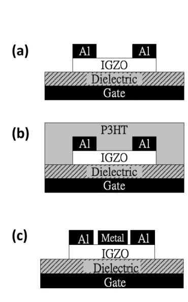
Heavily doped p-type Si (100) was used as a substrate and a gate electrode. Figure 2.1 (a) shows a schematic cross-section of the top-contact bottom-gate a-IGZO TFT structure (b) P3HT-capped the top-contact bottom-gate a-IGZO TFT structure (c) metal-capped the top-contact bottom-gate a-IGZO TFT structure are used in this study. The detail fabrication process including dielectric deposition, a-IGZO film deposition, source/drain deposition, P3HT capping layer deposition and metal capping layer deposition are described in the following sections.
2-1.1 Dielectric deposition
The dielectric silicon nitride (SiNx) was formed on all samples with 1000 Å using Horizontal Furnace. Before deposition the active layer, the standard clean was carried out to remove the contamination on the dielectric surface. The standard clean is accomplished in two steps, SC1 and SC2. SC1 clean is the first step to remove the particle on the surface. The process was executed with a mixture of ammonium hydroxide, an oxidant hydrogen peroxide, and water in a mixing ratio of 1:4:20.
NH4OH:H2O2:H2O = 1:4:20 (SC1)
The SC2 clean was used to remove metals from the surface. The cleaning process in SC2 contain three solution of HCl, hydrogen peroxide, and water. The mixture ratio in the SC2 process was 1:1:6.
2-1.2 a-IGZO film deposition
Generally, pulsed laser deposition (PLD) and ratio frequency (RF) –magnetron sputter were reported to deposit a-IGZO film as channel [10,12]. In this study, the rf-sputter with 3-in. circular target: In2O3:Ga2O3:ZnO = 1:1:1 at.% was used to deposit
the a-IGZO film. 35nm a-IGZO channel layer was deposited at room temperature with a power of 70W, a working pressure of 7mTorr, and an Ar/O2 flow rate of 30/0. The
active layer patterning was defined using a shadow mask.
RF sputtering (Fig. 2.2) is a process using radio frequency power supply, operating at 13.56MHz, to generate plasma in which atoms, ions, and clusters are created to sputter the target material. The glow-discharge between a target and a substrate, it’s consists of plasma with an equal number of working gas (Ar) and electrons. The ions are accelerated towards to the target by a strong electric field on the target due to the flux of electrons. Consequently, the ions hit the target to eject the target atoms, which are then re-deposited onto the substrate. RF sputtering is performed at low pressure, to increase the mean free path, the distance between collisions, and to improve the quality of the deposited film.
2-1.3 Source/Drain deposition
The metal in source/drain contacts was deposited using thermal evaporator. The base pressure of the thermal evaporator is 4×10⁻⁶ torr, and 50nm-thick Aluminum (Al) is deposited through a shadow mask to form the source and drain contacts.
2-1.4 Post-annealing
annealing process at 350 oC in nitrogen (N2) furnace for 1hr, the base pressure is
atmospheric pressure, and the N2 flow rate is 10 liter per minute (L/min).
2-1.5 P3HT capping layer deposition
The poly(3-hexylthiophene) (P3HT) capping layer from chlorobenzene solution (2.5 wt% 2000rpm) was spin coated on the a-IGZO TFT, and baked at 200 oC for 10min. The thickness of P3HT layer is 100nm.
2-1.6 Metal capping layer deposition
The Body metal capping layer on the a-IGZO TFT back channel was deposited using thermal evaporator. The base pressure of the thermal evaporator is 4×10⁻⁶ torr and the thickness of metal capping layer is 50nm.
2-2 Analysis instrument
2-2.1 Current-Voltage measurement instrument
In this study, all electrical characteristics were measured by semiconductor parameter analyzer (Agilent 4156) at room temperature in ambient air.
2-2.2 Light sources
There are five different light sources used to irradiate the device in this thesis. The white light source comes from light-emitting diode (LED) backlight with a broad wavelength range (Fig. 2.3-a). Blue, green, red, infra-red light sources are light-emitting diode with photo-energy from 1.5 eV to 2.8 eV (infra-red to blue) and the spectrum are shown in (Fig. 2.3-b) . The light source is set up above the device to
irradiate the sample from top. The light power is controlled by the power supply (PPT3615) and light blink frequency is controlled by function generator (HP811A). All the measurement under light illumination with the light intensity = 1.2mW/cm2.
2-3 Methods of device parameters extraction
In this section, the extractions of the device parameters are discussed in details. The field effect mobility, threshold voltage (VTH), turn on voltage (Von), the on/off
current ratio (Ion/Ioff), the sub-threshold swing (S.S) are extracted and assessed,
respectively.
2-3.1 Mobility
[29] Mobility is a measurement of the velocity of the carrier move through a material. A higher mobility allows for higher frequency response such as the time it takes for the device to transfer from off state to on state. In the off state, few current flows through the device. In the on state, large amount of currents flow through the device. A large mobility means the device can conduct more current. The mobility in this study was extracted from the saturation region. The device was operated at drain-voltage of 20V, since the threshold voltage was much lower than 20V. The saturation mobility is determined from the transconductance, define by
gm ID
VG V
D const
(2.1) The drift component of drain current is
ID 1
2μCox W
L VGS VTH
2 (2.2)
When the mobility is determined, the transconductance is usually taken to be
When this expression is solved for the mobility, it is known as the saturation mobility μsat 2gm2 W LCox saturation (2.4)
2-3.2 Turn-on voltage (V
on)
Turn-on voltage (Von) is identified as the gate voltage at which the drain current
begins to increase in a transfer curve. Von can directly characterizes the gate voltage
required to fully“turn off"the transistor in a switching application.
2-3.3 Threshold voltage (V
th)
Threshold voltage is related to the operation voltage and power consumptions of TFTs. We extract the threshold voltage from equation (2.5), the intercept point of the square-root of drain current versus voltage when devices operate in saturation mode ID W
LµC X VG V H (2.5)
2-3.4 I
on/I
offcurrent ratio
The Ion/Ioff (on/off) ratio represents large turn-on current and small off current. It
is an indicator of how well a device will work as a switch. A large on/off current ration means there are enough turn-on current to drive the pixel and low off current to maintain in low consumption.
2-3.5 Sub-threshold swing (S.S)
Another important characteristic for device application is sub-threshold swing. It is a measurement of how rapidly the device switches from off state to on state. Moreover,
the sub-threshold swing also represents the interface quality and the defect density [40]. S VG
logID VD const (2-1)
If we want to have a better performance TFTs, we need to lower the sub-threshold swing.
Figure of Chapter 2
Fig. 2.1 The schematic cross-section of the (a) conventional top-contact bottom-gate a-IGZO TFT. (b) P3HT-capped the top-contact bottom-gate a-IGZO TFT. (c) metal-capped the top-contact bottom-gate a-IGZO TFT.
(a)
(b)
Fig. 2.3 The photo-energy spectra of (a) white light LED (b) various light LEDs (blue, green, red, infra-red)
100 200 300 400 500 600 700 800 900 0.0 0.2 0.4 0.6 0.8 1.0
Normaliz
ed Int
e
nsit
y (
a
.u
.)
Wavelength (nm)
White light LED
(a)
1.0 1.5 2.0 2.5 3.0 3.5
0.0 0.5 1.0
Normalized Intensity (a.u.)
Photo-energy (eV)
1.0 1.5 2.0 2.5 3.0 3.5 0.0
0.5 1.0
Normalized Intensity (a.u.)
Photo-energy (eV)
Infra‐red Red Green Blue
Chapter 3
Results and Discussions
3-1 Wavelength and electric field dependent photo-response
on conventional a-IGZO TFT
Amorphous IGZO thin-film transistor has attracted lots of attention for its possible applications on flat, flexible, and transparent display devices. Active matrix liquid crystal display (AM-LCD) and active matrix organic light emitting display (AM-OLED) using a-IGZO TFT array have been demonstrated [46,47]. Therefore, the photo-response to visible light of a-IGZO transistor must be understood. In this section, we discuss the photo-response of a-IGZO TFT under illumination with various wavelengths and find out that a-IGZO TFT is strongly wavelength and operation mode dependent. This study could provide a useful direction for future system design.
3-1.1 Photo
-
sensibility
under illumination with various
wavelengths
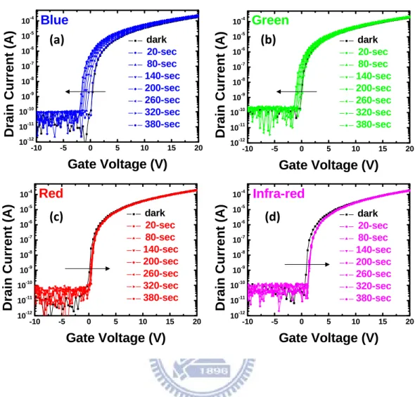
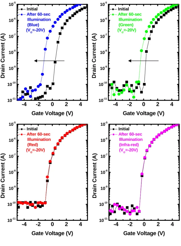
In this experiment, blue, green, red and infra-red light-emitting diodes (LEDs) are used as light sources to discuss the dependence of a-IGZO TFT on light-wavelength. Fig 3.1 shows the photo-energy spectra of various color LEDs, the power intensity on samples of all LEDs is 1.2mW/cm2.
Figs 3.2 show the sequent transfer characteristics of conventional a-IGZO TFT during 380-sec illumination with various colors. As shown in Figs. 3.2(a) and 3.2(b), the transfer curve shift to negative gate bias direction with illumination time when the
conventional a-IGZO TFT is irradiated by blue and green LEDs. On the contrary, as shown in Figs. 3.2(c) and 3.2(d), the sequent transfer curve shift to positive gate bias direction with illumination time when the conventional a-IGZO TFT is irradiated by red and infra-red light LEDs.
The temporal evolution of threshold voltages under various color illumination are shown in Fig. 3.3. The polarity and rate of threshold voltage variation are strongly dependent on the colors. As regard to the light with lower photon energy (red and infra-red), the positively moved threshold voltage attain a saturation value immediately after light-on. As regard to the light with higher photon energy (blue and green), the negatively moved threshold voltage vary relatively larger and does not achieve the saturation in the 380-sec illumination.
According to the results mentioned above, it was found that even the incident light with photo-energy lower than the bandgap of a-IGZO (~3eV), the electric characteristics of a-IGZO TFTs is still obviously influenced. Besides, the light-induced threshold voltage shifts are possibly caused by the competition between two opposite mechanism. One mechanism that dominate in the region of lower photo-energy results in positive threshold voltage shift, and the another one that dominate in the region of higher photo-energy results in negative threshold voltage shift.
3-1.2 Energy-band diagrams of IGZO based MOS under
various gate bias
Since the light-induced threshold voltage shift is possibly caused by two opposite mechanism, the polarity of electric field in IGZO film may be the mechanism. Gate bias adjusts the fermi-level difference between gate electrode and IGZO body. Different polar electric fields enhance trapping in different region. If the electric field
is in the direction of gate, the negative charges are trapped at the interface between dielectric and IGZO active layer that result in positively moved threshold voltage. If the electric field is in the direction of body, negative charges are trapped at body of IGZO active layer that result in negatively moved threshold voltage.
In this experiment, positive and negative bias were applied to the gate terminate of a-IGZO TFT. Fig. 3.4 (a) shows energy band diagram under positive gate bias (VSD=0V, VGS>Vfb). When a positive bias is applied, the lowered fermi-level in the
gate terminate leads to a downward band bending of IGZO active layer near the dielectric interface. As shown in Fig. 3.4 (b), the negative gate bias (VSD=0V, VGS<
Vfb) creates upward band bending in the depletion region of IGZO layer. Then, we
will discuss the electric field effect on a-IGZO TFT accompanied with various color illumination.
3-1.3 Light-induced threshold voltage shift accompanied with
positive gate bias (V
SD=0V, V
GS>
V
fb)
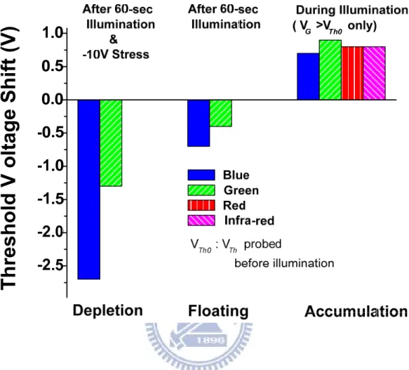
In this section, we discuss the relationship between light-induced threshold voltage shift and operation condition. As shown in Figs. 3.5, all the transfer curves shift to positive gate voltage direction under various color light illumination when the gate voltage lower than flat band voltage are excepted (the transfer curves are probed with gate voltage ranging from 1V to 20V ). A spatial energy-band diagram ranging from gate to IGZO active layer is used to explain the phenomenon as shown in the Fig. 3.8 (a). When a positive gate bias is applied, the lowered fermi level in gate electrode leads to a downward band bending of IGZO active layer near the gate dielectric. The electric field caused by the downward band bending creates trap states. The illuminations
energy. Because the abundant surface states in the band gap, the photons with a wide range of photo energy (ranging from 1.5 eV to 2.8 eV) could be effectively absorbed and then promote the trapping effect under positive bias stress. On the other hand, an illumination with photon energy even much lower than the band gap of IGZO will decrease the drain current if the a-IGZO TFT is operated in on-condition (accumulation condition). The light induced degradation on current may be effectively suppressed by reducing the surface states at the interface between dielectric and active layer of a-IGZO transistor.
3-1.4 Light-induced threshold voltage shift accompanied with
negative gate bias (V
SD=0V, V
GS<
V
fb)
On the contrary, it was found that applying a negative gate bias to the device under blue and green light illumination can obtain a negatively moved threshold voltage. Compare with the result caused by positive gate bias, negative bias causes threshold voltage shift in different direction. As shown in Fig. 3.6, the light-response in depletion condition is examined by 60-sec negative gate-to-source bias stress (VDS=0V, VGS is
-20V) accompanied with various color illuminations. The transfer curves shift to negative voltage direction after blue and green light illumination accompanied with negative gate bias. This phenomenon may be explained by the energy-band diagram in Fig. 3.8 (b), the negative gate bias creates upward band bending in the depletion region in IGZO active layer The electric field derived from the band bending result in carrier trapping. The photons with energy lower than the band gap may be absorbed by the sub-band gap states in bulk. The energy originated from the absorbed photons promotes the electric field induced charge trapping in the bulk of a-IGZO TFT. Although the active range of wavelength is narrow in depletion condition as compared with the one
in accumulation condition, the magnitude of threshold voltage shift is larger. The shallow sub-bandgap states in the bulk permit that only the light with photon energy larger than the one of green light could improve the trapping action.
Fig. 3.7 synthesize the results mentioned above in this study, there are two mechanisms reasonable for positively shifted threshold voltage and negatively shifted threshold voltage under illumination, respectively. The a-IGZO TFT operated in accumulation condition induced carrier trapping that could be assisted by illumination. Similarly, the a-IGZO TFT operated in depletion condition induced carrier trapping that could be assisted by illumination.
In summary, the illumination with photon energy lower than the band gap of a-IGZO could react on the a-IGZO TFTs by promoting both two kinds of carrier trapping.
3-1.5 Rapid charge trapping and de-trapping under light
blink
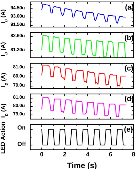
Metal oxide is a material with specific characteristic of higher carrier trapping and de-trapping rate [48]. Usually, the trapping/de-trapping process comprises two parts, one proceeds at high rate and another one proceeds at low rate. Fig. 3.9 shows the real-time response to the 1Hz light blink as the a-IGZO TFT turns on (VGS=15V,
VDS=20V). The result coincide the one mentioned above. All lights with various colors
are active to the a-IGZO TFT. The real-time variation of drain current of a-IGZO TFT indicates the quite fast trapping (light on) and de-trapping (light off) process. As regards to a-IGZO TFT, illumination would induce “minus”-photo current because the drain current decreases as light is turned on.
3-2 P3HT/IGZO hetero-junction
To enhance the visible light photo-sensitivity of a-IGZO TFT, a simple and novel method is proposed to make metal-oxide semiconductor TFT become a visible light photo-transistor with high sensitivity and fast response by capping a polymer semiconductor thin film, P3HT, with high absorption to visible light onto a conventional a-IGZO TFT.
In this study, the mechanism of dissociation of light generated excitons at P3HT/a-IGZO interface should be discussed firstly.
3-2.1 Energy Band diagram of P3HT/ a-IGZO
hetero-junction
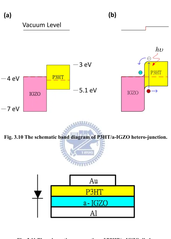
As shown in Fig. 3.10, the P3HT/a-IGZO junction is predicted to be a diode structure with a fermi level difference of approximately 0.3eV [49,50,51] between two terminals. The build-in electric field is predicted to play a role of dissociating electron-hole pairs generated by incident photons.
3-2.2 Rectified I-V Curve
Fig. 3.11 is the schematic diagram of the diode composed of p-type P3HT and n-type a-IGZO. The material of anode and cathode are Au and Al respectively because high work function of Au (5.1 eV) and low work function of Al (4.28 eV). The diode was fabricated on glass by depositing 50nm-thick Al electrode, 35nm thick a-IGZO layer, 100nm-thick P3HT layer and 70nm-thick Au electrode in order, where the a-IGZO layer is deposited by rf sputter and P3HT layer is deposited by spin coating. Fig. 3.12 demonstrates that the a-IGZO/P3HT junction possess a rectifying
characteristic that is similar with the commercial diode. Therefore, a diode characteristic of the P3HT/a-IGZO junction could be confirmed.
3-2.3 Measuring the exciton dissociation at P3HT/a-IGZO
hetero-junction
In order to understand whether the photo-generated electrons could be inject into the a-IGZO side by the build-in electric field in P3HT/IGZO junction or not. A photovoltaic measurement was performed to confirm the exciton dissociation at the p-n junction. Fig. 3.13 shows the framework for photovoltaic measurement. A Nd:YAG laser (λ=266nm) provides a transient illumination with pulse duration of 4 ns to pump the electrons in valance band of IGZO or P3HT. The open circuit voltage of the P3HT/IGZO diode is probed by an oscilloscope. If the build-in electric field could effectively dissociate the photo-generated excitons and then throw the electrons into the IGZO side, the oscilloscope will detect a positive voltage signal as shown in Fig. Fig. 3.14.
Fig. 3.15 presents the temporal evolution of the open circuit voltage of P3HT/IGZO diode. The laser pulse is emitted at the zero second. Dissociated excitons result in an open circuit voltage and then are gradually annihilated with time. The maximum voltage of 0.26 eV is attained during the photovoltaic measurement that indicates a build-in voltage of at least 0.26eV because the maximum probed voltage in theory is equal to the build-in voltage. If the photovoltaic voltage caused by the dissociated excitons totally compensates the build-in voltage in diode, there is no electric field to further dissociate the excitons. As regard to the P3HT/IGZO diode, the full-width-half-maximum (FWHM) of the photovoltaic voltage after laser
(1/4.1ms).
Fig. 3.16 (a) show the real-time photo-response measurement system and Figs. 3.16(b,c) show the real-time photo-responses during an intermittence illumination (λ=470nm) with a frequency of 10Hz and 500Hz respectively. An acceptable frequency around some hundreds Hz is demonstrated.
This section demonstrates that the P3HT/IGZO junction could be a photovoltaic diode to inject light pumped electrons into the IGZO side.
3-3 Photo-transistor based on P3HT-capped a-IGZO TFT
Diode is a common employed light sensor due to the simple structure and fast response. On the contrary, transistor with three terminals is more complicated. However, transistor could provide relatively higher photo-responsivity due to the amplifying characteristic. Field effective transistor (FET) is a voltage control amplifier.In this study, a simple method is proposed to make wide band gap a-IGZO thin film transistors become a visible light photo-transistor with high sensitivity and fast response by capping a polymer semiconductor film, poly (3-hexylthiophene) (P3HT), with high absorption coefficient to visible light onto a conventional top-contact bottom-gate a-IGZO TFT. The visible light-induced threshold voltage shift of P3HT-capped a-IGZO TFT is regard as an input control signal.
3-3.1 The absorption coefficient spectra of P3HT and a-IGZO
thin film
eV. The narrow band gap permit the absorption of light with long wavelength locates in visible region. According to the optical absorption spectra as shown in Fig. 3.17, a-IGZO thin film seems blind in visible light (wavelength longer than 400nm) and P3HT could absorb relatively more in visible light (wavelength range from 400nm to 650nm).
In this experiment, white light-emitting diodes (LEDs) were used as light source to examinat the visible light sensible photo-transistor based on P3HT-capped a-IGZO TFT. Fig 3.18 shows the spectrum of the white LED. The power intensity of white LED on the samples is 1.2mW/cm2.
3-3.2 Sequent transfer curves measuring under white light
Illumination
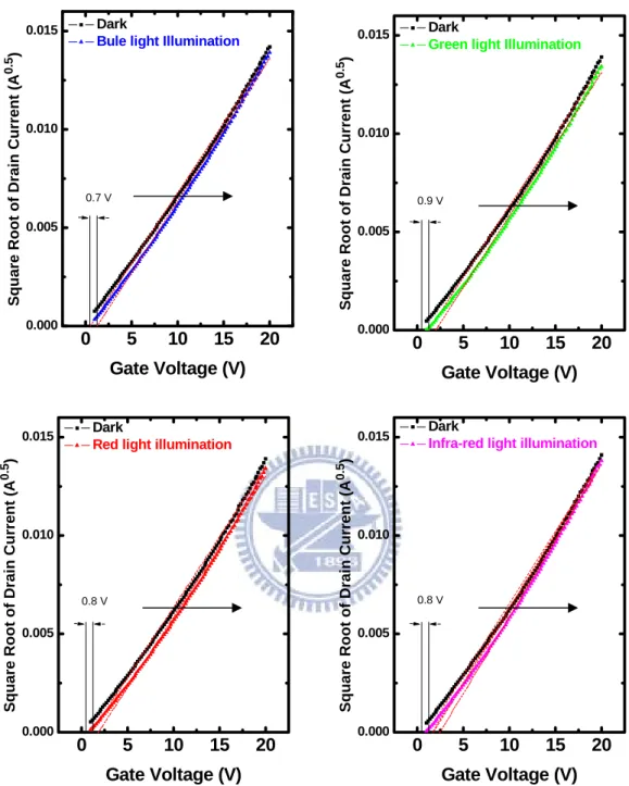
Fig. 3.19(a) presents the transfer characteristics of STD device (conventional a-IGZO TFT) before and during white light illumination. As the illumination starts a series of transfer curves continuously probed in order during 360-sec. Fig. 3.19(b) presents the transfer characteristics of P3HT-capped device. In regard to the STD and P3HT-capped devices, illumination causes a transfer curve shift in negative gate voltage. As compared with the STD device, a significantly transfer curve shift of P3HT-capped device was observed under illumination.
Fig. 3.20 shows the temporal evolution of the threshold voltage shifts of STD and P3HT-capped devices. In regard with P3HT-capped device, a relatively evident response to white light and more than 6 volt threshold voltage shift was observed. Compared to STD device that without P3HT capping layer (threshold voltage shift less than 1volt), the proposed structure with low band gap absorption layer (P3HT)
shown in Fig. 3.20. The P3HT layer is a critical component to promote the ability of visible light sensing in proposed photo-transistor in this study. The function of P3HT layer is not to conduct photo current directly that could be verified by measured photo-current (less than 10-8A) of control device without IGZO layer (P3HT TFT) in Fig. 3.21 P3HT layer may affect the a-IGZO active layer indirectly by separate excitons at P3HT/a-IGZO interface and then induce evident threshold voltage shift of P3HT-capped a-IGZO TFT. As shown in Fig. 3.22, the relationship between threshold voltage shift and illumination time of both STD and P3HT-capped devices are presented together. The threshold voltages were extracted from the transfer characteristics probed in saturation condition (VDS=20V, VGS is scanned from -15V to
20V). P3HT-capped device shows substantial and fast threshold voltage drop during white light illumination 20-sec illumination could make threshold voltage shift more than 3 Volt. The variation from illumination in electric characteristic of P3HT-capped photo-transistor almost belongs to threshold voltage shift by comparing the transfer curves probed after various period illuminations as shown in Fig. 3.23.
3-3.3 Significant photo-responsivity of P3HT-capped a-IGZO
TFT caused by threshold voltage shift
The photo-responsitivity (Rph) as a function of gate bias of P3HT-capped
photo-transistor and STD device are demonstrated in Fig. 3.24. Rph is defined by
Iph/(EWL), where Iph is photocurrent (drain current under illumination minus drain
current in initially dark condition), E is power intensity of incident light (W/cm2). Measurements are taken after 20-sec and 120-sec white light illumination (1.2 mW/cm2). Rph is strongly dependent on the gate voltage that indicates light-induced
photo-responsitivity of P3HT-capped a-IGZO TFT could achieve as high as 4A/W after 20-sec illumination. On the contrary, STD device present quite small photo-responsitivity. According to the results, P3HT layer plays a critical role in the visible light sensibility. P3HT-capped a-IGZO TFT possesses high drain current difference before and after illumination at one gate voltage point that satisfy the requirement of photo-detector.
3-3.4 Real-time drain-current sampling under light blinked
illumination.
As compared to STD device, the transfer of light-induced threshold voltage shift caused by exciton separation at P3HT/a-IGZO interface in proposed photo-transistor is much fast and evident. The continuous drain current sampling measurements of both P3HT-capped photo-transistor and STD device in turn-on conditions (VDS= 1V,
5V, 10V and 20V, VGS=15V) were performed and presented in Figs. 3.25 (a) and 3.25
(b). The white light source is blinked with alternate frequency of 1 Hz as shown in Fig 3.25 (c). The power density of white light on the sample’s surface is 1.2 mW/cm2 during light-on period. Obviously, the STD device could not follow the variation of light source due to the stable threshold voltage under light blink. On the contrary, the P3HT-capped photo-transistor performs high real-time sensibility. 20μA drain current difference between light and dark period for P3HT-capped photo-transistor in the condition with 20V VDS. 20μA variation of drain current indicates about 3 Volt
threshold voltage vibration amplitude (estimated by the conductance of transfer curve) and 5A/W real-time photo-responsibility (1Hz).
carrier injection from P3HT. For P3HT-capped device, the evident threshold voltage shift is possibly resulted from exciton separation at P3HT/IGZO interface. Besides, the huge photo-response of P3HT-capped photo-transistor may be resulted from the injected electrons that accumulation at back channel to enhance trapping probability in depletion region.
3-3.5 The proposed mechanism of light-induced threshold
voltage
In this study, P3HT capping layer is employed as the light absorption layer to perform light sensing action in photo-transistor. However, narrow band gap is not the only requirement for material selection. The interface between IGZO active layer and photo-absorption layer is also critical. Interface between IGZO and absorption layer must possess adequate ability to dissociate photo-generated exaction and then inject electrons into IGZO active layer. p-n junction with build-in electric field is an effective structure to dissociate excitons and is generally employed in photo-voltaic devices. The interface between p-type P3HT and n-type IGZO may form a p-n diode structure with vacuum level difference of 0.3eV as the contact is formed [4,5]. The vacuum level difference means an electric field exists with a direction from IGZO to P3HT. The function of P3HT layer in photo-transistor is to introduce photo-generated electrons into IGZO active layer. The spatial energy-band diagrams of the P3HT -capped IGZO photo-transistor under different operation conditions are presented in Fig. 3-3.9 (a) and (b). The photo-transistor could be considered one device comprised of a field effective transistor and a photo-diode. IGZO layer is employed as both active layer in transistor and n-layer in p-n junction, the p-n junction could absorb visible light and then affect the body voltage of transistor.
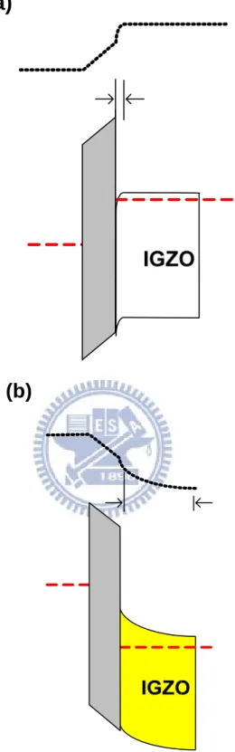
The mechanism of threshold voltage shift induced by illumination is proposed and also sketched in Fig. 3.26. Photons of visible light pump the electrons from valence band to conduction band in P3HT layer and then drift into the IGZO active layer by internally build-in electric field at the interface between IGZO and P3HT layers. Then, the P3HT introduced electrons is accumulated at the back channel in IGZO layer and result in threshold voltage shift by body effect. In particular, the electron accumulation at back channel mainly occurs while a depletion region formed along the length between source and drain. In depletion region, an electric field exists to make electron accumulation at back channel as shown in Fig. 3.26 (a). On the other hand, the threshold voltage will keep unchanging in accumulation condition during illumination as shown in Fig. 3.26 (b). The energy band is flat in the bulk of IGZO layer.
To verify the proposed mechanism mentioned above, a series of experiments are made to make sure the effect of electric field in bulk of IGZO layer on photo-response. First, a 60-sec illumination accompanied with floating electrodes is performed as shown in Fig. 3.27 (a). There is no measured light-induced threshold voltage shift as shown in Fig. 3.28 (a). In other words, the P3HT-capped a-IGZO TFT would not be influenced by illumination if the device doesn’t operate. Second, an 60-sec illumination accompanied with positive gate bias stress (VDS=0V, VGS>0V) is
performed as shown in Fig. 3.27(b). A channel form along the device length and the energy band in the body is flat. There is no measured light-induced threshold voltage shift as shown in Fig. 3.28 (b). In other words, the P3HT-capped a-IGZO TFT would not be influenced by illumination if there is no electric fields in the back channel even the device is turned on. Third, an 60-sec illumination accompanied negative gate bias stress (VDS=0V, VGS<0V) is performed as shown in Fig. 3.27(c). A depletion region
appears during the illumination. There is an electric field exists in the body of a-IGZO TFT. As shown in Fig. 3.28 (c), a significant light-induced threshold voltage shift measured after illumination. The light-induced threshold voltage shift is referred to the electron accumulation at the back channel of IGZO active layer and P3HT/IGZO junction play a role to introduce electrons. In a word, the depletion region with electric field is an area to trap electrons that has been assumed in section 3.1 and the P3HT/IGZO hetero junction is used to provide light pumped electrons for trapping.
According to the result mentioned above, the depletion region is required to sense the visible light. The length have to be fully (subject negative gate bias stress, VDS= 0V, VGS<0V) or partially (device is operated in saturation condition, VDS>
VGS-Vth) depleted (channel is pinched-off by depletion region near drain) to sense the
light by threshold voltage shift as shown in Fig. 3.29.
Depletion region is required for P3HT-capped a-IGZO TFT to sense the visible light. However, n-channel IGZO TFT must be operated in accumulation condition to form an electron channel. Therefore, saturation operation mode (length is partially depleted and partially electron-accumulated) is demanded for real-time light sensing process. Corresponding to the result shown in Fig. 3.25, the valid real-time light sensing performance of the P3HT capped photo-transistor is examined under the saturation condition (VGS=15V, VDS=20V >VGS -Vth=9V). On the contrary, no
photo-signal is observed if the device is operated under linear condition (VGS=15V,
VDS=1V <VGS -Vth=9V). Depletion region (electric field exist in IGZO body) in the
length of P3HT capped photo-transistor is essential for sensing visible light as shown in Fig. 3.29 (b).
The entire sensing procedure possibly comprises three phases. First, excitons are generated in P3HT layer by visible light. Second, the excitons are dissociated at
P3HT/IGZO hetero-junction by initially build-in electric field and then electrons are introduced into IGZO layer. Third, the light introduced electrons are accumulated at the back channel of IGZO layer with pinched-off channel. The negative charges (comprised of accumulated electrons) at back channel would make threshold voltage decreasing. Decreased threshold voltage induced by illumination indicates the higher drain current at one gate voltage.
3-4 A novel approach to modify the threshold voltage of
a-IGZO TFT by capping metallic layer on active layer
3-4.1 Motivation
According to the experiment result mentioned above, a 6.1V threshold voltage shift of P3HT-capped a-IGZO TFT in the direction of positive gate voltage was observed after capping P3HT layer onto the active layer of bottom-gate a-IGZO TFT as shown in Fig.3.30. In this section, an energy-band diagram is proposed to explain this phenomenon. Fig. 3.31(a) presents that the fermi-level of IGZO and P3HT is different before contact. The fermi-level of p-type P3HT semiconductor layer is lower than the one in IGZO. During the IGZO and P3HT contacting process, the fermi levels of two layers should be adjusted to the same due to both sides of the system must reach equilibration as shown in Fig. 3.31(b). During contacting, the electrons in IGZO will flow down into P3HT. It is speculated that electric dipoles are formed at the P3HT/IGZO junction to bend the vacuum level across two sides. The bended vacuum level leads to an equivalent fermi-level across the whole device. The dipoles at the back channel of a-IGZO transistor result in an adjusted threshold voltage. Then, we
demonstrate that the threshold voltage position of a-IGZO TFT could be effectively adjusted by capping layer with various work functions.
3-4.2 Threshold voltage turning by capping metallic layer
with various work function
A series of metal layers with various work functions are employed to modulate the threshold voltage of a-IGZO TFT in this study. The metal layer with a specific work function is capping on the active layer of bottom-gate top-contact IGZO TFT to move the threshold voltage in the desired distance. The metal layer is located between two contact electrodes with gaps of 150μm. In other words, the 300μm-long length is half covered by a metal layer. The transfer characteristics of a-IGZO TFT with and without Au layer capping are shown together in Fig. 3.32. A threshold voltage shift of 5.1 volt is attained after 70nm-thick Au layer is capped onto a-IGZO TFT. The work function of Au is 5.1eV that is larger than the one of a-IGZO, therefore the electrons will flow from the a-IGZO to Au to form electrode dipoles. The Au layer depletes the active layer and then makes a positively moved threshold voltage that is similar with P3HT. This mechanism could be schematically explained by energy-band diagrams in Figs. 3.33. The charge re-distribution at the junction between metal and IGZO layers results in a body effect on IGZO TFT to modulate the threshold voltage. When dipoles form, the dipole induced voltage drop appear across the body. The threshold voltage position is positively moved by the body effect with positive source to body bias (VSB>0) while the
Au is employed. This result demonstrates that the threshold voltage position of a-IGZO TFT could be effectively adjusted by capping metal layers with various work functions. Fig. 3.34 presents the threshold voltage shifts plotted as a function of work function of metal capping layer. The adjustable threshold voltage shift could be ranged from -6V to
6V. Table 3.1 lists the typical parameters such as mobility, threshold voltage (VTH),
threshold voltage shift (ΔVTH), ION/IOFF current ratio, and sub-threshold swing (S.S).
Besides, the work function of a-IGZO is estimated to be 4.33eV~4.65eV by the polarity transfer point of threshold voltage shift is located between Ti (4.33eV) and Cu (4.65eV). As shown in Fig. 3.35 and Fig. 3.36, the metal capping method also provides a powerful solution to double the mobility without causing current leakage and performance degradation. Fig. 3.37 and Fig. 3.38 present the transfer characteristics that after capping Ti (4.33eV) layer on the active layer of bottom-gate top-contact IGZO TFT, the device performance was significantly improved by capping Ti metal layer, an excellent sub-threshold swing value of 0.18 V/decade, threshold voltage of 1.6 volt, and high IOn/IOff ratio of 5×10⁹, the field-effect mobility was enhanced from
9.04 to 18.2 cm2/Vs.
The device mobility improvement is unclear and might be belonged to strain effect. In previous research, straining lattice changes the inter-atomic spacing, the associated changes in band structure and density of states contribute to mobility improvement in transistors [52]. Therefore, this simple and novel method based on metallic capping on metal oxide transistor could effectively modulate the threshold voltage position and enhance the device performance.
Figure of Chapter 3
Fig. 3.1 The LEDs Photo-energy spectra.
1.0 1.5 2.0 2.5 3.0 3.5
0.0 0.5 1.0
![Fig. 1.1 The carrier transport paths in covalent semiconductors [7].](https://thumb-ap.123doks.com/thumbv2/9libinfo/8388114.178568/22.892.273.604.557.869/fig-carrier-transport-paths-covalent-semiconductors.webp)