中文摘要
隨 著 無 線 通 訊 市 場 的 成 長 和 可 攜 式 3C 應 用 系 統 的 普 及 化 , 高 速 無 線 傳 輸 成 為 一 個 必 然 的 趨 勢 。 在此三年的研究計畫中,我們先針對目前使用於 ISM 頻帶的基 頻調變技術以及通道進行分析和研究,我們所進行的方式為使用高階模擬軟體, 分析現今 常見的無線區域網路系統的調變技術—如 Bluetooth 中的跳頻方式與 WLAN 中的 CCK 和 OFDM —於不同的傳輸通道(包含 AWGN 與 Rayleigh Multipath Fading)之效能表現,我們同 時探討這些解調變方式在經由量化(quantization)之後和理論值的出入,以及如何提升同步的 能力以改善系統傳輸的品質。由過去的系統研發經驗,我 們 體 會 到 基 頻 電 路 設 計 和 其 他 子 系 統 ( RF/IF 與 MAC)有 密 不 可 分 的 關 係, 因 此 本 計 畫 中, 我 們 也 進 行 了 各 調 變 方 式 與 介 質 存 取 控 制 模 組 之 整 合 系 統 模 擬。目 前 之 無 線 數 據 網 路 規 約如 IEEE 802. 11的 介 質 存 取 控 制 積 體 電 路 , 多 是 以 處 理 器 為 基 礎 設 計 , 將 大 部 份 的 介 質 多 工 存 取 層 與 實 體 層 的 標 準,例 如 具 碰 撞 避 免 功 能 的 分 立 架 構 無 線 載 波 偵 測 多 重 存 取 (CS MA/CA) , 以 嵌 入 碼 的 方 式 實 現 , 例 如 以 80188 處 理 器 為 基 礎 的 AMD79C30 與 DSP 處 理 器 為 主 軸 的 HFA3841。這 與 乙 太 網 路 的 介 質 存 取 控 制 積 體 電 路 所 採 用 的, 針 對 協 定 特 定 設 計 的 方 式,有 著 極 大 的 不 同。此 種 設 計 方 式 , 固 然 有 「 韌 體 程 式 修 改 維 護 方 便 」 與 「 Protoco l 更 新 時 , 免 除 重 新 設 計 積 體 電 路 」的 優 點, 卻 也 帶 來 了 韌 體 運 算 速 度 受 限 於 處 理 器 速 度,迫 使 在 追 求 高 速 數 據 傳 輸 時,必 需 採 用 高 運 算 速 度 處 理 器 來 作 為 設 計 核 心,相 對 的 影 響 整 體 的 成 本 效 益 。 更 重 要 的 是 ,「 以 處 理 器 為 核 心 之 MAC 模 組 設 計 」 在 與 Bas e ba nd 甚 至 R F/IF 作 單 晶 片 整 合 時,將 不 易 進 行 整 體 單 晶 片 的 系 統 模 擬。基 於 此 , 我 們 針 對 IEEE 802.11 所 規 範 的 具 碰 撞 避 免 功 能 的 分 立 架 構 無 線 載 波 偵 測 多 重 存 取,與 需 及 時 處 理 的 控 制 框 架 (Cont rol Fr ame)如 RTS/CTS 與 ACK, 乃 至 於 與 經 常 處 理 的 管 理 框 架 ( Management Frame),設 計 一 個 專 用 的 無 線 數 據 網 路 介 質 存 取 控 制 積 體 電 路 電 路 模 組 , 並 將 包 含 「 高 速 平 行 CRC 線 路 架 構 」 [8] 與 「 Do uble Bu ffer ing 架 構 」, 以 達 到 高 速 (>10 0M bps)傳 輸 的 目 標 。 我 們 於 第 一 年 完 成 高 速 無 線 數 據 存 取 控 制 與 基 頻 收 發 各 積 體 電 路 子 模 組 的 界 面 規 劃 與 設 計 , 以 及 ISM 頻帶的基頻調變技術以及通道的分析和評估。 第 二 年 的 計 畫 則 著 重 在 核 心 技 術 的 發 展 與 系 統 整 合 ; 於 基 頻 方 面 , 我 們 設計了一個互補式編碼調變 的 11Mbps 無線區域網路基頻處理晶片,並利用 SPW 做系統性能驗證及評估,最後再以 Verilog 做實體層的系統模擬。為了使介質存取控制器與 基 頻 處 理 器 能 整 合 於 單 一 晶 片 上 , 介質存取控制器以 標準單元式積體電路為架構,並以 ARM 為控制核心進行設計,在 此架構下我 們 用 純 組 合 邏 輯 設 計 達 成 IEEE 802.11 所 規 範 的 具 碰 撞 避 免 功 能 的 分 立 架 構 無 線 載 波 偵 測 多 重 存 取,同 時 也 用 組 合 邏 輯 處 理 需 及 時 處 理 的 控 制 框 架 與 管 理 框 架 。 在 基 頻 與 介 質 存 取 模 組 的 介 面 上 , 採 用 高 速 FI FO 的 架 構 , 在 製 程 的 模 擬 上 確 實 達 到 100Mbps 以 上 的 傳 輸 速 度 。 在第三年的計畫,我們提出並 實作一個新的 CCK 基頻同步演算法,同時為驗證我們所設計的基頻與介質存取模組之單晶 片整合的可行性,我們除了進行系統整合模擬,並於兩套 ARM Evaluation Board 與其上的 FPGA 上完成互傳測試。
關鍵詞:無線高速數據網路、分立架構無線載波偵測多重存取、正交分頻多工、互補碼、
跳頻展頻、直接序列展頻
英文摘要
The rec e nt gro wt h o f w ir e le ss co mmu n ic at io n mark et and t he w ide- spre ad o f po rt able 3C a pp licat io ns make hig h- spe ed w ir e le ss t rans mis s io n a pro mis in g fut ure t echno lo g y. I n t his t hr ee- ye ar pro ject , we beg a n w it h t he p er fo r ma nc e e va luat io n a nd a na lys is fo r var io us ISM ba nd mo du lat io n t ec hnique s t rans mit t ed o ver c ha nne ls w it h d iver se c haract er ist ics. T he c ha nne ls co ns idere d inc lu de d AWGN channel and Rayleigh multipath fading channel. The ISM band modulation techniques covered the FHSS modulation specified in Bluetooth system, and CCK and OFDM modulations employed in WLAN. Performance degradation due to quantization, as well as imperfect synchronization, was also investigated. From our past experience in system development, the design of baseband tranceiver is tightly related to other system modules, such as RF/IF and MAC. Accordingly, we performed the system-level integration of MAC and baseband transceiver in order to examine their joint workability. The MAC design of the existing IEEE 802.11 products mostly employed a CPU-based design methodology, which implements the CSMA/CA module in terms of executing embedded code in an embedded CPU. Two known examples are the 80188-based AMD79C930 and the DSP-based HFA3841. Although such a firmware-based implementation is easy in its maintenance and flexible to standard revision, it unavoidably renders a dilemma between processing speed and cost. Most importantly, a firmware-based MAC design hardens the joint simulations with RF/IF and baseband modules. We therefore took an alternative design strategy, namely to cost-effectively partition between the hardware components for MAC and its associated software modules executed at host (in a form of a driver). Our hardware MAC modules include the CSMA/CA Unit, Control Frame Handling Unit, High-Speed CRC Unit, and Double-Buffering Memory Unit. The targeted transmission speed 100Mbps was then successfully achieved. In the first year, we finished the interface design and determined the partitions of submodules for our integrated MAC and baseband tranceiver chip. Performance evaluations for various channels and transmission techniques were also done in this year. In the second year, we turned to the detailed development of each submodule. In summary, a CCK 11Mbps baseband chip has been developed, and subsequently simulated under SPW. To integrate the MAC and baseband modules in a chip, MAC was developed by pure combinational logics with an embedded ARM for upper-protocol applications. Under such a system setting, CSMA/CA and the handle of control and time-critical management frames are all performed by pure combinational logics. A FIFO interface between MAC and baseband modules was adopted to maintain a 100Mbps transmission rate. In the third year, we proposed and implemented a novel synchronization algorithm for CCK modulation. Meanwhile, in order to test the feasibility of our integrated MAC/BB chip, we not only conducted joint simulations, but also examined our design though on-line transceiving over two ARM Evaluation Boards.
Keywords: High-Speed Wireless Data Networks、CSMA/CD、OFDM、CCK、FHSS、DSSS
目 錄
一、前言 1
二、研究目的 2
三、研究方法 4
四、結果與討論 6
五、參考文獻 17
六、研究成果自評 19
附錄一、可供推廣之研發成果資料表
III一、前言
After the Standard Committee of IEEE Society drew up the Wireless LAN 802.11 specification in 1997 [1], wireless LAN gradually became a favored link in indoor environments, such as office buildings, hospitals, factories, etc. This standard specifies the Medium Access Control (MAC) layer that selectively supports one of the three physical layer units, i.e., the direct sequence spread spectrum (DSSS) radio unit, the frequency hopping spread spectrum (FHSS) radio unit, and the Baseband infrared unit. Both radio units operate in 2.4GHz industrial, scientific and medical (ISM) band. At its first standardization, the IEEE802.11 DSSS radio unit simply provides 1 Mbps and 2 Mbps nominal data rates. Due to the growing demand for higher transmission speed, the same organization proposed an extension standard for the DSSS physical layer, which employs 8-chip complementary code keying (CCK) modulation, and results in two higher rates of 5.5 Mbps and 11 Mbps in addition to the 1 Mbps and 2 Mbps [2]. To minimize the extra system cost due to standard migration, the extension standard uses the same frequency allocation and signal bandwidth.
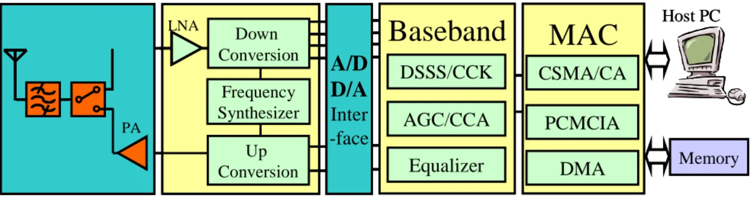
This project intends to develop a WLAN system that conforms to the IEEE802.11 a/b/g standards [1, 2]. To facilitate the system development, the taskforces, as well as the system diagram, have been functionally partitioned into RF, Baseband, MAC and Software (See Figure 1). The main focus of this subject is on the integration of the Baseband and MAC modules.
MAC
LNA Up Conversion Frequency Synthesizer Down ConversionA/D
D/A
Inter -faceBaseband
Memory Host PC PA DSSS/CCK AGC/CCA Equalizer CSMA/CA PCMCIA DMAMAC
LNA Up Conversion Frequency Synthesizer Down ConversionA/D
D/A
Inter -faceBaseband
Memory Host PC PA PA DSSS/CCK AGC/CCA Equalizer CSMA/CA PCMCIA DMAFigure 1: System diagram of a sample WLAN design.
二、研究目的
The current implementations of the IEEE 802.11 Medium Access Control (MAC) mostly incorporate a CPU core in their integrated circuit designs, where the MAC protocol is realized through firmware implementation. Two renowned examples are the AMD79C30 and HFA3842 MAC controllers. The former employs an embedded 80188 core, while the latter incorporates a micro-programmed MAC engine. As the IEEE802.11 MAC standard [1, 2, 3] converges to DFW CSMA/CA, and no further revision on the underlying MAC standard is in process, the need of flexibility and customization on the MAC design gradually migrates to the demand of a cost-effective design, i.e., a design that can achieve high speed with a fairly low cost. This motivates us to develop a pure combinational-logic-based MAC controller and to integrate the MAC with the Baseband module.
Different from the Ethernet standard, the MAC specified in IEEE802.11 requires more management efforts (in addition to the basic CSMA/CA mechanism) due to the unreliable nature of wireless transmissions. The ability to handle the control frames and the management frames are therefore essential to an IEEE802.11 MAC controller. Perhaps, this is the key reason why the firmware-based implementation approach is more prevalent on the market. For example, a timely layer-2 acknowledgement and re-transmission due to previous transmission failure are specified in the standard. To fulfill the management requirement, a separate Control Frame Handler circuit is designed to manipulate the timely transmission and response of the control frames, such as RTS, CTS and ACK frames. This unit closely co-works with other units under the finite-state machine on which our design is based, and complements the management functionality of the IEEE802.11. A second revision of our MAC verilog code additionally includes the manipulation of some time-critical management frames (which was previously designed to be handled by the host driver) to further enhance the system performance.
Our previous experimental design was carried out in two stages, which yielded two versions of MAC verilog codes. In the first stage, we only attempted to substantiate the idea of realizing the IEEE802.11 MAC protocol using pure combinational logics, and only targeting the 1/2 Mbps basic processing speed of IEEE802.11 MAC [4, 5]. After its effectiveness, a major revision on the
previous version is subsequently preceded, which results in an over-100 Mbps data rate to-and-from the baseband processor [6]. A third revision was then conducted in this project to refine the PCMCIA interface [7] to AMBA interface to facility the on-tine transceiving test over an ARM evaluation boards, and also to facilitate the application software such as MPEG to execute on top of our prototypes. Although the current standard only specifies up to 54 Mbps nominal data rate [3], our experimental implementation does confirm the feasibility and cost-effectiveness of a combinational logic design of an IEEE802.11 MAC.
It is worth mentioning that a pure combinational logic design of the IEEE802.11 MAC also facilitates the chip-level integration with the baseband processor. Since both the MAC and the baseband circuits are implemented directly using the verilog language, a cell-level joint-simulation can be readily performed in an on-line transceiving fashion, which largely ensures the workability of the resultant integrated MAC/baseband processor. Specifically, one can employ two joint-modules of MAC and baseband circuits, and simulate the on-line exchange of the sequence of RTS, CTS, data and ACK frames.
Another objective of this project is to develop an efficient baseband submodule for use of wireless LAN system. It began with the examination of imperfection impact, such as quantization, on baseband design, and ended at the provision of a novel synchronization algorithm. Details will be provided in subsequent sections.
三、研究方法
The IEEE802.11b PHY is one of the PHY layer extensions of IEEE802.11, and is referred to as the high rate direct sequence spread spectrum (HR/DSSS). The HR/DSSS uses the same preamble and header frame as the IEEE802.11 PHY, which is sent at 1Mbps using DBPSK and Barker code direct sequence spreading. There are four kinds of data rate specified. The DSSS with DBPSK and DQPSK modulation supports 1Mbps and 2Mbps communications, while the CCK modulation supports 5.5Mbps and 11Mbps communications. For HR/DSSS, the CCK code is employed with the same occupied channel bandwidth as DSSS. The CCK code has a code length of 8 chips, where 256 possible sequences can be constructed using 4 QPSK phases—1 to
4. Eight information bits (d0 to d7, d0 first in time) are transmitted per symbol. {d0, d1}
encodes1 based on DQPSK, but “odd symbol” must rotates 180 degree to optimize the sequence
correlation and to minimize DC offsets in the codes. {d2, d3}, {d4, d5} and {d6, d7} respectively
encodes 2, 3 and 4 based on QPSK. The four terms: 1, 2, 3 and 4 are the main factors
constituting the CCK codeword. The CCK code has poor auto-correlation and cross-correlation characters, and it is hard to detect the symbol boundary since the CCK code-spreading pattern varies with the transmitted data. Hence, the CCK code relies on the initial timing and phase tracking information obtained from the preamble sequence, which is transmitted by the fixed-pattern Barker code direct sequence spreading.
For the baseband CCK modulation technique, a conventional design is to use the Direct Matched Filter (DMF). A more recent and nowadays popular design for CCK modulation is to employ the concept of Fast Walsh Transform (FWT). In this subproject, a novel structure of Differential Phase Transform (DPT) was proposed and implemented.
Among the aforementioned three structures for CCK modulation, DMF has the best performance; but its performance cannot sustain highly involved noises due to complex environment. FWT performs a little worse than DMF; it is however more cost-economy from the viewpoint of hardware implementation. DPT performs worse among the three structures, yet it consumes the least hardware cost. As power economy is essential for WLAN system, the DPT should be a suitable and justifiable choice.
On the other hand, most of the current Wireless LAN Medium Access Control (MAC) modules incorporate a CPU-core in their integrated circuits, where the IEEE802.11 MAC protocol is fulfilled through firmware implementation. Such implementation approach is certain to be flexible for customization design. Two known examples are the AMD79C30 and HFA3842 MAC controllers. The former employs an embedded 80188 core, while the latter incorporates a micro-programmed MAC engine.
Our cell-based design, however, implements the MAC protocol completely by logic combination circuits [4, 5, 6, 9]. As the IEEE802.11 MAC standard converges to DFW CSMA/CA, and no further revision on the underlying MAC standard is in process, the combination-logic implementation approach should bring one with the benefits of low cost and high speed, when being compared to the firmware-based implementation. It also facilitates the chip-level integration with the Baseband processor. Yet, when a major revision on the MAC standard occurs, such implementation approach unavoidably suffers a higher re-design effort.
In order to amend the inflexibility of hardware MAC, we adopted a modularized structural design with internal (inter-functional-unit) bus. The connection of our MAC to host is through a standardized HIU functional unit. This will facilitate the scalability of our MAC to other host interfaces, such as PCI and AMBA. Our MAC also adopted an external SRAM for the temporary storage of transceiving data, and interfaced with the SRAM through an independent Btag functional unit. This will greatly release the switch burden between different types of memory chips. Besides, when a new functional unit becomes necessary due to the revision of IEEE 802.11 standard, we can easily adjust our MAC structure by interconnecting this new functional unit through the internal bus. With a modularized structure, our MAC provides a portable design, and can be easily adjusted to fulfill the various demands of transmission speed and host interface.
四、結果與討論
The function of the baseband transmitter is to encode the data stream from the MAC section to the Barker code or CCK code, and then transmit the respective analog signal to the RF section. The baseband receiver is to receive the analog signal from RF section and recover the data stream to the MAC section. Because of the usage of spread spectrum technology, the receiver must despread the signal, sample the “peak information” properly, and then differentially decode the data.
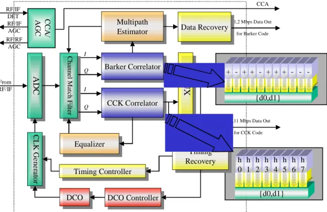
Our proposed architecture of the IEEE802.11b baseband processor can be described as follows as shown in Fig. 2. We adopt 5-bit resolution ADC working at 44 MSPS. The Channel Match Filter stores the sampled data and compensates multipath effect estimated by the Multipath Estimator. The Multipath Estimator calculates the channel impulse response simply for Barker codes. For CCK codes, the Equalizer is used instead. The Barker Correlator and the CCK Correlator compute the signal power to determine which one is received, and provide necessary information for data recovery and timing recovery. We use “Early-Late” architecture in Timing Recovery to synchronize the sampling rate and phase offset, in case there is any sampling time error. The Clock Generator generates sampling clock phase, which is controlled by the Timing Controller based on the output of Digitally Controlled Oscillator (DCO). If the sampling frequency errors occur, DCO controller will increase or decrease the DCO output clock rate to compensate them. The CCA/AGC (Clear Channel Assessment/Auto Gain Control) locating at the left-top corner of Fig. 2 is auxiliarily significant to the system integration. The AGC adjusts the power level in the RF section, and the CCA monitors the environment to determine the channel status for usage by the MAC section.
A D C A D C CCK Correlator CCK Correlator DCO
DCO DCO ControllerDCO Controller Multipath Estimator Multipath Estimator Timing Recovery Timing Recovery Data Recovery Data Recovery Barker Correlator Barker Correlator M U X M U X Equalizer Equalizer C han n el Mat ch F ilt er C hann el Mat ch F ilt er CL K G en er ato r CL K Ge n e ra to
r Timing ControllerTiming Controller
1,2 Mbps Data Out for Barker Code
5.5,11 Mbps Data Out for CCK Code I I Q Q From RF/IF {d0,d1} + + + + + + -{d0,d1} h 0 h 1 h 2 h 3 h 4 h 5 h 6 h 7 CCA / A G C RF/IF DET RF/IF AGC CCA RF/RF AGC
Figure 2: IEEE802.11b wireless LAN baseband design.
Although the FWT (Fast Walsh Transform) is commonly used to construct the CCK demodulator, we take the DPT (Differential Phase Transform) [10] algorithm instead. From our experiments, the DPT-based CCK demodulator, because of its weighting factor, has better BER than the FWT-based CCK demodulator. Furthermore, the DPT-based CCK demodulator can extract the information of frequency offset without extra chip area. On the other hand, for the receiver with frequency error effect, the phase of the received signal vectors will spin, and the rotating phase will accumulate continuously. We use the two neighboring chips to get the phase offset produced by the carrier frequency offset, and compensate the errors by phase rotator.
The encoding process of CCK codes can be expressed as shown in Eq. (1).
} , , , , , , , { ) 4 , 3 , 2 , 1 ( 1 ) 2 1 ( ) 3 1 ( ) 3 2 1 ( ) 4 1 ( ) 4 2 1 ( ) 4 3 1 ( ) 4 3 2 1 ( a j a a j a a j a a a j a a j a a a j a a a j a a a a j ha a e e e e e e e e a a a a C S (1)
In short, the symbol of CCK code consists of eight chip, C0a~C7a, where a is the time index. The
information is contained in the phases of the CCK symbol, i.e., 1 ~ 4. Equation (2) illustrates the mathematical relation of DMF:
7 0 * 7 [ 1, 2, 3, 4] ] [ }] 4 , 3 , 2 , 1 { , [ k k c cck n r n kT C V (2)where Vcck represents the decision vectors of the correlator output, Tc is the chip duration, r[n] is
the baseband received signal, Cx(θ1, θ2, θ3, θ4) is the predictions of the CCK symbol. Notably,
Cx(θ1, θ2, θ3, θ4) is actually dependent on the estimates of phases θ1, θ2, θ3, θ4 at time
instance x.
The FWT formula for CCK modulation can be defined as:
1
(5) ) 4 ( 1 0 0 0 0 1 ) 3 ( 1 0 0 0 0 0 0 0 0 1 0 0 0 0 0 0 0 0 1 0 0 0 0 0 0 0 0 1 3 2 1 C H B B H A A A A H where {A,B,C = e{jθ2}, e{jθ3}, e{jθ4}}, respectively. In practice, the receiver can have an estimate of 1 ~ 4 by locating the maximum of T T T
aH H H
S 1 2 3 .
What we proposed is the DPT, which can be expressed as:
and
We summarizes the hardware consumption analysis of the above three modulations in Tab. 1. In this table, Cor. is the number of correlators, C-Add/Mul represents the number of complex adder/multiplier, and M.P. is the number of Maximum Picker. We found that DMT has the highest hardware consumption – 51K, FWT can reduce its hardware consumption down to half, and
DPT can further half the hardware consumption of FWT by taking advantage of its highly parallel character. The resultant hardware consumption of DPT is around 13K only. Notably, we can also share the hardware among several DPT function units, and largely reduce its hardware consumption to 4K. In summary, our CCK demodulator only requires 4K logical gates for its implementation, which is 90% less than the DMF and 80% less than the FWT.
Table 1: The hardware consumption analysis summary of various CCK modulators.
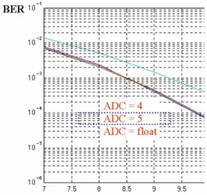
Of course, we need to consider the quantization imperfection in practice. By implementing the demodulator using the verilog language, we can effectively simulate the number of quantization levels required to achieve an acceptable performance. As shown in Figure 3, after testing 3-bit, 4-bit and 5-bit quantizations, we found that 4-bit quantization is sufficient to achieve the prefect performance without quantization. We however take 5-bit quantization in our design for a better system robustness and reliability.
Figure 3: Quantization impact on DPT demodulator.
After finishing the design and practice the CCK demodulator in the previous two years, we turn to the synchronization in our third year.
Frequency synchronization
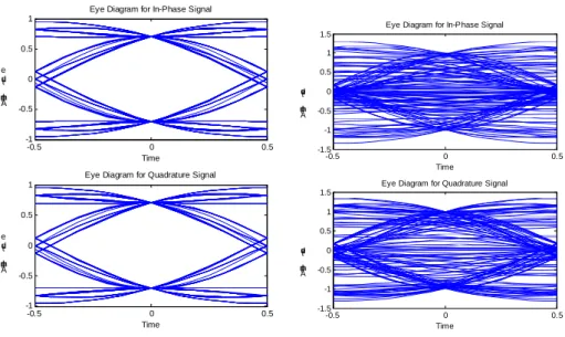
The intention of frequency synchronization is to estimate , the carrier frequency offset f between receiver and transmitter. is measured in ppm. With 2.4GHz carrier frequency, 1ppm f stands for 2.4kHz offset. According to the standard, the max carrier frequency offset (CFO) shall be confined to ±25ppm, that is, ±60kHz. Once CFO exceeds this limit, the constellation would rotate continuously, and cause the packet error rate (PER) remaining high even when SNR increases. Figure 4 shows the eye diagram.
-0.5 0 0.5 -1 -0.5 0 0.5 1 Time A mpli tu d e
Eye Diagram for In-Phase Signal
-0.5 0 0.5 -1 -0.5 0 0.5 1 Time A mpli tu d e
Eye Diagram for Quadrature Signal
-0.5 0 0.5 -1.5 -1 -0.5 0 0.5 1 1.5 Time A mpli tu d e
Eye Diagram for In-Phase Signal
-0.5 0 0.5 -1.5 -1 -0.5 0 0.5 1 1.5 Time A mpli tu d e
Eye Diagram for Quadrature Signal
Figure 4: Eye diagram of non-CFO(left) and with CFO(right)
Figure 5 depicts the Barker correlator output waveform under CFO = 25ppm. To emphasize the CFO impact, no AWGN is added in this experiment. From this figure, we can see that the real and imaginary parts for the received Barker sequence, although they have the expected sine and cosine-shape of envelops, are indeed twisted and non-smooth.
0 100 200 300 400 500 600 -20 -10 0 10 20 Real part 0 100 200 300 400 500 600 -20 -10 0 10 20 Imaginary part
Figure 5: Barker correlator output with CFO 25ppm.
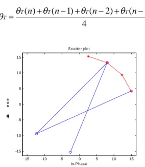
‘o’-shape markers point out the peaks and the dash-dot line shows their trajectory, in Fig. 6, we found that if all the peaks are mapping to the right side of y-axis relative to the origin, i.e., the ‘*’ marks in Fig. 6, then it is obvious that they would rotate the same phase as accumulated by the angle frequency 2f with one symbol time T. With this property, the carrier frequency offset
f
can be estimated with the data-directed differential decoding technique [11, 12, 13, 14, 15]. With differential decoding, the accumulated phase error is estimated as:
} ) 1 ( arg{ } ) ( arg{ ) ( DB n DB n1 T n C n F C n F
where arg{·} is an operator to get the angle inside {}. We then use “moving average” to eliminate the effect of AWGN. In principle, the longer the average window, the better the performance. In our system, four symbols are taken into average :
4 ) 3 ( ) 2 ( ) 1 ( ) ( T n T n T n T n T -15 -10 -5 0 5 10 15 -15 -10 -5 0 5 10 15 Q u a dr at ur e In-P hase S catter plot
Figure 6: Constellation and trajectory of Barker peak with CFO 25ppm
This symbol-based CFO estimation algorithm has its detection limit. With this method, the CFO could not exceed 90, otherwise the error would occur. This is because the DBPSK decision boundary is
90
. Thus, once the accumulated phase error exceeds this limit, CDB
would decode wrongly. So, the max tolerated CFO value in this design is ±104ppm.
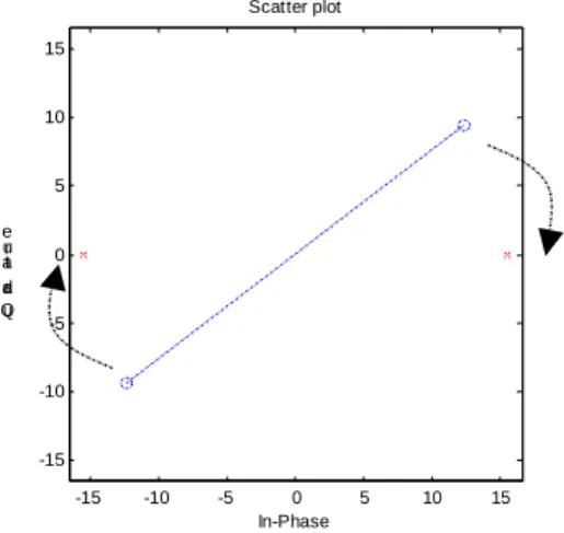
Phase synchronization
Once the CFO is estimated and starts to be compensated, the constellation would stop rotating and stop somewhere at p. The goal of phase synchronization is to remove the phase this
error p. If the Barker demodulator is non-coherent but differential, this phase error would not
affect the performance at all, and thus it is not necessary to remove it. However, coherent demodulator is used in our system; therefore, some efforts in this are needed. The phase error p
could be estimated with the Barker correlator output peak after CFO compensation started, namely,
Fnparg
The compensation of p is pretty simple, just rotating the constellation to the nearest prefect
constellation positions which in DBPSK are {+1, -1} as shown in Fig. 7.
-15 -10 -5 0 5 10 15 -15 -10 -5 0 5 10 15 Qu a dr at ur e In-Phase Scatter plot
Figure 7: Constellation of phase error and compensation method.
Timing synchronization
To get the highest input SNR, the ADC is hoped to sample at the eye open position where it has the maximum signal power. However, the initial sampling phase could be anywhere in the eye diagram, so timing synchronization is necessary.
The ADC has two kinds of clock sources: free running clock and phase lock loop (PLL) output clock. With free running clock, also known as non-synchronous sampling or fix sampling, clock frequency and phase are fixed. Once timing error estimated, the compensation would be performed with interpolator. With PLL output clock, also called synchronous sampling or dynamic sampling, it receives the timing error and adjusts its frequency and phase to compensate the error.
Figure 8 illustrates the block diagram of dynamic sampling. The clock source is PLL output. Different from the usual, the PLL here is implemented with all digital circuits, and is replaced by all digital delay lock loop (ADDLL) which has the same function and similar architecture as PLL. ADDLL would adjust the sampling clock frequency and phase directly once the timing error is estimated. It would not induce inter symbol interference (ISI) like interpolator and has better performance with less cost.
ADC Demod.
ADDLL Error Est.
clock
ADC Demod.
ADDLL Error Est.
clock
Figure 8: Block diagram of dynamic sampling.
We proposed the binary search algorithm by the comparison of the Barker peak power with different sampling phase. Once the timing synchronization starts, the Barker peak power of continuous four symbols is measured and marked as ‘M1’, then change the sampling clock phase and measure the power, ‘M2’. M1 and M2 were compared and next clock phase shift direction was determined in this way, then ‘M3’ is measured. After four times of measures and comparisons, best sampling clock phase was decided. Figure 9 illustrates the state diagram of binary search. M3 M4 M4 M1 M4 M3 M2 M4 M1>M2 M1<M2 M2>M4 M3<M2 M3<M1 M3<M2 M3>M1 M3>M2 M3>M4 M3<M1 M3>M2 M4<M1 M1>M4 M3>M2 M2<M4 M1<M4 M4>M1 0 1 2 3 4 5 6 7
Figure 9: State diagram of the binary search algorithm
To let timing synchronization work well at low SNR, early-late algorithm is used [11, 16, 17, 18]. For timing acquisition, Newton’s method is used to solve the desired timing. Figure 10 shows the S-curve of the proposed dynamic sampling algorithm.
1 2 3 4 5 6 7 8 9 10 -200 -150 -100 -50 0 50 100 150 200 S curve
Figure 10: S-curve of different sampling clock phase. The Newton’s method for timing acquisition is summarized as follows:
1. With random initial phase , measure 1 e(1) based on four consecutive Barker symbols.
2
1 2
.
3. Measure e(2) with four consecutive Barker symbols. 4. The slope 2 ) ( ) ( ) ( ' 1 2 1 e e e .
5. The best clock phase is then given by:
0 ) ( if 2 ) ( ' ) ( round 0 ) ( if 2 ) ( ' ) ( round ) ( ' ) ( round 1 1 1 2 1 1 1 2 1 1 1 3 e e e e e e e e
The proposed tracking algorithm is as follows.
1. After acquisition is completed, measure e(3) with eight consecutive symbols.
2. Shift right by 1 clock phase, 431, and measure e(4) with eight consecutive symbols.
3. Memorize the timing error of one clock phase, epcpe(4)e(3). 4. Shift the clock phase back, 541.
5. After 64 symbols counting from , measure the timing error 3 e(5).
6. Calculate the clock drift vector of 64 symbols
pcp cd e e e(5) (3)
and compensate(shift) one clock phase every
cd
22 64
samples.
With this proposed timing tracking algorithm, our receiver can predict the timing error and compensate it automatically without any help of MPDU data.
Figure 11: Amba interface MAC module.
As for the MAC design, we adopt the combination-logic design for the IEEE802.11 WLAN MAC protocol, and integrate it with the baseband processor. Since both the MAC circuit and the baseband circuit are implemented directly using the verilog language, a cell-level joint-simulation
can be readily performed in an on-line transceiving fashion, which largely ensures the workability of the resultant chip. To be more specific, two joint modules of MAC and baseband circuits exchange the sequence of RTS frame, CTS frame, DATA frame and ACK frame in our simulation.
As a consequence of taking the combination-logic design for the MAC, the gate counts can be largely reduced, the overall gate counts are about 21702, and its processing speed can be easily achieved 100Mbps. Furthermore, the user-variant customization function that is extra to the underlying MAC standard can be obtained through the realization of various on-chip configuration registers that are set by the host driver.
There are seven functional blocks in our MAC module: the PCMCIA host interface unit (PCMCIA HIU), Direct Memory Access and External SRAM Interface unit (DMA/ESI), Reception FIFO unit (RxFIFO), Transmission FIFO unit (TxFIFO), Reception Finite State Machine unit (RxFSM), Transmission Finite State Machine unit (TxFSM), and Timer unit (TIMER). The DMA/ESI handles data access to-and-from the PCMCIA HIU, RxFIFO, TxFIFO and the external SRAM. It arbitrates the data flows, which include (1) SRAM to Host through PCMCIA HIU, (2) Host to SRAM through PCMCIA HIU, (3) SRAM to TxFIFO, and (4) RxFIFO to SRAM. In our design, the latter two flows have higher priority than the former two. The external SRAM interface addresses up to 64K8 for temporary storage of the transmission frames and reception frames. By a flexible storage management scheme, an external SRAM of size 32K8 can momentarily accommodate, e.g., 16 received data/management frames and 1 transmitted data/management frame. These numbers can be flexibly adjusted by the host driver. For RxFIFO, the serial data received from baseband processor is translated into 32-bit parallel data, and then placed in the RxFIFO. The reception CRC32 check is also performed in this unit. For TxFIFO, the 32-bit parallel data from the TxFSM unit is translated into 32-bit serial data, and fed to the baseband processor. In this unit, the CRC32 is also computed and attached at the end of each transmission frame. In addition, in order to speed up the system response time, and to ease the burden of the host driver, all the Control frames and some of the time-critical Management frames (such as Beacon, Probe Response and ATIM) are handled by a combinational logic circuit in this unit. For example, upon a successful receipt of a data frame, the ACK control frame is
automatically returned without the intervening of the host driver. The RxFSM determines the after-processing of the received frames. For example, if the received frame is a data or management frame, then it is transferred and stored at the external SRAM. In case the received frame lies in the categories of RTS, CTS or ACK, then a respective indication is forwarded to the TxFSM. The TxFSM implements the DFW CSMA/CA. It also maintains the retransmission count, where the retransmission limit is set by the host driver at the initialization stage. The TIMER unit controls the various time counts for the MAC module, e.g., the backoff timer, IFS timer and the time-out counter. Since the backoff timer, IFS timer and time-out counter will never be launched at the same time, they can share the same counter circuitry so that a little reduction of the gate counts is rendered.
四、參考文獻
[1] IEEE Std. 802.11, Wireless LAN Medium Access Control (MAC) and Physical Layer (PHY) Specifications, 1999 edition.
[2] IEEE Std. 802.11b, Higher-Speed Physical Layer Extension in the 2.4 GHz Band, 1999. [3] IEEE Std 802.11a, High-Speed Physical Layer in the 5GHz Band, 1999.
[4] F.-S. Lin, Design and Implementation of IEEE802.11 MAC Controller : Transmitter Part, Master Thesis, Institute of Communications Engineering, National Chiao Tung University, Hsin Chu, Taiwan, R.O.C., June 1999.
[5] M.-T. Hong, Design and Implementation of IEEE802.11 MAC Controller, Master Thesis, Institute of Communications Engineering, National Chiao Tung University, Hsin Chu, Taiwan, R.O.C., June 1999.
[6] S.-P. Huang, Design and Implementation of High Speed IEEE802.11 MAC Controller, Master Thesis, Institute of Communications Engineering, National Chiao Tung University, Hsin Chu, Taiwan, R.O.C., June 2000.
[7] PCMCIA, PCMCIA PC Card Standard Release 2.01, Section 4: Card Interface, 1992.
[8] T.-B. Pei and C. Zukowski, “High-speed parallel CRC circuits in VLSI,” IEEE Trans. on Commun., vol. 40, no. 4, pp. 653-657, April 1992.
[9] Ren-Zong Li, Shang-Pin Huang, Fu-Shung Lin, Ming-Tsung Hong and Po-Ning Chen, “A combination logic design of high speed IEEE 802.11 MAC controller,” Journal of the Chinese Institute of Engineers (JCIE), vol. 26, no. 2, pp. 255-258, March 2003.
[10] Van Nee, R. D. J., “OFDM codes for peak-to-average power reduction and error correction”, IEEE Global Telecommunications Conference, pp.740-744, 1996.
[11] Umberto Mengali and Aldo N. D’Andrea, Synchronization Techniques for Digital Receivers, Plenum Press, 1997.
[12] M. P. Fitz, “Planar filtered techniques for burst mode carrier synchronization,” GLOBECOM’91, paper 12.1., Phoenix, Arizona, Dec. 2-5, 1991.
[13] M. P. Fitz, “Further results in the fast estimation of a single frequency,” IEEE Trans. Commun., COM-42, pp. 862-864, March 1994.
[14] M. Luise and R. Reggiannini, “Carrier frequency recovery in all-digital modems for burst-mode transmissions,” IEEE Trans. Commun., COM-43, pp. 1169-1178, 1995.
[15] D. G. Messerschmitt, “Frequency detectors for PLL acquisition in timing and carrier recovery,” IEEE Trans. Commun., COM-27, pp. 1288-1295, Sept. 1979.
[16] W. C. Lindsey and M.K. Simon, Telecommunication Systems Engineering, Englewood Cliffs , NJ , prentice Hall , 1972.
[17] K. H. Mueller and M. Mueller, “Timing recovery in digital synchronous data receivers,” IEEE Trans. Commun., COM-24, pp. 516-531, May 1976.
[18] F. M. Gardner, “A BPSK/QPSK timing-error detector for sampled receivers,” IEEE Trans. Commun., COM-34, pp. 423-429, May 1986.
五、研究成果自評
在 此 三 年 的 研 究 中,我 們 於 第 一 年 完 成 高 速 無 線 數 據 存 取 控 制 與 基 頻 收 發 各 積 體 電 路 子 模 組 的 界 面 規 劃 與 設 計 , 以 及 ISM 頻帶的基頻調變技術以及通道的分析和 評估。 第 二 年 的 計 畫 則 著 重 在 核 心 技 術 的 發 展 與 系 統 整 合 ; 於 基 頻 方 面 , 我 們 設計了一個互補式編碼調變的 11Mbps 無線區域網路基頻處理晶片,並利用 SPW 做系統性 能驗證及評估,最後再以 Verilog 做實體層的系統模擬。為了使介質存取控制器與 基 頻 處 理 器 能 整 合 於 單 一 晶 片 上,介質存取控制器以 標準單元式積體電路為架構,並以 ARM 為控制核心進行設計,在此架構下我 們 用 純 組 合 邏 輯 設 計 達 成 IEEE 802.11 所 規 範 的 具 碰 撞 避 免 功 能 的 分 立 架 構 無 線 載 波 偵 測 多 重 存 取,同 時 也 用 組 合 邏 輯 處 理 需 及 時 處 理 的 控 制 框 架 與 管 理 框 架。在 基 頻 與 介 質 存 取 模 組 的 介 面 上,採 用 高 速 FI FO 的 架 構 , 在 製 程 的 模 擬 上 確 實 達 到 100Mbps 以 上 的 傳 輸 速 度 。 在第三 年的計畫,我們提出並實作一個新的 CCK 基頻同步演算法,同時為驗證我們所設計的基頻 與介質存取模組之單晶片整合的可行性,我們除了進行系統整合模擬,並於兩套 ARM Evaluation Board 與其上的 FPGA 上完成互傳測試。 究 此 , 本 研 究 確 已 達 成 原 定 計 畫 目 標 , 我 們 所 開 發 出 來 的 原 始 設 計 碼 具 有 相 當 的 應 用 價 值 。附錄一: 可供推廣之研發成果資料表
□ 可申請專利 ▓ 可技術移轉 日期:92 年 8 月 29 日國科會補助計畫
計畫名稱:高 速 無 線 數 據 存 取 控 制 與 基 頻 收 發 積 體 電 路 模 組 整 合 IP 之 設 計 及 實 作 計畫主持人:陳伯寧教授 計畫編號:NSC 89(90, 91)-2218-E-009-052(004, 003)- 學門領域:3C 整合科技技術/創作名稱
AMBA Interfaced IEEE 802.11a/b MAC Controller發明人/創作人
陳伯寧中文:在本計畫的執行過程中,我們將本實驗室所開發適用於 IEEE 802.11a/b/g 之 Combinational-logic-based MAC Controller Module,改為 AMBA Interface 並 Port 到 ARM Evaluation Board, 以之為平台進行整合互傳 MPEG 資料測試。此模組應可作為獨立之 IP 供推廣。
技術說明
英文:In this project, we have refined our IEEE 802.11 a/b/g PCMCIA-interfaced Combinational-logic MAC Controller Module to AMBA interface, and ported this Verilog code to ARM Evaluation Board for on-line transceiving testing of MPEG data. This module can be an independent IP for technology transfer.
可利用之產業
及
可開發之產品
無線通訊晶片廠商與系統整合廠商
技術特點
A combinational-logic design, although less flexible, hasthe advantage of cost-effectiveness in processing speed.
推廣及運用的價值
A combinational-logic design, although less flexible, hasthe advantage of cost-effectiveness in processing speed. ※ 1.每項研發成果請填寫一式二份,一份隨成果報告送繳本會,一份送 貴單位
研發成果推廣單位(如技術移轉中心)。
※ 2.本項研發成果若尚未申請專利,請勿揭露可申請專利之主要內容。
□ 可申請專利 ▓ 可技術移轉 日期:92 年 8 月 29 日
國科會補助計畫
計畫名稱:高 速 無 線 數 據 存 取 控 制 與 基 頻 收 發 積 體 電 路 模 組 整 合 IP 之 設 計 及 實 作 計畫主持人:陳伯寧教授 計畫編號:NSC 89(90, 91)-2218-E-009-052(004, 003)- 學門領域:3C 整合科技技術/創作名稱
Dynamic sampling for IEEE 802.11a/b Baseband Processor發明人/創作人
李鎮宜中文:在本計畫的執行過程中,我們將本實驗室所開發適用於 SOC 之 ADDLL/ADPLL 擴 展 為 IEEE 802.11a/b/g Timing synchronization 並 Port 到 Matlab Platform,以之為平台進行整 合測試。此模組應可作為獨立之 IP 供推廣。
技術說明
英文:In this project, we have refined our IEEE 802.11 a/b/g ADDLL/ADPLL-based dynamic sampling, and ported this technique to Matlab platform/Verilog and to verify its performance. This module can be an independent IP for technology transfer.
可利用之產業
及
可開發之產品
無線通訊晶片廠商技術特點
An all digital-based approach of DLL/PLL for dynamic sampling, has the advantages of performance and cost-effectiveness in system integration.
推廣及運用的價值
An all digital-based approach of DLL/PLL for dynamic sampling, has the advantages of performance and cost-effectiveness in system integration.
※ 1.每項研發成果請填寫一式二份,一份隨成果報告送繳本會,一份送 貴單位
研發成果推廣單位(如技術移轉中心)。
※ 2.本項研發成果若尚未申請專利,請勿揭露可申請專利之主要內容。