國
立
交
通
大
學
材料科學與工程學系
博
士
論
文
奈米介孔材料之合成、結構及其氣體感測性質
之研究
Fabrication, Structure and Gas Sensing Applications of
Mesostructured Materials
研 究 生:劉厥揚
指導教授:陳家富 教授
呂志鵬 教授
奈米介孔材料之合成、結構、及其氣體感測性質之研究
研究生:劉厥揚 指導教授:陳家富 博士
呂志鵬 博士
國立交通大學
材料科學與工程研究所
摘 要
近年來,隨著工業的進展及環保意識的重視,各種廢氣量日益增加,對於有毒氣體 如CO, CO2, SO2, NO2等外在環境的控制亦趨重要。它們對人體有害,同時也對環境造成 嚴重的傷害。因此,偵測汙染源並提出預警變的更顯重要。為了改善傳統氣體感測器之 昂貴、笨重與偵測耗時等缺點,近年來已有許多研發專注於新型氣體感測器之上。 本研究利用模版複印法製備三種新型態的奈米孔洞氣體感測器。在多孔的二氧化矽 模板上分別製備p型半導體的多孔碳及多孔氧化鈷感測材料 ; 另外,利用多孔碳為模板 製備n型半導體的多孔氧化鋅感測材料。初製備的此三種奈米孔洞材料均具有均勻尺寸 與多孔性,利用X光繞射(XRD)光譜對不同的樣品做相鑑定;利用掃描式(SEM)及穿透式 電子顯微鏡 (TEM)量測材料的結晶結構和顯微結構;利用氮氣吸脫附分析儀(BET)分析 材料的表面積及孔洞的尺寸。並研究奈米孔洞材料的結構、表面形態對於ㄧ氧化碳感測 特性的影響。由實驗結果得之,此三種孔洞感測材料在相當低濃度(10-100 ppm)的ㄧ氧 化碳環境下均具有良好的感應能力,其中具有單晶結構的多孔氧化鋅感測材料具有 51.7%的敏感度,並提出此新穎氣體感測器之可能的感測機制。 另外,為了減少能量的消耗,本研究也結合微機電技術設計並製作新型微型薄膜氣 體感測器。感測器以矽為基材,並包括了加熱器、絕緣層、電極、感測層等結構,而感 測材料則是在室溫下利用電泳方式排列沉積。在電泳過程中感測材料因為受到電場極化 作用下聚集並沿著電場方向排列,最後成功的吸附在電極上。由實驗結果得之,多孔材 料的規則排列的結構提供更多的活性反應面積使得多孔氧化鋅感測材料在70 ppm CO下有60.0%的敏感度且反應時間約為90秒。此種新穎的氣體感測器具有高靈敏度、快速的 反應時間及良好的可逆性等特性,為一新穎且簡易之氣體感測器。
Fabrication, Structural and Gas Sensing Applications of Mesostructured
Materials
Student:Chueh-Yang Liu Advisor:Dr. Chia-Fu Chen
Dr. Jih-Perng Leu
Institute of Materials Science and Engineering
National Chiao-Tung University
Abstract
Recently, environmental protection has gained attention as a result of industrial development and an increase in the emission of various kinds of exhaust gases. Noxious gases such as CO, CO2, SO2, and NO2 are presented in the atmosphere. They are highly toxic for the human body and also cause indirect harm to the environment. Traditional gas sensors that have been used thus far are expensive, heavy, and prone to delay; in order to overcome these problems, many studies have focused on developing gas sensors.
In this study, three novel nanoporous gas sensors were synthesized by using the template replication method. P-type semiconducting sensors for example mesostructured carbon and mesostructured cobalt oxide were synthesized using a porous SiO2 template. Further, an n-type semiconducting porous ZnO sensor was synthesized using porous carbon as a template. The prepared mesostructured materials were highly ordered porous atructure with uniform particle sizes. Powder x-ray diffraction (XRD) spectra of the different mesostructured materials confirm the phase of these materials. The crystal structure and microstructure of the mesostructured materials were observed by scanning electron microscopy (SEM) and transmission electron microscopy (TEM). The surface areas and pore
-
size distributions of themesostructured materials were analyzed by N2 adsorption-desorption isotherms. Structural and morphological studies were carried out in order to investigate the influence of these materials on the sensing properties of sensors synthesized using mesostructured materials. All of the sensing materials have good sensitivity for low CO concentrations (10
–
100 ppm). Among the porous sensing materials, porous ZnO had a sensitivity of 51.7%. The sensing-mechanism of these novel gas sensors was reviewed.In order to reduce the power consumption in sensors, in this study, we have designed and developed a system for measuring energy consumption on the microscopic scale. Sensors were fabricated on silicon substrates using micro electromechanical systems (MEMS) technologies and compatible with integrated circuit (IC) process. The layers in the device include a micro-heater, an isolator, electrodes, and a sensing film. The sensing materials were aligned and immobilized between electrodes by using the dielectrophoresis process, which is known to be a convenient method for the manipulation of dielectric substances in a liquid. Experimental results showed that the regular aligned structure of these mesostructured materials provide number of active areas on the sensor; porous ZnO had a sensitivity of 60.0% and had a fast response time of 90 s. These mesostructured gas sensors have been developed in this study with high sensitivity, good response properties and good repeatability. Moreover, the preparation process of the mesostructured sensor was a simple method.
誌謝
四年半,一個說長不長說短也不短的時間,我完成了我的博士生涯。寫此篇誌謝的 當下中,心中百感交集,有喜悅也有不捨。當順利完成此本論文的同時,心中滿懷喜悅 與感激,喜悅的是順利完成博士論文;不捨的則是要離開美麗的交大校園跟一起打拼的 夥伴們。首先要感謝我的指導教授-陳家富老師-在專業知識及相關領域上的細心指導與 解惑及其他方面的訓練與指導,使學生獲益不少。此外,也很感謝我的另一位指導教授 -呂志鵬老師-在實驗方面給予許多的建議。另外,感謝暨南大學 孫台平院長、交通大 學材料系 陳三元教授、明新科大化工系 陳密教授於口試期間的建議與指導,使學生的 論文更加充實,在此致上最誠摯的謝意。 研究期間,感謝實驗室的成員-士塵學長、鴻鈞學長、光中學長、建仲學長、建銘 學長、振航學長、騰凱同學及琮琦、瑞豪、方慈、宜輝、家駿等學弟及明道大學政宜、 昱顯、朝俊等學弟的的鼎力幫忙,使我在博士班的生涯中更多采多姿。另外,感謝目前 在高應大任教的弘穎學長在實驗方面的經驗傳授與指教,使我實驗能更順利完成。還有 德銘學長、詠煌、建民、世緯、伸鈜、又維、小麥、賀昌、牧龍、昱涵、均元、少農、 宏偉、文碩、崇榮、冠名、志遠等學弟及志欣、維齡、小蔡等學妹在實驗上的幫忙與鼓 勵。特別感謝交大材料的克遙、蕙馨跟麗娟姐在行政上的大力幫忙。由於要感謝的人太 多,不及一一備載,望請海涵。 最後,僅以此篇論文至給我最愛的家人及所有關心我的人,感謝你們在背後無怨無 悔的支持與鼓勵,謝謝。Contents
中文摘要 ...i Abstract ...iv Acknowledge...vi Contents ...vii Table Caption...ix Figure Caption ... x Chapter 1 Introduction... 1 1.1 Background... 1 1.2 Motivation ... 3Chapter 2 Mesoporous Materials: Literature Review... 5
Chapter 3 Functionals of Semiconductor Metal Oxide Gas Sensor ... 13
3.1 Physisorption and Chemisorption... 14
3.2 Charge Tranfer Model (CTM) ... 15
3.3 Depletion Layers Effect... 17
3.4 Necked-controlled and Grain Boundary Effect ... 18
3.5 Scottky Contact ... 21
3.6 Oxygen Vacancy ... 23
Chapter 4 Experimental Methods... 25
4.1 Synthesis of Mesoporou Materials ... 25
4.1.1 Synthesis of mesoporous silica template... 25
4.1.2 Synthesis of mesoporous carbon ... 25
4.1.3 Synthesis of mesoporous metal oxide materials... 26
4.2 Fabrication of mesostructured sensing device... 27
4.2.2 Fabrication of thin-film sensors... 27 4.3 Characterization... 31 4.3.1 XRD... 31 4.3.2 FE-SEM... 31 4.3.3 TEM... 31 4.3.4 DTA/TGA... 31 4.3.5 XPS... 31 4.4 Gas-sensing measurement ... 32
Chapter 5 Result and discussion... 34
5.1 Mesoporous silica template ... 34
5.1.1 Synthesis of SBA-15 at different temperatures ... 34
5.1.2 Synthesis of SBA-15 at low acid concentrations ... 49
5.1.3 Two step desorption isotherm of SBA-15 ... 54
5.2 Mesostructured cobalt oxide materials... 55
5.3 Mesostructured carbon materials... 79
5.4 Synthesis of mesostructured ZnO materials ... 97
5.5 Mesostrtured-based micro sensors ... 104
5.5.1 Overview of the micro-sensor ... 105
5.5.2 Gas-sensing for DEP-trapped mesostructured materials ... 107
5.6 Tunable interconnectivity of mesostructured materials on sensing performance ... 121
5.7 The new mechanism of mesostructured-based sensors ... 124
Chapter 6 Conclusions... 127
Table Captions
Table 1.1 Typical deposition techniques used for preparation of gas-sensitive materials based on semiconductors……….………...2 Table 2.1 Pore-size definition of the porous materials ……….………... ..5 Table 5.1 Device specification for mesostructured materials………. …….116
Figure Captions
Figure 1.1 The sensor material is deposited on the interdigitated electrode ...4
Figure 2.1 Two possible pathways for the LCT mechanism... 6
Figure 2.2 Assembly of silicate rods ...7
Figure 2.3 Puckering of silicate layers in the direction ...7
Figure 2.4 Curvature induced by charge density matcging. The arrow indicates the reaction coordinate ...………8
Figure 2.5 Folding of silicate sheets around intercalated surfactant moloecules. (a) Ion exchange, (b) calcinate... 8
Figure 2.6 Formation of a silicatropic liquid crystal phase... 9
Figure 2.7 The illustrations of M41S materials: (a) MCM-41, (b) MCM-48, and (c) MCM-50 .. ... 10
Figure 2.8 The schematic diagram of SBA-15 synthesizes with triblock copolymer... 11
Figure 3.1 The thermal desorption spectra (TDS) of molecular oxygen on ZnO. Curve C is the first heat treatment ... 15
Figure 3.2 The space charge at the surface of an n-type semiconductor (left) and of a p-type semiconductor (right) due to the adsorption of an electron acceptor. (a) Distribution of the charge carrier. (b) Band deflection at the semiconductor surface. (c) Charge carrier concentration in the conductor resp. valence band. EC: edge of the conduction band, EV: edge of the valence band, EF: Fermi level, ED: donor level, EA: acceptor level, EI: intrinsic level, nb: concentration of electrons in the bulk, pb: concentration of holes in the bulk. ... 16 Figure 3.3 Charge carrier concentration n and conduction band EC for a contact position of grain boundaries for a grain with a Debye-length (LD) less than half grain size on the left side and a grain with a Debye-length more than half grain size on the right
side. ... 18
Figure 3.4 Surface space charge layer and electron transport between grain and target gases. (a) Grain boundaries, (b) Necked. E: Potential energy of electrons. ... 19
Figure 3.5 Assumed electron density profiles at the cross section of a neck. ... 20
Figure 3.6 Schematic diagram of grain size effect of nanoparticles. ... 20
Figure 3.7 (a) Energy-band diagram of metal-oxide-n-type semiconductor jubction: (1) Before contact, (2) After contact and thermodymanic equilibrium is attained, in the presence of a gap (or an insulating dielectric) of thickness d, (3) When d is comparable to interatomic distance, and (4) in the limit d=0 (metal-semiconductoe junction) ... 22
Figure 4.1 Schematic of the alumina substrates with the intergiditated electrodes... 27
Figure 4.2 The fabrication schematic diagram of the micro sensor device... 28
Figure 4.3 Schematic diagram of the DEP system.. ... 29
Figure 4.4 The OM images (a) before the DEP immobilized; (b) after the DEP immobilized of the mesostructured metal oxide samples... 30
Figure 4.5 The diagram of the mesostructured materials testing chamber... 32
Figure 5.1 XRD patterns of as-synthesized SBA-15 template.. ... 35
Figure 5.2 The SEM image of as-synthesized SBA-15 template.. ... 35
Figure 5.3 (a) The nitrogen isotherms of as-synthesized SBA-15 and (b) the corresponding pore size distribution.. ... 36
Figure 5.4 The XRD patterns of SBA-15 synthesized at 40, 60 and 100°C.. ... 38
Figure 5.5 (a) Nitrogen adsorption-desorption isotherms and (b) pore size distribution of SBA-15 synthesized at 40, 60, and 100°C.. ... 39
Figure 5.6 The SEM images of SBA-15 synthesized at different temperature. (a) 40°C, (b) 60°C, and (c) 100°C... 40 Figure 5.7 The TEM micrographs of SBA-15 synthesized at different aging temperatures (a)
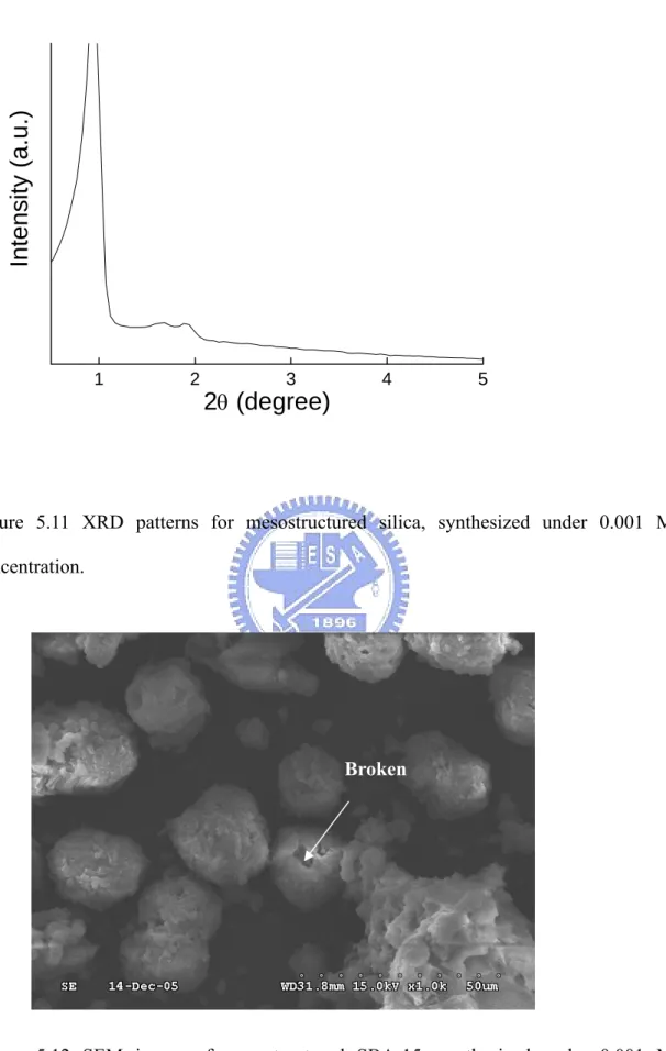
40°C, (b) 60°C, and (c) 100°C.. ... 44 Figure 5.8 Schematic representation of micelle dehydration upon temperature.. ... 45 Figure 5.9 Phase diagram of P123, EO20PO70EO20... 45 Figure 5.10 Schematic representation of SBA-15 synthesized (a) between 40 and 60 °C showing micropores and no connection between mesopores, (b) around 100°C showing micropores and connection between mesopores.. ... 48 Figure 5.11 The XRD patterns for the mesostructured silica synthesized under 0.001 M acid concentrations.. ... 50 Figure 5.12 The SEM image of mesostructured SBA-15 synthesized under 0.001 M acid concentration... 50 Figure 5.13 Nitrogen adsorption-desorption isotherm of “plugged” mespores, comprising both
open and blocked mesopores, intrawall micropores, and microporous silica nanocapsules ... 53 Figure 5.14 Thermal decompositions plot of the cobalt-silica composite... 56 Figure 5.15 (a) XRD patterns of samples with cobalt oxide in SBA-15 at different aging temperatures, and (b) XRD patterns of cobalt oxideheated at 250°C with varying times.. ... 57 Figure 5.16 XRD patterns of the specimens after decomposing Co(NO3)2‧6H2O without the
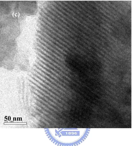
presence of silica template.. ... 59 Figure 5.17 SEM images of mesostructured Co3O4 materials heated at 250°C with varying times: (a) 10 min, (b) 30 min, (c) 60 min, (d) 180 min, and (e) 360 min, respectively. Typical bright-field TEM image of the mesostructured Co3O4 materials in (f), inset is the corresponding selected areas electron diffraction; (g) shows a corresponding HRTEM image of (f).. ... 63 Figure 5.18 XPS measurement for (a) Co2p, and (b) O1s core levels for mesostructured cobalt
Figure 5.19 (a) Nitrogen adsorption-desorption isotherms measured at 77 K and (b) corresponding pore size distributions of the mesostructured cobalt oxide materials... ... 66 Figure 5.20 The XRD patterns at (a) low-angle, (b) wide-angle regions of the mesostructured
cobalt oxide materials with the templates prepared from different temperatures: (I) 40°C, (II) 60°C, and (c) 100°C.. ... 69 Figure 5.21 Effect of size variation in 2D hexagonal parent silica on the preparation cobalt oxide. TEM images of preparation cobalt oxide at different crystallization temperatures: (a) 40°C, (b) 60°C, and (c) 100°C... 71 Figure 5.22 Nitrogen adsorption-desorption isotherms of cobalt oxideprepared from SBA-15 templates with different crystallization temperatures: (I) 40°C, (II) 60°C, and (III) 100°C ... 71 Figure 5.23 Schematic diagram of preparing metal oxide arrays... 73 Figure 5.24 Sensor response and recovery times of mesostructured materials with the applied
voltages modulated from 1 V to 10 V... 74 Figure 5.25 Sensor response of mesostructured cobalt oxide materials to 20 ppm CO at different working temperatures.. ... 76 Figure 5.26 The SEM images of mesostructured cobalt oxide sensing materials printed on the
alumina substrate... 76 Figure 5.27 Dynamic response of mesostructured cobalt oxide materials to different
concentrations of CO in synthetic air at 200°C... 77 Figure 5.28 Sensor response of mesostructured cobalt oxide materials to different
concentrations of CO in synthetic air... 77 Figure 5.29 The low-angle XRD patterns of mesostructured carbon synthesized from SBA-15
silicas at different carbonization temperatures: (i) 600°C, (ii) 700°C, (iii) 900°C, and (iv) 1000°C... 80
Figure 5.30 Representative SEM image for mesostructured carbon at different carbonization temperatures: (a) 600°C, (b) 700°C, (c) 900°C, and (d) 1000°C... 82 Figure 5.31 TEM images of the mesostructured carbon after carbonization treatment at 900°C..
... 84 Figure 5.32 The nitrogen adsorption-desorption isotherms of mesostructured carbon at different carbonization temperatures: (i) 600°C, (ii) 700°C, (iii) 900°C, and (iv) 1000°C.. ... 84 Figure 5.33 XPS spectra of mesostructured carbon carbonized at different temperatures: (a) 600°C, (b) 700°C, (c) 900°C, and (d) 1000°C.. ... 85 Figure 5.34 (a) Nitrogen adsorption-desorption isotherm and (b) pore size distribution curves of mesostructured carbon from various SBA-15 templates: (i) 40°C, (ii) 60°C, and (c) 100°C... 89 Figure 5.35 The low-angle XRD patterns of the mesostructured carbon synthesized from various silica templates: (i) 40°C, (ii)60°C, and (iii) 100°C... 90 Figure 5.36 Representative SEM images of the mesostructured carbon materials synthesized at various SBA-15 templates: (i) 40°C, (ii) 60°C, and (iii) 100°C.. ... 90 Figure 5.37 Representative TEM images of the mesostructured carbon materials synthesized at various SBA-15 templates: (i) 40°C, (ii) 60°C, and (iii) 100°C.. ... 92 Figure 5.38 The SEM images of mesostructured carbon sensing materials printed on the alumina substrate... 95 Figure 5.39 Sensor responses of mesostructured cobalt oxide materials to different
concentrations of CO in synthetic air... 95 Figure 5.40 An energy band diagram of the Schottky barrier formed at interface between metal and p-type mesostructured carbon. EF: Fermi level; EC: conduction band; EV.. ... 96 Figure 5.41 Concentrations dependence of the mesostructured carbon gas sensor response.... 96
Figure 5.42 (a) low angle XRD patterns and (b) wide angle XRD patterns of the mesostructured ZnO... 98 Figure 5.43 SEM image of the mesostructured ZnO... 99 Figure 5.44 (a) TEM image of mesostructured ZnO materials, as a replica of mesostructured
carbon template. (b) HRTEM micrograph of the crystalline framework of mesostructured ZnO... 99 Figure 5.45 XPS spectra of (a) Zn 2p spectra, and (b) O 1s spectra of the mesostructured ZnO..
... 101 Figure 5.46 Variation of sensing response of mesostructured ZnO sensor with temperature at
20 ppm CO.. ... 104 Figure 5.47 Sensing response of mesostructured ZnO sensor determined with several CO concentrations.. ... 104 Figure 5.48 Schematic design of a micro sensor device with the micro-hotplate membrane..106 Figure 5.49 The top-view diagram of the micro sensor electrode... 106 Figure 5.50 (a) low-magnification SEM images and (b) high-magnification SEM images of DEP-trapped mesostructured cobalt oxide... 108 Figure 5.51 Dynamic sensor response of DEP-trapped mesostructured cobalt oxide sensor measured with various CO concentrations... 110 Figure 5.52 Switching response of the DEP-trapped mesostructured cobalt oxide exposed to 50 ppm CO. ... 110 Figure 5.53 Linear sensor response of the DEP-trapped mesostructured cobalt oxide at various
CO concentrations... 111 Figure 5.54 (a) low-magnification SEM images and (b) high-magnification SEM images of DEP-trapped mesostructured ZnO.. ... 113
ppm CO gas, and (b) sensing response of mesostructured ZnO sensor determined with several CO concentrations.. ... 115 Figure 5.56 The SEM images of (a) low magnification and (b) high magnification of the DEP-trapped mesostructured carbon.. ... 119 Figure 5.57 (a) Response of the mesostructured carbon sensor measured with various CO concentrations and (b) Switch response of the mesostructured carbon sensor exposed to 30 ppm CO gas.. ... 120 Figure 5.58 The sensor resistance of mesostructured cobalt oxide materials at different crystallization temperatures: (I) 40°C, and (II) 100°C... 122 Figure 5.59 Relationship between the sensitivity of mesostructured cobalt oxide sensor at different crystallization temperatures: (I) 40°C, and (II) 100°C... 122 Figure 5.60 The diagram showing the gas accessibility for mesostructured materials.. ... 126
Chapter 1 Introduction
1.1 Background
The increase in air pollution-as evidenced by acid rain, increase in particulate matter, the disappearance of the ozone shield, and the appearance of greenhouse effect-has thus far been the result of development in industry and technology. Such developments are an inconvenience and detriment to all human life. The gases involved include CO, CO2, NOx, SOx, hydrocarbons, and hydrogen; these pollution gases have been cited as the main causes of “global warming” and “greenhouse effects” [1]. In light of these developments, various techniques have been widely used in the accurate analysis and detection of these gases. The installation of these conventional instruments is costly, and they require not only a sampling system and regular maintenance but also the continuous monitoring of most gases. To fulfill these demands, a device has been developed with an eye to safety, economy, pollution control, and the logistics of industrial processes. The majority of these devices involve the application of surface or bulk chemicals to determine the physical properties of materials; for this reason, many of them are called chemical sensors [2-5]. In general, there are three kinds of gas sensor categories: (1) solid electrolyte gas sensors, (2) catalytic combustion gas sensors, and (3) semiconductor gas sensors. They possess certain characteristics-such as low cost, quick sensor response, prompt recovery times, good mechanical strength, and long lifetime-that make them as attractive as semiconductor gas sensors to commercial sensor users [6].
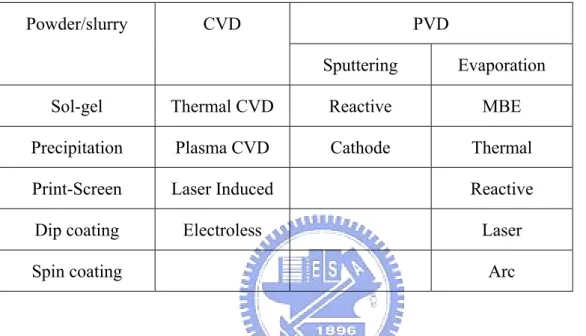
In the last decade, several researchers and industries have developed optimal gas sensors, with the goal of determining a parameter to which optimized sensors can be manufactured and set to monitor, vis-à-vis different substances in different environmental conditions [7]. The synthesis and deposition of the sensing layer is obviously the most crucial part of preparing of gas sensors, and there are three main groups thereof: powder/slurry deposition, chemical
vapor deposition (CVD) and physical vapor deposition (PVD). The preparation methods for sensing films are listed in Table 1 [7, 8].
Table 1.1 Typical deposition techniques used for preparation of gas-sensitive materials based on semiconductors.
PVD Powder/slurry CVD
Sputtering Evaporation Sol-gel Thermal CVD Reactive MBE Precipitation Plasma CVD Cathode Thermal Print-Screen Laser Induced Reactive
Dip coating Electroless Laser
Spin coating Arc
The traditional sensing material is usually deposited as a polycrystalline film or layer on a substrate with integrated electrodes and a heater (Figure 1.1) [9]. Extensive scientific research has focused on the optimization of semiconducting sensors with respect to their sensitivity, response rate, gas selectivity, and economic efficiency [10–15]. It is apparent that the physics and chemistry of semiconducting sensing equipment is complex and not yet understood. Although several principles vis-à-vis semiconducting sensing equipment have been identified, it has often been difficult to improve sensing performance. The most important properties of semiconducting sensing materials equipment are their sensitivity, operating temperature, selectivity, and long-term stability. On the other hand, the optimal sensing equipment should provide strong and noise-free changes in conductance upon changes in target gas concentration, as well as shorter response times and a reliable lifecycle. Finally, their energy consumption should be minimal.
1.2 Motivation
Apart from being applicable in a more universal fashion, the structure replication method bears another important advantage over the use of amphiphiles as structure directors, as well as over regular sol-gel synthesis lacking structure directors. In general, rigid matrices can withstand high temperatures during the formation of the desired metal oxides inside their pore systems. Serving as a rigid skeleton, a solid-state template allows for temperatures of several hundred degrees, without a loss of periodic structure. Thus, higher degrees of crystallinity and larger single-crystalline domains are possible. The concept of using structure directors or rigid structure matrices for the synthesis of mesoporous metal oxide gas sensors offers a number of substantial advantages over conventional synthesis methods. Mesoporosity plays a vital role in the application of semiconducting metal oxides as gas sensors. Apart from exhibiting high sensitivities due to their large specific surface areas, sensors with well-defined porosity offer powerful opportunities with respect to selectivity, self-diagnosis, low operation temperatures, and long-term stability. With respect to many key structural parameters—such as grain size, grain interconnectivity, pore size, and pore architecture—conventional synthesis methods do not allow efficient and individual control. New synthesis concepts of structure direction and structure replication provide new opportunities to create materials with defined mesoporosity and improved gas-sensing properties. The first objective of this study was to synthesize and characterize mesostructured materials—such as mesostructured carbon, zinc oxide, and cobalt oxide—by using a hard-template route and the application of gas-sensing measurement. For this purpose, mesostructured sensing materials were pasted on traditional alumina substrates, using the print-screen method.
The other objective of this study was to discover a micro-sensing device that used SOI technology and was fully CMOS-compatible. The mesostructured sensing materials were immobilized by the dielectrophoresis (DEP) process, while characterization of the structural and textural properties was carried out with X-ray diffraction (XRD), scanning electron
microscopy (SEM), yransmission electron microscopy (TEM), X-ray photoelectron spectroscopy (XPS), and a surface-areas analyzer. The sensing mechanisms of the mesostructured materials will also be discussed.
Chapter 2 Mesoporous Materials: Literature Review
In 1992, a novel family of molecular sieves called M41S was launched by Mobil Corporation [16]. The pore size of these mesoporous materials were 15–100Å. These materials attracted interest due to their large pore size (>1200 m2 g–1) and tunable pore sizes. The M41S materials also provide a new approach in materials synthesis, supplanting the use of single molecules (zeolite) as templating structure-directing agents. In general, inorganic solids containing pores whose diameter range from 20 to 500 Å are considered mesoporous materials, according to IUPAC definition. Examples of mesoporous materials such as M41S, aerogels, and pillared layered structures as listed in Table 2.1.
Table 2.1. Pore size definition of the porous materials
Pore size Definition Examples
Macroporous (> 500 Å) Glasses Mesoporous ( 20-500 Å) Aerogels, M41S Microporous ( < 20 Å) Zeolites, Actived Carbon
On the most fundamental level, the formation of mesoporous materials from inorganic precursors and organic surfactants occurs in the presence of surfactants, in a solution from solubilized inorganic precursors. Surfactants contain a hydrophilic head group and a long hydrophobic tail group within the same molecule, and they will self-organize so as to minimize contact between the incompatible ends. The type of interaction between the surfactant and the inorganic precursor is seen as a significant difference among the various synthesis routes, the formation models, and the resulting classes of mesoporous materials [17]. A liquid crystal templating (LCT) mechanism has been proposed, based on the similarity (i.e.,
lyotropic phase) between liquid crystalline surfactant assemblies and M41S [18]. Common traits include the mesostructure dependence on the hydrocarbon chain-length of the surfactant tail groups, the effects of changing of the surfactant concentrations, and the influence of organic swelling agents [19].
Figure 2.1 Two possible pathways for the LCT mechanism
Self-assembled molecular aggregates or supermolecular assemblies are employed as structure-directing agents, co-assembling with the inorganic materials into sophisticated nanoscale structures through favorable molecular interaction. The resultant nanoscale materials have a delicate structural ordering; thus, not only scale ordering (1.5–30 nm), but both crystalline symmetry (i.e., those that are hexagonal, lamella, and cubic) and morphologies can be tailored.
Davis et al. found that the hexagonal LC phase did not develop during MCM-41 synthesis. They propose that the formation of MCM-41 begins with the deposition of two to three monolayers of silicate precursor onto isolated surfactant micellar rods [20]. In that study, the rods were randomly ordered, eventually packing into a hexagonal mesostructures.
Figure 2.2 Assembly of silicate rods.
Steels et al. found that surfactant molecules assembled directly into the hexagonal LC phase, upon the addition of a silicate species [21]. The silicates were organized into layers, with rows of cylindrical rods intercalating between layers.
Figure 2.3 Puckering of silicate layers in the direction.
Monnier et al. and Stucky et al. indicate a novel mechanism for a lamellar phase. In that study, the phase of the synthesis mixture formed as a result of the electrostatic attraction between the anionic silicates and the cationic surfactants [22, 23].
Figure 2.4 Curvature induced by charge density matching; the arrow indicates the reaction coordinate.
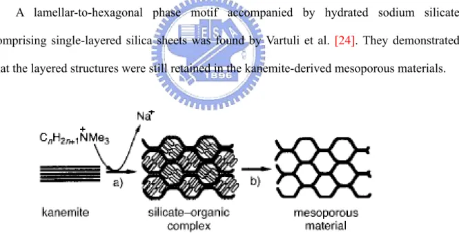
A lamellar-to-hexagonal phase motif accompanied by hydrated sodium silicate comprising single-layered silica sheets was found by Vartuli et al. [24]. They demonstrated that the layered structures were still retained in the kanemite-derived mesoporous materials.
Figure 2.5 Folding of silicate sheets around intercalated surfactant molecules. (a) Ion exchange, (b) calcination.
Under synthesis conditions that prevented the condensation of silicate species—such as low temperatures and high pH—a truly cooperative self-assembly of silicates and surfactants was found. Firouzi et al. showed that a micelle solution of
cetyltrimethylammonium bromide (CTAB) transformed to a hexagonal phase in the presence of silicate anions [25]. The silicate anions ion-exchanged with the surfactant halide counteranions to form a silicatropic liquid crystal (SLC) phase that involved silicate-encrusted cylindrical micelles. The SLC phase exhibited behavior very similar to those of typical lyotropic systems,
Figure 2.6 Formation of a silicatropic liquid crystal phase.
except that the surfactant concentrations were much lower and the silicate counteranions were reactive [26]. Additionally, Firouzi et al. also demonstrated the charge-balance requirement (electrostatic interaction) [25, 26]. There was a preferential bonding of the ammonium head group to multi-charged D4R [(Si8O20)8–] silicate anions, under high pH conditions; the interaction was so strong that an alkyltrimethylammouonium surfactant solution could force a silicate solution that did not contain D4R oligomers to re-equilibrate and form a D4R species. Furthermore, Fyfe and Fu were able to prepare mesostructured silicates with D4R silicates
[27]; they tried to combine D4R precursors with cetyltrimethylammonium chloride (CTAC) surfactant-produced mesostructured materials. Control of the condensation of the silicates within the mesostructure by acidic vapor treatment led to the observation of cubic, lamellar, and hexagonal phases as intermediate transformation phases. The M41S family comprises made up of three well-defined mesostructures: MCM-41, MCM-48, and MCM-50 [28]. Illustrations of the M41S family are provided in Figure 2.7. MCM-41 has a hexagonally packed array of noninterconnecting cylindrical pores,
Figure 2.7 Illustrations of M41S materials: (a) MCM-41, (b) MCM-48, and (c) MCM-50.
while the structure of MCM-48 can be thought of as two intertwined networks of spherical cages that are separated by a continuous silicate framework. MCM-50, meanwhile, contains a lamellar structure in the uncalcined form.
Through the acidic route, other species considered to be in the SBA series have been synthesized [29]. These materials have thicker pore walls and a framework charge that is different from those in M41S materials, due to their different precipitation conditions and charge-balance requirements. Zhao et al. have reported the synthesis of highly ordered hexagonal mesoporous silica structures named SBA-15, by using an amphiphilic block copolymer as an organic-templating agent [30]. Poly(alkylene oxide) triblock copolymers triblock copolymers ((EOx-POy-EOx))—where EO is ethylene oxide and PO is propylene
oxide—were good candidates, owing to their mesostructural ordering properties, commercial availability, biodegradability, and cost-effectiveness. The hydrothermal stability and mechanism properties of SBA-15 were superior to those of MCM-41, because the walls of SBA-15 are thicker than those of MCM-41 with cationic surfactants. The EO species had greater hydrophilicity, causing it to interact more strongly than the hydrophobic PO species (Figure 2.8). Several morphologies of mesoporous materials—such as films, spheres, hollow spheres, and fibers—have been synthesized [31–34].
Figure 2.8 A schematic diagram of SBA-15 synthesized with triblock copolymer.
Zhao et al. and Lin et al. have each synthesized hollow mesoporous silicate spheres with hierarchically ordered structures by using bitanol as a co-surfactant [35–39]. Moreover, Zhao et al. have also demonstrated a variety of SBA-15 morphologies by using a co-surfactant, co-solvent, or electrolytes [40]. Herein, the morphology of SBA-15 strongly depended on the surface curvature energy at the interface of inorganic silica and organic copolymer species.
The large pores of mesoporous materials are formed directly by copolymers called mesostructured cellular foams (MCFs). Prior to their development, large-pore molecular sieves were much in great demand, for the separations of large molecules; the development of
SBA-15 and MCF has extended the range of mesoporous materials with pore sizes larger than 10 nm [41]. On the other hand, SBA-15 and MCF materials were synthesized with triblock copolymer (EO-PO-EO) templates and are related by phase transition from a hexagonally ordered cylindrical mesoporous structure to the mesocellular foam structure.
To date, there has been increased interest in the fabrication of nanometer-sized fine structures, because of their potential utilization in electronics and optical and micromechanical devices. There have been numerous reports of the preparation of inorganic mesoporous films, due to their potential use in separation membranes, chemical sensors, optical devices, and electronic devices such as low-k dielectric films [42–44]. Most of all, the mesoporous silica of MCM-41 and SBA-15 have conventionally been fabricated by surfactant-silicate composites from a liquid phase, under acidic or basic conditions [45–47]. A simple way to synthesize mesoporous silica films has been developed using the spin-coating and dip-coating methods [48, 49]. Recently, Kim and Ryoo have synthesized MCM-48 crystals (Ia3d) with a cubic structure [50], and Che et al. have reported the synthesis of SBA-1 (Pm3n) with a large number of facets by adjusting temperature, synthesis time, acidity, and surfactant concentrations [51]. It should be noted that ionic surfactants have been used in all reports; this is because the specific interaction between copolymer and silica is much weaker than that of ionic surfactants and inorganic species in solution.
In recent years, much work has been done in which there was use of ordered mesoporous carbon, CMK-3, and mesoporous metal oxide that were synthesized through a template method from SBA-15 mesoporous silica; in much of this work, these films were used to derive electric double-layer capacitors (EDLCs) and sensing materials [52–56].
Chapter 3 Fundamentals of Semiconductor Metal Oxide
Gas Sensors
According to Göpel and Schierbaum [57], gas sensors are devices that convert a chemical state into an electrical signal. Although many authors have provided more general or specific definitions for this kind of sensor [58], this is probably the simplest one that best fits the purpose of this work. The term “chemical state” must be understood as alluding to different concentrations or partial pressures of molecules or ions in a gas, liquid, or solid phase; if these conditions are not specified, it is often assumed that these chemical sensors are just a primary link in the proverbial measuring chain—in other words, an interface of the chemical world and electronics.
Stetter and Penrose [59] indicate that good gas sensors should provide (1) a sensitive layer, (2) information regarding changes in the chemistry of the sensitive layer, and (3) a sensitive layer on a platform, allowing transduction of the change to electric signals; furthermore, they should (4) be small in size, (5) operate in real time, and (6) be cost-effective. As stated above, every chemical sensor that has ever been made belongs to one of two domains: the physical transducer or the chemical interface layer. At the chemical interface, the analyte interacts chemically with a surface, producing a change in physical and/or chemical properties. These changes are measured by the transducer domain, which monitors this change and generates a related electrical signal.
The characteristics of semiconductor metal oxide (SMO) gas sensors are based on changes in their electrical properties in the presence of a gas. Depending on the material, this change can be due to bulk effects, surface conductance effects, or a combination of the two [60]. Consequently, oxygen has free valences that result in a basic electrical conductivity when in vacuum. The gas-dependent conduction behavior of metal oxide semiconductors
relies upon the presence of oxygen in an ambient gas (e.g., the use of air). If the oxygen concentration in the ambient gas is different from the oxygen equilibrium concentration in the bulk metal oxide, oxygen diffusion takes place and the conductivity of the metal oxide changes. This is termed the “bulk effect.” At room temperature in air, oxygen is adsorbed at any surface (including the metal oxide surface); therefore, oxygen molecules react with electrons from the metal oxide surface, and so decrease the concentration of free electrons. This leads, in the case of n-type materials, to a reduction in their conductivity. The amount of adsorbed O2– depends strongly on the oxygen partial pressure. If there is a reducing or oxidizing gas present in the ambient gas that is able to react with the adsorbed oxygen, the surface concentration of the adsorbed oxygen will be altered. Normally, energy must be applied externally, to overcome internal activation energies; the common operation temperatures of SMO gas sensors are therefore in the range of 50–900°C. The reaction will take place only at the surface of the heated sensor part. To understand this surface reaction, it is necessary to consider some surface chemistry concepts.
The foundation of SMO materials is controlled through the processes discussed below.
3.1 Physisorption and Chemisorption
Gas molecules on the surface cannot fully satisfy their valence or coordination requirements. The adsorption of external species that happen to be in the vicinity of the surface reduces the surface energy of the solids. Physisorption and chemisorption would, then, occur at the same time. The gas molecules are seized by van der Waals forces (physisorption), and gas molecules adsorbed on the surfaces would result in through an exchange of electrons, resulting in chemical bonds (chemisorption).
Figure 3.2 shows a diagram of oxygen desorption from a semiconducting metal oxide sensor. As one can see, the physisorbed and chemisorbed oxygen are adsorbed point defects are formed at the surface, and bulk defects are involved.
Figure 3.1 A thermal desorption spectra (TDS) of molecular oxygen on ZnO. Curve C is the first heat treatment. [61].
3.2 Charge Transfer Model (CTM)
The Charge Transfer Model (CTM) describes the interaction at the gas/metal oxide interface. It describes the chemisorption of gas molecules in terms of “ionsorption,” where molecules are free to accept or donate electrons from the bulk material. This is equivalent to the generation of a surface state with an underlying space-charge region. Whether these surface states can act as surface acceptors or donors depends on the nature of both the adsorbed gas (i.e., whether reducing or oxidizing), as well as the type of semiconductor (i.e., whether n-type or p-type). Thus, the gas adsorption leads to a band deflection near the surface [62]. To understand the CTM, it is necessary to know the band model, the Fermi distribution, and the influence of doping. A common classification of layers considers whether the injected type of the charge carrier is of the same type as the major charge carrier (termed the “accumulation layer”) or vice versa (termed the “depletion layer”) [63]. For example: • Donors on the surface of an n-type material—which inject electrons into the conduction band—or acceptors on the surface of a p-type material—which inject holes into the valence
band—form an accumulation layer.
• Acceptors on the surface of an n-type material—which extract electrons from the valence band or donors on the surface of a p-type material—which inject electrons into the conduction band—can form a depletion layer.
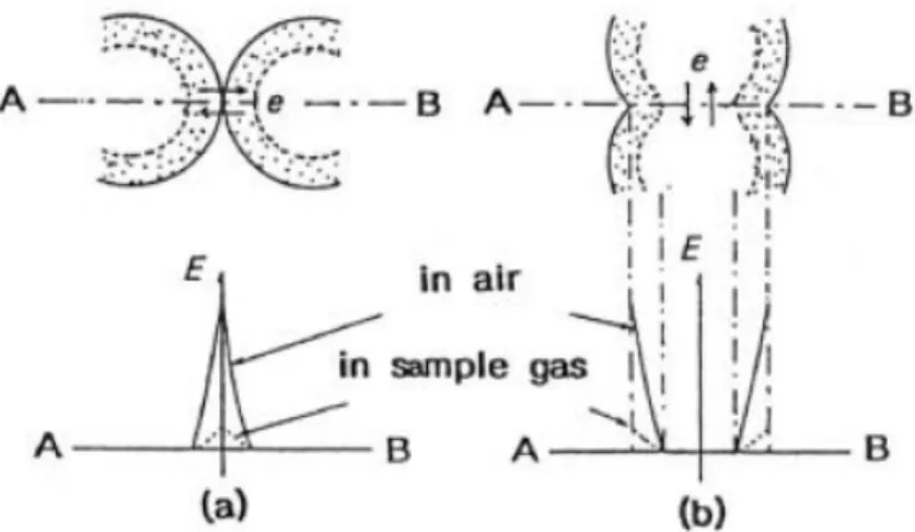
Figure 3.2 shows the influence of an adsorbed electron acceptor (e.g., O2) on an n-type and a p-type semiconductor. Owing to such a charge transfer, a positive space-charge region in the surface region is generated [62].
Figure 3.2 Space charge at the surface of an n-type semiconductor (left) and of a p-type s e m i c o n d u c t o r ( r i g h t ) , d u e t o t h e a d s o r p t i o n o f a n e l e c t r o n a c c e p t o r . (a) Distribution of the charge carrier, (b) band deflection at the semiconductor surface (c) charge carrier concentration in the conductor valence band. EC: edge of the conduction band, EV: edge of the valence band, EF: Fermi level, ED: donor level, EA: acceptor level, EI: intrinsic level, nb: concentration of electrons in the bulk, pb: concentration of holes in the bulk. [62].
3.3 Depletion Layers Effect
Each SMO gas sensor presents a depletion layer of width L in air, where L depends on the Debye length and the strength of the oxygen chemisorption. The Debye length can be expressed as:
LD = (kTε/ q2n)1/2,
where k, T, q, e, and n are the Boltzmann constant, Kelvin temperature, electron charge, dielectric constant, and charge-carrier concentration, respectively. The thickness of the space charge layer is related to Debye length (LD) is usually determined by:
L = LD * (2eVs / kT)1/2,
where eVs is the surface potential and kT is thermal energy. It follows that the introduction of impurity cations inside the lattice would result in changes in LD and L, and therefore promote or attenuate gas sensitivity, even when grain size remains the same.
Therefore, by reducing the particle size, high gas sensitivity and short response times can be achieved. Dieguez et al. showed that in the two smallest particles was found the highest density of defects, all of which could negatively influence the transport properties or act as a region for accumulating metal doping in the crystalline. Therefore, a compromise between particle size and depletion layer is ideal. To date, SMO crystals deposited by thin-film techniques have been polycrystalline; this enables the diffusion of gases along the grain boundaries, allowing the gases to influence each single grain. In this case, the ratio of grain size to effective Debye length has a significant effect on the gas-sensing behavior. To explain this behavior, an n-type semiconductor with adsorbed electron acceptors is considered (Figure 3.3); if the Debye length is smaller than half the grain size (Figure 3.3, left), then the conduction is dominated through the charge carrier depletion at the grain edges. This results in a band bending at the interface between each single grain. In the case of a larger Debye length (Figure 3.3, right), the charge depletion occurs in the whole grain and results in a movement of the complete conduction band relative to the Fermi level.
Figure 3.3 Charge carrier concentration n and conduction band EC for the contact position of g r a i n b o u n d a r i e s , f o r a g r a i n w i t h a D e b y e - l e n g t h ( LD) l e s s t h a n a half-grain size on the left side and a grain with a Debye-length more than a half-grain size on the right side.
3.4 Neck-controlled and Grain Boundary Effect
SMO gas sensors with small grain size have high gas sensitivity. However, grains are connected by neck and grain boundaries. The model combines the neck mechanism and grain boundary mechanism, because there is a charge transfer between the neck and grain boundaries. Conducting electrons should move across a potential barrier when the grain boundaries make contact. Ihokura et al. has indicated that the barrier is high, caused oxygen’s rate of adsorption is lower than that of target gases [64].
Figure 3.4 Surface space charge layer and electron transport between grain and target gases. (a) Grain boundaries, (b) necks. E: Potential energy of electrons.
When D>>2L, it is apparent that the gas sensitivity is essentially independent of grain size. When electrons transferred to a channel of nearby necks (Figure 3.4), the aperture of the channel is modulated by with the surface spacer layer; this is consistent with the findings of Mitsudo [65]. It is narrow in air, because of oxygen adsorption that occurs while a target gas arrives to consume adsorbed oxygen, leading to gas-dependant electric resistance. On the other hand, it is assumed that the space charge layer is formed to the depth of L and the electron concentration is constant, when the electron concentration in the core region is as shown in Figure 3.5. When the mobility of electrons is constant, the gas sensitivity can be expressed by:
S = Ra / Rg = (x–1)2 + nL(g) / n0 [x2 – (x–1)2] / (x–1)2 + nL(a) / n0 [x2 – (x–1)2] where x= X / 2L, and nL(g), and nL(a) are electron concentration in air and in target gas, respectively.
Figure 3.5 Assumed electron concentration profiles at the cross-section of a neck.
A simplified model consisting of a large number of necks and a small number of grain boundary contacts is demonstrated as a 1D chain of particles. The following three cases are differentiated, according to the value of D and 2L (Figure 3.6):
(a) D >> 2L (Grain boundary control). The electron channel is too wide, and the resistance at the grain boundary contacts determines the whole resistance, giving rise to a gas sensitivity that is independent of D.
(b) D = 2L (Neck control). Each channel is narrow, and since the number of necks is greater than the number of grain boundary contacts, the resistance of the entire element would rise to the neck size-dependent gas-sensitivity level.
(c) D < 2L (Grain control). Each particle is included as a whole in the space-charge region. The electron transport at any place inside the particle becomes susceptible to the surface effect, and the whole of the electrical resistance and gas sensitivity will be controlled by grains at a sufficiently small D value. The outer part of each grain is more susceptible to gases than the inner part; this likely explains the increase in gas sensitivity as D decreases, though quantitative measurements have yet to be taken.
If D is small, the depletion region will drop down the neck conduction channel. Electrons are significantly scattered by the grain boundaries, and the mobility is therefore reduced [66].
3.5 Schottky Contact
It has been proven that a change can occur in the Schottky barrier height, on account of the electron concentration adsorbed on the surface [67]. When gas molecules are adsorbed on the semiconductor surface, the Fermi level of the semiconductor adjusts to the dominating presence of the metal; the free carrier density is much higher than that of the semiconductors, and the Fermi level is lowered by an amount equal to the difference between the two work functions. An adjustment of the Fermi level occurs when there exists a thin dielectric layer, such as WO3, between the metal and the semiconductor. This scenario is illustrated in Figure 3.7, which describes the energy band diagram of the Schottky barrier structure in the absence of the surface states in the semiconductor [68].
Figure 3.7 (a) Energy-band diagram of metal-oxide-n-type semiconductor junction: (I) Before contact, (II) after contact and thermodynamic equilibrium is attained, in the presence of a gap (or an insulating dielectric) of thickness d, (III) when d is comparable to interatomic distance, and (IV) in the limit d=0 (metal-semiconductor junction).
If the barrier is high enough, the Schottky diode is rectifying (i.e., the current-voltage (I-V) characteristics are not highly linear), behaving like an ordinary p-n junction in series with a thin tunneling layer. Upon exposure to certain gases, the Schottky barrier is affected. The dependence of metal work function (qøm) indicates that a device can become gas-sensitive when Schottky diodes are exposed to gases that alter the metal work function. The bending of the semiconductor bands at the interface occurs down to a depth W, which is called the depletion width or the surface charge layer. Sricastava et al. demonstrated that the electrical behavior of n-type SMO-sensing material with active grain boundaries are controlled by the formation of double Schottky potential barriers at the interface between adjacent grains. The formation is the result of charge-trapping at the interface. Trap states present at the interfaces can capture majority carriers; therefore, the bending of the band
occurs and forms a barrier at the interface. While this material is exposed to under the air conditions, oxygen molecules are adsorbed at the surface. The adsorbed oxygen accepts electrons from the trap states present at the interface of adjacent grains, to form O2–, O–, and O2– ions—thus decreasing the concentration of the number of charge carriers nearby the surface and causing a depletion of the raised layer. When exposed to a reduced gas in air, the co-adsorption and mutual interaction between the reactants (i.e., reducing gas and oxygen gas) result in an oxidation of reducing gas at the surface [69]. The oxidation phenomenon helps in the removal of oxygen ions from the surface, resulting in a decrease of barrier and an increase in conductance.
3.6 Oxygen Vacancy
Several models explain the resistance change of SMO-sensing materials. In air conditions, the oxygen that would otherwise absorbs at the surface would dissociate to O–. The electron extraction tends to increase resistance. In the presence of a combustible gas (i.e., hydrogen), that gas would react with the adsorbed O– to form water and the electrons would be re-injected into the semiconductor, leading to a tendency to decrease the resistance.
O2 + 2e– → 2O– H2 + O– → H2O + e–
A competition results between oxygen-removing electrons and the reactive gas that restores these electrons. The steady-state value of the resistance depends on the concentration of the combustible gas. Another model shows that, if chemically active, the reactive gas would exist or coexist and extract lattice oxygen from the metal oxide, leaving vacancies that act as donors. The oxygen from the air tends to re-oxidize the metal oxide, removing donor vacancies; in this way, there is a competition between oxygen-removing donor vacancies and gas-producing donor vacancies. The density of the donor vacancies depends only on the concentration of gas, because the oxygen pressure is constant.
R + O2–
↔ RO + V+ + e–,
Chapter 4 Experimental Methods
4.1 Synthesis of Mesoporous Mmaterials4.1.1 Synthesis of Mesoporous Silica Template
Samples of the hexagonal structure mesoporous silica SBA-15 were prepared using a simple hydrothermal process, according to methods found in the literature [70, 71]. In the batch synthesis, 4 g of poly(alkylene oxide) triblock copolymer P123 (EO20PO70EO20, EO = ethylene, PO = propylene, BASF) as the structure-directing agent was dissolved into 30 g of deionized water and 120 g of 2 M HCl solution under stirring at 40°C. This was followed by the addition of 8.6 g of TEOS into the solution; it served as the silica source. The mixture was kept under static conditions in an oven for 20 h at 40°C. Subsequently, the mixture was placed in an oven at 100°C for 24 h for hydrothermal treatment. The molar ratio of composition was 0.017 P123/0.02 TEOS/0.12 HCl/3.92 H2O. Following hydrothermal treatment, the solid product was filtered, washed with deionized water, dried at 120°C overnight, and calcined at 560°C. To investigate the interconnectivity of silica templates, the mixtures were treated at different hydrothermal temperatures; the resultant SBA-15 samples are denoted as SBA-40d, SBA-60d, and SBA-100d.
4.1.2 Synthesis of mesoporous carbon
The carbon replicas were derived by the presence of silica templates, sucrose, and H2SO4 [72]. Briefly, 1 g SBA-15 was added to a solution obtained by dissolving 1.25 g sucrose and 0.14 g H2SO4 in 5 g of H2O. The mixture was heated in an oven for 6 h at 100°C. Subsequently, the oven temperature was raised to 433 K for another 6 h. The sample turned dark brown or black during heat treatment in the oven. The silica sample was treated again at 100°C and 160°C, using the same drying oven, following the addition of 0.8 g sucrose, 0.09 g H2SO4, and 5 g H2O. Carbonization was completed via pyrolysis with heating, to typically
900°C under an argon atmosphere. The carbon-silica composite obtained after pyrolysis was washed with 5 wt% hydrofluoric acid at room temperature, to remove the silica template. The template-free carbon product thus obtained was filtered, washed with ethanol, and dried at 393 K. All samples were denoted as Suc-40d, Suc-60d ,and Suc-100d.
4.1.3 Synthesis of mesostructured metal oxide materials
The mesoporous metal oxide samples were synthesized using mesoporous silica and mesoporous carbon templates. To synthesize mesoporous cobalt oxide, mesoporous silica was used as the template. Mesostructured cobalt oxide materials were prepared using SBA-15, along with different interconnectivity networks as templates. Generally, a mixture of Co(NO3)2·6H2O (0.8 M) and SBA-15 (0.2 g) was dissolved in ethanol and stirred for 1 h. The resultant materials were then calcined at a temperature of 450°C for 6 h. Finally, the silica template was removed using 5% hydrofluoric (HF) solution the black-colored Co3O4 materials were recovered by centrifugation and dried at a temperature of 50°C overnight. The samples obtained were denoted as Co-hex-40d, Co-hex-60d, and Co-hex-100d.
Previously, the mesostructured cobalt oxide was synthesized by using mesoporous silica as a template. However, mesostructured ZnO cannot synthesize with mesoporous silica, because the removal of the silica templates utilizes HF or concentrated sodium hydroxide (NaOH) solutions. Mesostructured ZnO is unsuitable for this purpose, as it is soluble when the pH is very low or very high. Therefore, mesoporous carbon is used instead of mesoporous silica as the solid template for synthesizing mesoporous ZnO. The mesoporous carbon is first prepared through a structure replication procedure, and then a mesoporous metal oxide is infused into the replica. Herein, mesostructured ZnO was prepared by immersing 0.5 g CMK-3 carbon in 20 mL of a solution comprising Zn(NO3)2 in THF (1.5 mol L−1) and stirring at room temperature for 6 h. After filtration, the impregnated carbon was dried at ambient temperature, heated in an air atmosphere to 300°C and at a constant rate of 2.5 K min−1, and
kept at that temperature for 2 h to convert zinc nitrate to zinc oxide. This procedure was repeated twice. The resultant product was a powder lacking any specific particle morphology.
4.2 Fabrication of mesostructure-sensing device
4.2.1 Fabrication of thick-film sensor device
Thick-film gas sensors were obtained via the print-screen of a paste based on alumina substrates. The alumina substrates (5 × 25 × 0.5 mm) were cleaned with acetone, alcohol, and deionized water in an ultrasonic machine. The platinum electrodes were deposited by an E-gun on the substrate. The electrodes were interdigitated, with 0.3-mm widths and 0.2-mm lengths. The mesostructured metal oxide samples were mixed with an appropriate amount of organic solvent until a homogeneous mixture was obtained. Finally, the mixture was printed on the alumina substrates, using a print-screen machine.
Figure 4.1 Schematic of the alumina substrates with the interdigitated electrodes.
4.2.2 Fabrication of thin-film sensors
To reduce power consumption, a micro-sensor device was fabricated on the silicon-based membrane, which was embedded with platinum interdigitating electrodes and a micro-heater (see Figure 4.2).
Figure 4.2 Fabrication schematic diagram of the micro-sensor device.
The details are as follows:
(a–b) A 2-µm-thick SiO2 layer was thermally grown on a p-type silicon wafer bearing a thickness of 500 µm.
vapor deposition (LPCVD).
(d–e) A thin, 240-nm film of Cr was deposited onto the Si3N4 and photoresist layers by DC-sputtering on the front side of the wafer. The Cr-resistant heater and sensor were readily formed using the lift-off technique.
(f) A 2-µm-thick SiO2 layer was deposited over the heater, using PECVD. (g) A 200-nm Si3N4 deposition was applied over the SiO2 layer, using PECVD.
(h–i) A square window pattern was opened through the SiO2 and Si3N4 layers on the back side of the wafer, using photolithography; it was then etched using a reactive ion etch (RIE). Resistance was then etched by RIE, with O2.
(j–k) A 240-nm-thick pt film was deposited on the front SiO2 layer by DC-sputtering, which was then patterned to define the bonding pads. Again, the pair of electrodes was created by using the lift-off technique.
(l) To achieve excellent thermal isolation and reduce thermal mass, the membrane was fabricated via KOH anisotropic etching on the back side of the wafer; a 2-µm-thick layer of thermal oxide was applied as an etch stop.
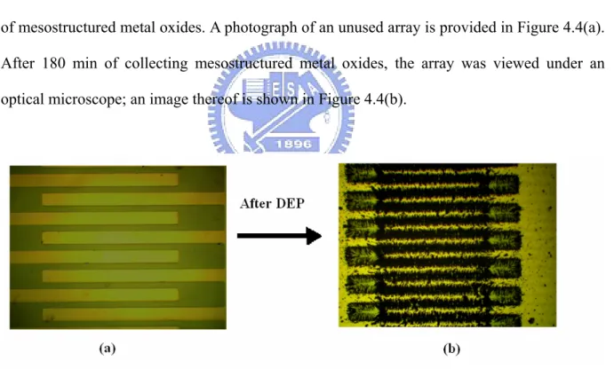
All sensing materials were immobilized on the micro-sensor device, using the DEP process. All experiments were carried out at room temperature. The experiment set-up consisted of a function generator, an oscilloscope, and a microscope. The function generator, which included a sinusoidal wave output, was used to generate the drive signal. Different drive signals—in the range of 1–10 V, peak-to-peak, with frequencies in the range of 1–3 MHz—were used during testing. First we chose the original samples, and the gaps between them were an average of 20 µm each. A 10-V voltage with a 1-MHz frequency was applied to the interdigitated-castellated design. The devices were fixed on a chip holder, which was connected to the AC signal source (GW Instek GFG-3015 function generator) and the electrodes. The chip holder was then mounted on a microscope for the real-time observation of mesostructured metal oxides. A photograph of an unused array is provided in Figure 4.4(a). After 180 min of collecting mesostructured metal oxides, the array was viewed under an optical microscope; an image thereof is shown in Figure 4.4(b).
Figure 4.4 OM images: (a) Before the DEP immobilized and (b) after the DEP immobilized the mesostructured metal oxide samples.
4.3 Characterization
4.3.1 X-ray diffraction (XRD) patterns
Bade D1 involves a powerful X-ray diffractometer that is employed to identify the phases and determine the structural properties of mesostructured sensing materials. The highly ordered symmetries of the mesostructured gas-sensing materials were identified using low-angle XRD patterns, where the diffraction patterns ranged from 0.5° to 3°; otherwise, the crystallites of the mesostructured sensing materials were analyzed using wide-angle diffraction patterns, where the patterns ranged from 20° to 70°.
4.3.2 Field-emission scanning electron microscopy (FE-SEM)
FE-SEM was used to observe the morphologies of the specimens. SEM uses second electron (SE) or backscattered electron (BSE) detectors that pass the signal to form images. The topology of the mesostructured templates and metal oxides were characterized by FE-SEM (JOEL JSM 6700F, 15 kV).
4.3.3 Transmission electron microscopy (TEM)
The morphologies of the mesostructured sensing materials were examined by TEM (JOEL 2010, 200 kV), and the crystalline of the mesostructured-sensing materials were determined by using selected areas electron diffraction (SAED) patterns.
4.3.4 Differential thermal and thermogravimetry analysis (DTA/TGA) measurement
Decomposition of the mesostructured materials was determined using a TA Q500 DTA/TGA analyzer. The composites were examined from 25 to 700℃ ℃ (i.e., a heating rate of 10 /min)℃ .
XPS measurements were carried out using a PHI 1600 (Perkin Elmer) with a Mg Kα X-ray at 250 W. The analyzer angle of the X-ray source was 54.7°. Based on the high-resolution spherical capacitor analyzer (SCA), the energy resolution was 1.5 eV for the survey scan spectra.
4.4 Gas-sensing measurement
A diagram of the testing chamber is shown in Figure 4.5.
Figure 4.5 The diagram of the mesostructured materials testing chamber.
The purpose of this study was to determine the optimal conditions of mesostructured gas sensors for gas-detecting, including operating temperature, gas concentrations, response time, and recovery times. To that end, we defined the response and recovery times as follows, respectively: ζres = t90% – t10%, where t100% is the time at which the conductance has reached the stable state, and ζrec = t10% – t90% [75]. In general, the sensitivity of the gas-sensing materials was defined as the percentage change of the sensor resistance present in the target gas and dried air. The definition of the sensing materials is as follows (S%):
S% = (Rgas – Rair / Rair) × 100 (For p-type materials) Otherwise, it was defined as:
S% = (Rair – Rgas / Rair) × 100 (For n-type materials), where Rair is the resistance in dried air and Rgas is the resistance in the target gas.
Sensors were placed in a furnace test chamber. A continuous flow of gas (100 ml/min) passed through the chamber, making the pressure in the chamber nearly atmospheric. The desired gas concentration was obtained by mixing the appropriate flows of gases by means of mass flow controllers the electrical resistance response during testing was monitored by using a precision analyzer (Keithley 2400).
Chapter 5 Results and Discussion
5.1 Mesoporous silica template
5.1.1 Synthesis of SBA-15 at different temperatures
Recently, hexagonal-templated silica with a large surface area (700–900 m2 g–1), large pore size (5–9 nm), and thick walls (3.5–5.3 nm), called SBA-15, has been detailed by Zhao et al. [76, 77]. The SBA-15 synthesizes with non-ionic surfactants, displays excellent interfacial stabilization properties and is low-cost, nontoxic, and biodegradable. Figure 5.1 shows the XRD patterns of as-synthesized SBA-15, prepared with EO20PO70EO20 as the structure-directing agent. This figure shows that there are three obvious well-solved peaks that can be indexed as (100), (110), and (200) diffraction peaks with p6mm hexagonal symmetry. For the as-synthesized SBA-15, the intensity of the (100) peak reflects a d-spacing of 9.6 nm, accompanied by a larger cell parameter whose a0 value was 11.1 nm. To show the morphology of the SBA-15 template, an SEM image of SBA-15 is provided in Figure 5.2. A rod-like structure with a 2-µm length and 400-µm diameter can be seen in the square regions. Some aggregate of SBA-15 can also be observed in the elliptical regions.
The nitrogen adsorption-desorption isotherm and corresponding pore-size distribution is shown in Figure 5.3. The isotherm reveals a well-resolved type-IV isotherm, with a sharp capillary condensation step indicative of mesopores that are narrowly distributed in size. The surface area, pore size, and total pore volume of the SBA-15 was 914.2 m2 g–1, 9.02 nm, and 1.3 cm3 g–1, respectively. The SBA-15 has a larger pore size and pore volume than MCM-41; on the other hand, the mean thickness of SBA-15 is about 5 nm, which is substantially thicker than the pore wall of MCM-41 silica (1~2 nm). Thus, SBA-15 exhibits the excellent hydrothermal properties, mechanism stability, and rapid catalysis reactions.
0.5 1.0 1.5 2.0 2.5 3.0
SBA-15
Intensi
ty
(a.u.)
2
θ(degree)
Figure 5.1 XRD patterns of as-synthesized SBA-15 template.
0.0 0.2 0.4 0.6 0.8 1.0 0 200 400 600 800 1000 SBA-100
Vol. Adsorbed (cm
3/g)
P/P
0(Relative Pressure)
0 100 200 300 400 500 9.02 nmdV/dW
Pore Size (A)
Figure 5.3 (a) Nitrogen isotherms of as-synthesized SBA-15 and (b) the corresponding pore-size distribution.
(b) (a)
In general, variations in aging temperature are not only affected by the morphology, microporosity, and connection, but also by the tuned pore size and different silica pore-wall thicknesses [78]. Figure 5.4 shows the XRD patterns of SBA-15 synthesized at 40°C, 60°C, and 100°C. The diffraction pattern of SBA-100d shows three peaks that can be indexed according to a hexagonal array of mesopores, as for MCM-41; reflections due to the diffraction planes (100), (110), and (200) are observed. However, it can be seen that only one peak can be obtained with SBA-40d and SBA-60d. For the SBA-15 synthesized at a different temperature (i.e., from 40°C to 100°C), the cell parameter of the SBA-15 was different. The cell parameter of SBA-100d was around 11.1 nm; however, shrinking was observed for the SBA-15 synthesized between 40°C and 60°C (9 nm), likely due to the incomplete condensation of silica at low temperatures. For samples prepared at temperatures above 80°C, the cell parameter of SBA-15 sample was 11 nm. Figure 5.5 reports the nitrogen adsorption-desorption isotherms and pore-size distributions, respectively, for the series of SBA-15 materials synthesized with an increasing temperature during hydrothermal treatment. The sorption isotherms for the different calcined samples all remained well-resolved type-IV isotherms, with a sharp capillary condensation step indicative of mesopores that were narrowly distributed in size, irrespective of temperature. The shift of the capillary condensation step to a higher relative pressure and an increased temperature with mesopore size is also indicated by the evolving pore-size distribution curves. The surface area, pore size, and total pore volume increased sensibly, with an increase in temperature. The surface areas of all samples increased from 578.9 to 914.2 m2 g–1, the pore size from 4.5 to 9.0 nm, and the total pore volume from 0.61 to 1.3 cm3 g–1, respectively.
0.5 1.0 1.5 2.0 2.5 3.0 SBA-100d SBA-60d SBA-40d
Inte
nsity
(a.u.)
2
θ
(degree)
Figure 5.4 XRD patterns of SBA-15 synthesized at 40°C, 60°C, and 100°C.
0.0 0.2 0.4 0.6 0.8 1.0 0 200 400 600 800 1000
SBA-100d
SBA-60d
SBA-40d
V
o
l. Adsorped (c
m
3/g
)
Relative Pressure (p/p
0)
0 100 200 300 400 SBA-100d SBA-60d SBA-40d Pore Volume (cm 3 g -1 )
Pore Size (A)
Figure 5.5 (a) Nitrogen adsorption-desorption isotherms and (b) pore-size distribution of SBA-15 synthesized at 40°C, 60°C, and 100°C.
Figure 5.6 SEM images of SBA-15 synthesized at different temperatures: (a) 40°C, (b) 60°C, and (c) 100°C.