國
立
交
通
大
學
電機與控制工程系
碩
士
論
文
離散時間單迴路積分三角類比數位轉換器之功
率損耗模型建立與針對非對稱數位用戶迴路終
端機應用之電路設計
Building the power consumption model of discrete time
single-loop multi-bit sigma-delta ADC and designing the circuit for
ADSL-CO (central office) application
研 究 生:徐基恩
指導教授:陳福川 教授
離散時間單迴路積分三角類比數位轉換器之功率損耗模型
建立與針對非對稱數位用戶迴路終端機應用之電路設計
Building the power consumption model of discrete time single-loop
multi-bit sigma-delta ADC and designing the circuit for ADSL-CO
(central office) application
研 究 生:徐基恩 Student:Chi-En Hsu
指導教授:陳福川 Advisor:Fu-Chuang Chen
國 立 交 通 大 學
電 機 與 控 制 工 程 系
碩 士 論 文
A ThesisSubmitted to Department of Electrical and Control Engineering College of Electrical Engineering and Computer Science
National Chiao Tung University in partial Fulfillment of the Requirements
for the Degree of Master
in
Electrical and Control Engineering
August 2007
Hsinchu, Taiwan, Republic of China
離散時間單迴路積分三角類比數位轉換器之功
率損耗模型建立與針對非對稱數位用戶迴路終
端機應用之電路設計
研究生:徐基恩 指導教授:陳福川 教授 國立交通大學 電機與控制工程研究所摘要
在本篇論文中,我們建立了積分三角類比數位轉換器的功率消耗模型,而我們把功率 消耗模型分成類比功率消耗模型和數位功率消耗模型兩個部份,類比功率消耗模型包括 積分器功率消耗模型、量化器功率消耗模型、數位類比轉換器功率消耗模型;數位功率 消耗模型包括時脈產生器功率消耗模型和開關功率消耗模型。 我們針對非對稱數位用戶迴路終端機應用來做電路設計。我們選擇的電路架構為離散 時間單迴路單一位元積分三角類比數位轉換器來實現非對稱數位用戶迴路終端機。Student:Chi-En Hsu Advisor:Dr. Fu-Chuang Chen
Institute of Electrical and Control Engineering Nation Chiao Tung University
ABSTRACT
In this work, we build the power consumption model of discrete time single-loop multi-bit sigma-delta ADC, and the power consumption model of discrete time single-loop multi-bit sigma-delta ADC can be divided into two parts. The one is the analog power consumption model, and the other is the digital power consumption model. The analog power consumption model includes the integrator power consumption model, the Quantizer power consumption model and the DAC power consumption model. The digital power consumption model includes the clock driver power consumption model and the switch power consumption model.
We design the circuit for ADSL-CO (central office) application. And we used the discrete time single-loop single -bit sigma-delta ADC architecture to simulate.
Building the power consumption model of discrete
time single-loop multi-bit sigma-delta ADC and
designing the circuit for ADSL-CO (central office)
誌
謝
首先感謝陳福川老師在我的研究論文方面的指導,使我的論文能夠更完善,並且在 ic 設計的領域建立的一定的基礎;接下來要感謝的是邱俊誠老師在微機電製程、8051 單晶片與 ZigBee 無線感測網路方面的指導,使我能夠在各方面都有一定的基礎,以後 能有更完善的能力去應對工作上的需求。 接下來要感謝的是研究室的同窗好友孟學、哲安、一帆、嘉宏、亞書與建賢的陪伴, 使的我在研究的路上感到不孤單;也要感謝研究室的學弟們陪伴我度過研究所最後一 年,使研究所的生活能夠多采多姿;接下來要感謝的是 314 的室友們的陪伴,使的研究 以外的生活能夠完全放鬆。 最後要感謝的是我的父母親與我的家人,有他們在精神及物質方面的支持,我才有 半碼這麼無後顧之憂的完成學業,將來的我ㄧ定更加的懂事,也會盡ㄧ切努力讓你們覺 得驕傲。
List of Symbols
Symbols
VLSB Quantizer step size
OSR OverSampling Ratio
n Order of the Sigma-Delta modulator
B Number of bits in the quantizer
S
f
Sampling FrequencyB
f Signal Bandwidth
ref
V Reference Voltage of the quantizer
A Gain of OTA
in
f Frequency of the input signal
i
φ ith phase of a nonoverlap clock
in
A
Amplitude of input signal.
jit
σ standard deviation of clock jitter
S
C
Sampling capacitorI
C
Integrating capacitorL
C
Load capacitor of OTAS
V Input signal plus feedback DAC signal
1
τ Time constant of input branch
VS
σ Standard deviation of VS
2
τ Time constant of integrator output settling
i
a gain coefficient of i th integrator
η percentage of the bottom plate parasitic
T Absolute temperature
R Switch ON resistance
N quantizer levels
Lists of Tables
Table 4.1 Standard deviations of
V
S vs. different quantizer bit numbers... 55 Table 5.1 Minimum SR and GBW required w. r. t. OSR
... 76 Table 5.2 Simulation results of standard deviation of capacitor mismatch vs. unit DAC
number with Ain=1
Lists of Figures
Fig. 1.1 ADSL band allocation (DUS, FDD)……… 2
Fig. 2.1(a)Original signal spectrum (b)Sample function when fs > 2fB (c)Signal spectrum that is sampled by (b) (d)Sample function when fs < 2fB (e)Signal spectrum that is sampled by (d)……….. 5
Fig. 2.2 Quantization process………... 6
Fig. 2.3 Quantization error caused by A/D converter……….. 6
Fig. 2.4 Quantization error range………. 7
Fig. 2.5 P.D.F of quantization error………. 7
Fig. 2.6 Sampling system………. 9
Fig. 2.7 Noise distribution after sampling……… 10
Fig. 2.8 (a)General ΣΔ modulator (b)Linear model with quantization noise……….. 12
Fig. 2.9 Noise shaping………. 13
Fig. 3.1 Block diagram of ΣΔ A/D converter………... 15
Fig. 3.2 First-order ΣΔ modulator……… 16
Fig. 3.3 Single-loop second order ΣΔ modulator……… 18
Fig. 3.4 Comparison of noise shaping techniques………... 20
Fig. 3.5 Single-loop high order ΣΔ modulator………. 21
Fig. 3.6 Four-order interpolative architecture………. 21
Fig. 3.7 2-1 architecture MASH ΣΔ modulator………... 23
Fig. 3.8 SNR vs. OSR with different quantizer bit number……… 25
Fig. 3.9 Multi-bit architecture………. 26
Fig. 3.11 Operation principle of the DWA algorithm……… 28
Fig. 3.12 Output spectrum with three kinds of DAC………. 29
Fig. 3.13 Comparison of ΣΔ modulator architectures………. 30
Fig. 3.14 Performance characteristic of a ΣΔ converter……….. 33
Fig. 4.1 A single-stage telescopic OTA……….. 38
Fig. 4.2 The folded cascode OTA……….. 39
Fig. 4.3 The two-stage Miller-compensated OTA………. 42
Fig. 4.4 An overview of the obtained data points……….. 45
Fig. 4.5 (a) Implementation of the integrator and the feedback DAC (b) To charge the unit capacitance (c) To discharge the unit capacitance……… 47
Fig. 4.6 (a) an ideal inverter for logic level with a load capacitance (b) an ideal CMOS inverter for transistor level with a load capacitance (c) an ideal CMOS inverter for transistor level with a load capacitance………. 51
Fig. 4.7 The clock generator with non-overlapping clocks……… 52
Fig. 4.8 The CMOS switch………. 53
Fig. 5.1 Fully differential switched-capacitor integrator and timing diagram… 60 Fig. 5.2 Folded cascode op-amp………. 63
Fig. 5.3 Regulated cascaded gain stage………... 65
Fig. 5.4 Gain boosting in cascode stage……….. 66
Fig. 5.5 Gain boosting folded cascode op-amp………... 66
Fig. 5.6 A wide-swing constant-transconductance bias circuit……… 67
Fig. 5.7 Simulated bias output voltages………... 72
Fig. 5.9 The gain-boosting folded-cascode OTA……… 75
Fig. 5.10 Simulated frequency response of the amplifier………... 76
Fig. 5.11 Regenerative latch comparator………. 78
Fig. 5.12 The dynamic comparator with a pre-amplifier input stage………….. 79
Fig. 5.13 Simulated output vs. input voltage of the comparator………. 80
Fig. 5.14 Input and output waveform of the comparator……… 80
Fig. 5.15 Two-phase non-overlapping clock generator……….. 81
Fig. 5.16 Relationship of the simulated clock signals……… 83
Fig. 5.17 (a) sampling mode for a switch-capacitors integrator (b) a sampling circuit, (c) a simplified sampling circuit………. 84
Fig. 5.18 Definition of speed in a sampling circuit………. 85
Fig. 5.19 Types of sampling switches………. 86
Fig. 5.20 Simulated on-resistance of switches……… 88
Fig. 5.21 Schematic of modulator circuit……… 89
Contents
中文摘要……… I English Abstract………. II List of Symbols……….. III Acknowledgment……….. IV Lists of Tables……… V Lists of Figures……….. VI Contents………. IX Chapter 1 Introduction………. 1 1.1 Motivation……… 1 1.2 Organization………. 2
Chapter 2 Fundamental Theorems of Sigma-Delta Modulators……….. 3
2.1 Nyquist Sampling Theorm ………... 3
2.2 Quantization Noise and Peak SNR……… 5
2.3 Techniques of Sigma-Delta Modulator……….. 8
2.3.1 Oversampling Technique……… 9
2.3.2 Noise shaping………. 11
Chapter 3 Architectures of Sigma-Delta Modulator……… 15
3.1 First-Order Sigma-Delta Modulator……….. 16
3.2 Single-Loop Second-Order Sigma-Delta Modulator………. 18
3.3 Single-Loop High Order Sigma-Delta Modulator………. 20
3.4 InterpolativeSigma-Delta Modulator……… 21
3.5 MASH Architecture……… 22
3.6 Multi-bit Quantizer Sigma-Delta Modulator………. 24
3.7.1 Randomization Technique……… 27
3.7.2 Data Weighted Averaging (DWA)……… 28
3.8 Decimator……… 30
3.9 Performance Metrics for a ΣΔ Modulator……… 31
Chapter 4 Models of Multi-Bit Sigma-Delta Modulator Power………. 34
4.1 Integrator power……… 34
4.2 Quantizer power……….. 43
4.3 DAC Power………. 45
4.4 Clock driver power and switch power ………... 47
4.5 Verification for the power consumption model... 56
Chapter 5 Circuit Implementation for Second-order One-bit Sigma-Delta Modulators . ………... 58
5.1 Switched-Capacitor Integrator Design……… 58
5.2 Operational Transconductance Amplifier……… 60
5.2.1 Folded Cascode OTA………. 61
5.2.2 Gain Enhancement Technique……… 64
5.2.3 Bias circuit……….. 67
5.2.4 Common-Mode Feedback……….. 72
5.2.5 Design of the Gain boosting folded cascode op-amp……. 74
5.3 Comparator………... 77
5.4 Clock generator……… 81
5.5 Switch……….. 84
5.6 Simulation of System Circuit……….. 89
Chapter 6 Conclusions and Future works……… 91
Chapter 1
Introduction
1.1 Motivation
Sigma-Delta A/D converters have become popular for high-resolution medium-to-low-speed applications such as digital audio [Bos 88][Nor 89], voice codec, and DSP chip. Recently, ΣΔ ADCs have been applied to higher bandwidth signals, and low power designs are frequently emphasized. For example, in ×DSL [Gag 03][Rio 04] applications, signals up to several MHz must be handled.
The power consumption of the Sigma-Delta A/D converters is very important in all kinds of application. So it is very important that how to design can get the better power consumption. We propose an power consumption model to estimate the power consumption in the discrete time single-loop multi-bit ΣΔ ADCs design.
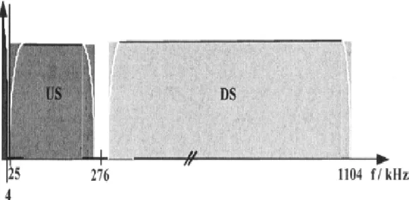
As illustrated in Fig. 1.1, As illustrated in Fig. 1, in an ADSL modem the downstream data (DS) are transferred at higher frequencies in a wider band as compared to the upstream data (US). Flexible band allocations are standardized, such as frequency division (FDD), frequency overlapping, single upstream (SUS), and double upstream (DUS).1 The developed converter targets a central-office (CO) line-card application. For such transceivers, the analog-to-digital converter (ADC) typically requires 14-bit resolution over an analog signal bandwidth of 276 kHz.
Fig. 1.1 ADSL band allocation (DUS, FDD).
1.2 Organization
This work is organized as follows. In Chapter 2 and Chapter 3, systematic studies of fundamental theory and various architectures of ΣΔ modulator are presented first. In Chapter 4, the power consumption model is derived and verified.In Chapter 5, design the circuit for ADSL-CO application. Conclusions and future works are presented in Chapter 6.
Chapter 2
Fundamental Theorems of Sigma-Delta
Modulators
Before we establish the error models of ΣΔ modulators, several important theorems and concepts must be known, such as Nyquist sampling theorem, quantization error and the two most critical techniques in a ΣΔ modulator: oversampling and noise shaping. All topologies of ΣΔ modulators are based on these two techniques. There also have some parameters we must to understand, such as OSR, SNR, and SNDR …etc. This chapter starts from fundamental theorems, and introduces several topologies of ΣΔ modulators.
We will illustrate quantization error and analyze quantization noise in an ideal A/D converter and then derives the peak signal-to-noise ratio. The resolution of an A/D converter is determined by signal-to-noise ratio, which is a very important specification in an A/D converter.
2.1 Nyquist Sampling Theorem
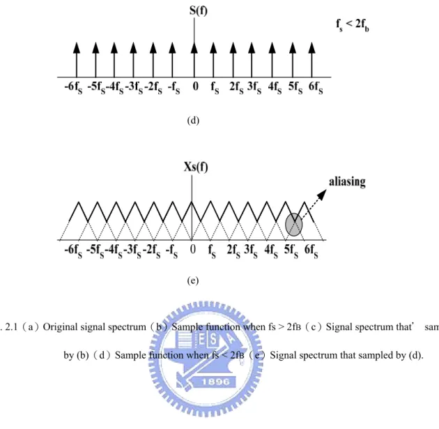
In an analog-to-digital converter, the analog signal from external environment must be converted to discrete-time signal by sampling. However, the sampling rate (fs) and signal bandwidth (fB) must follow the Nyquist sampling theorem in (2.1):
The sampling rate must be higher or equal to twice of signal bandwidth in order to prevent from aliasing. We will illustrate the phenomenon of aliasing by Fig. 2.1. Fig. 2.1(a) and (b) are the spectrums of signal and sample function respectively; from fig. 2.1(c), when sampling rate is twice higher than signal bandwidth, the signal after sampling has no aliasing and it can be perfectly reconstructed by using low pass filters. However, in Fig. 2.1(d), when the sampling rate is lower than twice of signal bandwidth, aliasing will appear in the signal after sampling. The signal having aliasing is difficult to reconstruct to original signal [Mach 96], like Fig. 2.1(e).
(a) (b) (c)
(d)
(e)
Fig. 2.1(a)Original signal spectrum(b)Sample function when fs > 2fB(c)Signal spectrum that' sampled by (b)(d)Sample function when fs < 2fB(e)Signal spectrum that sampled by (d).
2.2 Quantization noise and Peak SNR
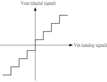
We can get a discrete-time signal by sampling a continuous-time signal, and this sampled signal can be converted to digital signal. Quantization will appear in this process, the basic concept of quantization is to classify the original signal to different levels according to its level to determine the bit number of this signal, as shown in Fig. 2.2.
Fig. 2.2 Quantization process
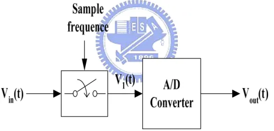
It will have quantization error even in an ideal analog-to-digital converter. As shown in Fig .2.3, we convert the digital signal B to analog signal V1 by a D/A converter, and then the
signal V1 is subtracted by input signal Vin. The result is the quantization error VQ, as in (2.2)
[Joh 97].
VQ = Vin – V1 (2.2)
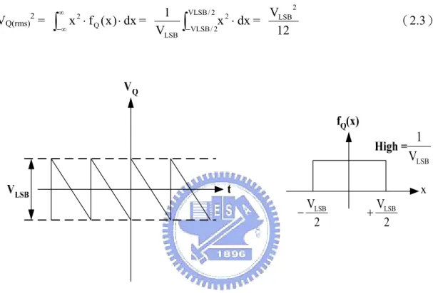
The range of quantization error is limited in ±VLSB/2 (as in Fig. 2.4), and we assume the
probability density function of quantization error is uniformly distributed between ±VLSB/2
and its mean is zero, as shown in Fig. 2.5. From this assumption, we can easily get the quantization noise power VQ(rms)2 in (2.3).
VQ(rms)2 =
∫
∞ ∞ − x ⋅fQ(x)⋅dx 2 =∫
− ⋅ 2 / VLSB 2 / VLSB 2 LSB dx x V 1 = 12 VLSB2 (2.3) 2 VLSB + 2 VLSB − LSB V 1Fig. 2.4 Quantization error range Fig. 2.5 P.D.F of quantization error
From (2.3) we can know the quantization noise power is proportional to square of VLSB, and
VLSB can be represented as in (2.4). Therefore, we can say that the quatization noise will
reduce by increasing quantization bit number.
VLSB = B
2 FS
(2.4)
FS=Full scale = Vref+-Vref- B:Quantization bit number
Vin(rms)2 is as (2.5). In (2.5), we define the amplitude of input signal is the full scale of
reference voltage, and from (2.3), (2.4) and (2.5), the peak SNR(Peak Signal-to-Noise Ratio) can be derived as in (2.6). Vin(rms)2 =
∫
− ⋅ ⋅ 2 / T 2 / T 2 dt ) t sin A ( T 1 ω = 2 A2 = 8 ) A 2 ( 2 = 8 FS2 (2.5) PSNR = 10 log( 2 ) rms ( Q 2 ) rms ( in V V )= 6.02B + 1.76 dB (2.6)(2.6) is the result obtained by Nyquist sampling rate. From (2.6), we can know that each additional bit number in quantizer increases 6dB in SNR. In Nyquist A/D converters, increasing the resolution of quantizer (decrease VLSB) while reducing the quantization noise is
a general method to reach higher SNR, but this method is sensitive to mismatches of analog device. Therefore, the general Nyquist A/D converter is not easily to implement with high resolution.
2.3 Techniques of Sigma-Delta Modulator
ΣΔ A/D converters are based on oversampling and noise shaping to reach high resolution.
Oversampling means the sampling rate is much higher than Nyquist rate, about 8~512 times in general applications. The goal of oversampling is to expand quantization noise to wider range. It can reduce the quantization noise in signal bandwidth and increase the DR (Dynamic range) of input signal. Noise shaping is a technique that moves noise to high frequency, which is done by using discrete time filter and feedback technique. After noise shaping, the noise in high frequency can be filtered out by a digital filter [Nor 97].
2.3.1 Oversampling Technique
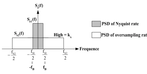
First, we made the assumption that quantization noise is a uniform distribution in sampling spectrum so its mean is zero and is a white noise [Raz 01]. The system in Fig. 2.6 just has oversampling function and does not have noise shaping effect. If a A/D converter is sampled in Nyquist rate, then the quantization noise is uniform distributed between ±fB ; if it
is sampled by oversampling technique, then quantization noise is uniform distributed between± fS2/2s, which is much larger than fB. As shown in Fig. 2.7, if the signal bandwidth is
between ±fB, then quantization noise in this bandwidth will be reduced by using oversampling
technique, which will raise PSNR significantly.
2 fS1 2 fS1 − 2 fS2 2 fS2 −
Fig. 2.7 Noise distribution after sampling
In the condition of oversampling, the PSD (Power Spectrum Density) of quantization noise is as Se2(f) in Fig. 2.7 and can be represented as:
kx2 = s 2 LSB f 12 V ⋅ = Se2 2(f) (2.7)
From (2.7) we can estimate the quantization noise in 2fB after oversampling
PQ =
∫
− ⋅ B B f f 2 x df k = OSR 2 12 FS 12 V f f 2 B 2 2 2 LSB s B ⋅ ⋅ = ⋅ (2.8)In (2.8), we define a parameter OSR (Oversampling Ratio) as
OSR = B s f 2 f (2.9)
PSNR = 10 log( Q signal P P )= 6.02B + 1.76 + 10 log(OSR) (2.10)
From (2.10), we can find that doubling OSR will increase 3dB in PSNR, which is about 0.5 bit increase in resolution. Although oversampling can reduce quantization noise, it is difficult to reach high SNR when using a low bit quantizer. For example, if we need a 16bit A/D converter, then SNR must be equal to 98dB, if the signal bandwidth is 20KHz, then the sampling rate must equal to 2 × 109 × 20KHz, it is impossible to implement. Because at such high frequency, quantization noise is no longer a white noise, it is correlated with input signal. So there is not only oversampling technique, we must add noise shaping technique also, if we want to achieve high resolution.
2.3.2 Noise Shaping
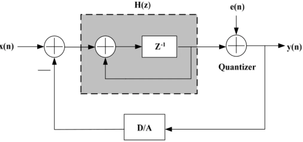
We can model a general ΣΔ modulator and its linear model as shown in Fig. 2.8.
(b)
Fig. 2.8 (a) General ΣΔ modulator (b) Linear model with quantization noise
From Fig. 2.8(a), we can derive output Y(z) as (2.11)
Y(z) = ) z ( H 1 ) z ( H + X(z) + 1 H(z) 1 + E(z) (2.11) and define Signal Transfer Function STF and Noise transfer function NTF as
STF (z)= ) z ( H 1 ) z ( H ) z ( X ) z ( Y + = (2.12) NTF (z)= ) z ( H 1 1 ) z ( E ) z ( Y + = (2.13)
where H(z) is the transfer function of a discrete time filter. There have two important meanings in (2.12), (2.13). If we want to obtain highest SNR, STF must be equal to 1, that
means the input signal can transfer to output without attenuating; and NTF (z) must be equal to
0, because the quantization noise will not affect output SNR.
In order to make NTF (z) be a high pass filter, so at DC(z = 1), NTF must be 0, and z = 1 is
H(z) = 1 Z 1 − = 1 1 Z 1 Z − − − (2.14) Substitute (2.14) into (2.12) and (2.13), we can get
STF (z) = z 1 (2.15) NTF (z) = z 1 1− (2.16)
And we substitute z with fs f 2 j
e
π
, then we can plot STF(f)2 and NTF(f)2 in frequency domain,
as Fig. 2.9. We can find NTF(f) 2 also increases with frequency, and STF(f)2 is always equal
to 1, if we choose signal bandwidth in low frequency, then we can get highest signal power and lowest noise power, from this figure we see that quantization noise is moved to higher frequency significantly, this is the noise shaping effect.
2 TF
(
f
)
N
2 TF(
f
)
S
. Fig. 2.9 Noise shapingAfter noise shaping, we can filter out the noise in high frequency by using digital filter, and we will illustrate its architecture more detail in the next chapter.
Chapter 3
Architectures of Sigma-Delta Modulator
Before we introduce various architectures of ΣΔ modulators, we must to realize the basic architecture of a general ΣΔ A/D converter. Fig. 3.1 is a complete block diagram of a
ΣΔ A/D converter [Joh 97], and we can divide it into two different parts. First part is the ΣΔ modulator. The main function of this part is doing oversampling and noise shaping to the input analog signal. Second part is the decimation filter. The main function of this part is to remove noise in high frequency and down sampling the sampling frequency to base band frequency.
. Fig. 3.1 Block diagram of ΣΔ A/D converter
First, the input signal Xin(t) pass an Anti-aliasing filter, the 3dB frequency of this filter is about few times of Nyquist frequency, so signal and noise out of Nyquist frequency is filtered roughly, and this signal goes into the ΣΔ modulator after goes through a S/H circuit. However, in the circuits implement situation, the sample and hold function is included in the circuits of ΣΔ modulator, so the signal Xc(t) will pass this modulator and produces a high speed data code Xdsm(n), because of noise shaping, the quantization noise will appear in high frequency. Finally, we must filter the noise in high frequency and reduce the sampling
frequency to Nyquist frequency by a decimator, and passes the digital signal to the output [Joh 97].
In this chapter, we will focus on the architectures of ΣΔ modulator, because that the noise model and optimal method is focus on this part, we must understand the theorem, benefits and drawbacks of each kinds of ΣΔ modulators. In addition, the implement of decimator is very typical [Ner 02][Mok 94]. In today’s technology, DSP processors are also used to replace decimators, so we will introduce this part roughly.
3.1 First-Order Sigma-Delta Modulator
We recall that H(z) in (2.14) is 1 1 Z 1 Z − −
− , substitute it into Fig. 2.8, then we can get a first-order ΣΔ modulator; Analyze transfer function H(z) from time-domain, it indicates that output signal m(t) is obtained by adding the delayed input signal n(t-1) and the delayed output signal m(t-1), so we can express a complete first-order ΣΔ modulator as Fig. 3.2.
H(z) in Fig. 3.2 is indicated the effects of delay and accumulation, this is equivalent with an integrator in circuit design, so the three circuits components of ΣΔ modulator are integrator, quantizer and DAC in the feedback path.
A first order ΣΔ modulator’s output can represent as
Y(z) = z-1X(z) + (1-z-1)E(z) (3.1)
From (3.1) we can find the signal transfer function is as a delay function, and noise transfer function is as a high pass filter, moves the noise to high frequency. In order to derive PSNR of first order ΣΔ modulator, we must get the magnitude of NTF(z) and STF(z) in the frequency
domain, so we substitute z with ej2π⋅f/fs, and get S (f)
TF and NTF(f) respectively as:
s f/f j2π 1 TF(f) z e S = − = − ⋅ = 1 (3.2) NTF(f) = 1-e−j2π⋅f/fs= j f/fs s e j 2 ) f f sin(π × × −π⋅ ⇒ ( ) 2 sin( ) s TF f f f N = ⋅ π (3.3)
So the quantization noise in base band ±fB can obtain by (2.7) and (3.3)
PQ = df f f sin 2 f 12 V df ) f ( N ) f ( S 2 f f s s 2 LSB 2 TF f f 2 e B B B B ⋅ ⎥ ⎦ ⎤ ⎢ ⎣ ⎡ ⎟⎟ ⎠ ⎞ ⎜⎜ ⎝ ⎛ ⋅ ⋅ = ⋅
∫
∫
− − π (3.4)Because that fB is much lower than fs, so sin(π f/fs) is approximate equal to (π f/fs), and PQ is
PQ = 3 2 2 LSB ) OSR 1 ( 36 V ⋅ π = 2B 3 2 2 OSR 2 36 FS ⋅ ⋅ ⋅π (3.5)
From (2.5) and (3.5), if we have the maximum signal power, then PSNR is as (3.6)
PSNR = 10 log( Q signal P P ) = 10 log( 22B 2 3 ) + 10 log[ 3 2 (OSR) 3 π ] = 6.02B + 1.76-5.17 + 30 log(OSR) (3.6)
From (3.6), we find that each octave of OSR, PSNR will increase 9dB, increase 1.5 bit in resolution. Compare (3.6) with (2.10) that only has oversampling effect; we can find that 1st order noise shaping increases the performance of ΣΔ modulator.
3.2 Single-Loop Second-Order Sigma-Delta Modulator
When the discrete time filter in Fig. 2.8 is replaced by two cascade integrator, then it is a second order ΣΔ modulator, output of the first integrator is only connecting with the input of the second integrator, it is shown in Fig. 3.3
Then the output of it can easily be derived as
Y(z) = z-2X(z) + (1-z-1)2E(z) (3.7)
where STF and NTF is as
STF(z) = z-2 (3.8)
NTF(z) = (1- z-1)2 (3.9)
Using the same method in (3.3) (3.4), we can obtain
1 ) f ( STF = (3.10) 2 s TF f f sin 2 ) f ( N ⎥ ⎦ ⎤ ⎢ ⎣ ⎡ ⎟⎟ ⎠ ⎞ ⎜⎜ ⎝ ⎛ ⋅ = π (3.11) PQ = 5 4 2 LSB OSR 60 V ⋅ ⋅π = 2B 5 4 2 OSR 60 2 FS ⋅ ⋅ ⋅π (3.12)
So finally, PSNR of the second order ΣΔ modulator is as
PSNR = 10 log( Q signal P P ) = 10 log( 22B 2 3 ) + 10 log[ 5 4 (OSR) 5 π ] = 6.02B + 1.76-12.9 + 50 log(OSR) (3.13)
In the single loop second order architecture, each octave of OSR can increase PSNR by 15 dB, it is equivalent to 2.5 bit in resolution. If we compare (3.13), (3.11) with NTF(f) =1 that
quantization noise is highest when NTF(f) =1, and that with second order noise shaping is
smallest among this figure [Joh 97].
TF
N
2
f
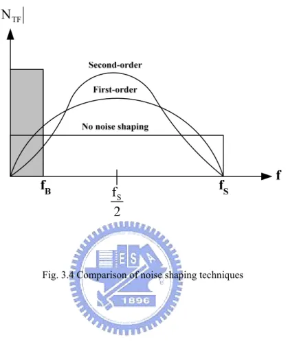
SFig. 3.4 Comparison of noise shaping techniques
3.3 Single-Loop High Order Sigma-Delta Modulator
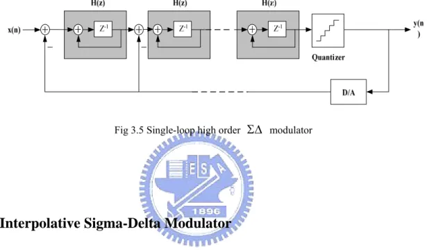
Fig. 3.5 is a single loop high order ΣΔ modulator, from the derivation in Section 3.1 and Section 3.2, we can get the quantization noise PQ in signal bandwidth is as
PQ = 2L 1 L 2 2 LSB ) OSR 1 ( 1 L 2 12 V ⋅ + + ⋅ π ,L:order (3.14) and its PSNR is PSNR = 6.02B+1.76-10 log( 1 L 2 L 2 + π )+(20L+10) log(OSR) (3.15)
In the application of high order ΣΔ modulator, (6L+3)dB increases in SNR when OSR is octave, so PSNR can be raised by increasing the order of the system, especially at large oversampling ratio. But sometimes in high order architecture, the performance will be worsen than result predicted by (3.13), because of the stability problem, it will make less effective noise shaping function, so the quantization noise will not be suppressed completely.
Fig 3.5 Single-loop high order ΣΔ modulator
3.4 Interpolative Sigma-Delta Modulator
Interpolative is a kind of high order ΣΔ modulator, it changes connection of some stages, adds some feedforward paths and feedback paths in order to suppose more aggressive noise shaping effect, Fig. 3.6 is a four-order interpolative architecture ΣΔ modulator [Cha 90]. 1 1 z 1 z − − − 1 1 z 1 z − − − 1 1 z 1 z − − − 1 1 z 1 z − − −
This architecture also has stability problem, when the order L increases, each integrator produces one pole, and when the order is higher, poles of this system will also increase, and it will cause unstable situation, so the range of integrator gain will be limited; if the range of integrator gain is small, oscillation will appear in the circuits. Another is the considerations of clock control, when we use SC (switched-capacitor) to implement the integrator, each integrator needs two clocks to control its operation, and we will need more clock to control the integrator when the order of system increases, it will produce more problems.
3.5 MASH Architecture
MASH (Multi-stage noise shaping) architecture is also called cascade architecture, which is a method that cascades several low order loops modulator in order to get high order noise shaping effect. The fundamental ideal of MASH is delivering quantization noise of front stage to input of next stage, and combining the digital outputs of all the stages with proper transfer function in digital domain, only the quantization noise of last stage will appear at the output, and the orders of NTF is the same with total orders in the cascade ΣΔ modulator. Fig 3.7 is a
three-order cascade ΣΔ modulator, its is the combination of a second-order and first-order ΣΔ modulator, so also called 2-1 cascade architecture [Wil 94].
1 − Z 1 − Z Z−1
Fig. 3.7 2-1 architecture MASH ΣΔ modulator
From Fig. 3.7, we can derive the first stage output Y1(z) can be represented as
Y1(z) = z-2X1(z) + (1-z-1)2E1(z) (3.16)
Output of second stage Y2(z) is as
Y2(z) = z-1X2(z) + (1-z-1)E2(z) (3.17)
and overall output of MASH Y(z) is as
Y(z) = H1(z)Y1(z) + H2(z)Y2(z) (3.18)
and we can say that second stage input X2(z) is almost the same with E1(z), in order to
eliminate first stage quantization noise E1(z), from (3.16) ~ (3.18), we can define the error
H1(z) = z-1 (3.19)
H2(z) = (1-z-1)2 (3.20)
From (3.16)~(3.20), E1(z) can be eliminated, and second stage quantization noise E2(z) is
shaped by third-order noise shaping function, and the MASH output Y(z) is as
Y(z) = z-3X1(z) + (1-z-1)3E2(z) (3.21)
The most significant advantage of this architecture is that stability is not an issue, because it is composed by several low-order systems, and the quantization noise will not be amplified stage by stage, so its stability is good. Most important, the noise shaping function is equivalent as high order ΣΔ modulator, so it is popular in recent publications [Rio 04][Vle 01]. However, there also have some drawbacks of this topology; it is sensitive to the circuits' imperfections, such as finite DC gain of OTA, variance of integrator gain due to capacitor mismatch and non-zero switch resistance. These are all practical considerations when we design a MASH architecture ΣΔ modulator [Gag 03].
3.6 Multi-bit Quantizer Sigma-Delta Modulator
The demands of high resolution and high bandwidth ADC are more and more in recent years. In a high signal bandwidth, OSR of ΣΔ ADC can’t be too high, and the peak SNR of a ΣΔ modulator with such limited OSR can’t satisfy of high resolution applications, if we use higher order architecture, then the performance will degrade due to instability. So the most general method to increase performance is to use multibit quantizer. The most obvious advantage of using multibit quantizer is that the distance between quantizer level VLSB in (2.4)
is much smaller due to increasing of B, and according to (2.3), the power of quantization noise is attenuated. Fig. 3.8 is the results of theoretical peak SNR of ΣΔ modulator versus oversampling ratio, with different order and quantizer bits, it is noted that peak SNR of the same OSR is increase 6 dB with each additional bit number in quantizer, and at low OSR, low order higher bit number architecture has equivalent performance as high order architecture. This result is usable for high bandwidth applications, and the power consumption of digital circuit in ΣΔ modulator is reduced due to lower sampling rate [Pel 99].
0 50 100 150 200 250 300 20 40 60 80 100 120 140 160 OSR SN R O2B1 O2B2 O2B3 O3B1
Fig. 3.8 SNR vs. OSR with different quantizer bit number
Because of using multi-bit quantizer, so we also need to use multi-bit DAC(Digital-to Analog Converter) to transfer the digital output to analog signal, and feed it back to integrator. The most significant disadvantage is the non-linearities introduced by multi-bit DAC can degrade the performance of ΣΔ converter, like Fig. 3.9. It is a linear model of multi-bit ΣΔ
modulator, where E(Q) and E(D) represent the quantization noise and feedback DAC noise
respectively. The values of these capacitor elements in DAC will not equal to ideal values that we need, it is due to process variation, typical value of mismatch in modern CMOS technology is about 0.05% ~ 0.5%. In recent years, so many researches are make efforts on reduce DAC noise due to mismatch, such as trimming [Nor97], Dynamic element matching(DEM)[Mil 03][Reb 90], although trimming is effective, but it has a expensive production step. So, DEM becomes more and more popular because of its efficiency and cheaper cost.
Fig. 3.9 Multi-bit architecture
3.7 Multi-bit Sigma-Delta Modulator use DEM Technique
Dynamic element matching is a different approach to decrease the DAC noise, it is used to improve the linearity of pure DACs [Pla 79], but now it is most used in inner DAC of multi-bit ΣΔ modulator. A DAC with DEM technique is illustrated in Fig. 3.10, 2 bits B
thermometer code is put into the element selection logic block, and the function of element selection logic is try to select DAC elements in such way let the errors introduced by DAC average to zero for several operation periods. Because the DEM block is located in feedback loop, so its delay must be very small prevent to degrade the performance of ΣΔ converter, therefore the algorithm used in the DEM block must be simple. There are several techniques of DEM, such as Randomization [Car 89], Clocked Averaging (CLA) [Pla 79], Individual Level Averaging (ILA) [Che 95], Data Weighted Averaging (DWA) [Bai 95], Randomization
is the first approach to use DEM technique in ΣΔ ADC, and DWA offers a good
performance to reduce DAC error, in this section, an overview introduction of these two algorithms will be presented, and the operation principle of them will be explained.
1 2B− 1 2 B 2 B 2
Fig. 3.10 A B-bit DAC with DEM technique
3.7.1 Randomization Technique
The main operation principle of randomization is that the element selection logic performs as a randomizer. In each clock period, the randomizer selects DAC elements randomly to generate the output of DAC. If the randomizer is ideal, then the DAC noise will become uncorrelated with each other. Simulation results show that randomization DEM
technique reduces the noise floor from DAC error by several dB, but it still be a white noise in low frequency. Fig. 3.12 is the output spectrum of a second-order ΣΔ modulator with a 0.1% capacitor mismatch, it is notable that the noise floor of randomization DEM is lower than that without any calibration technique in the feedback DAC.
3.7.2 Data Weighted Averaging (DWA)
DWA is a efficiently method to reduce DAC mismatch noise, it uses one register to remember the capacitor last time used, and always points to the first unused unit capacitor in this clock, so DWA rotates through all the unit capacitors such that all capacitors are used at the maximum possible rate. From this algorithm, each elements is used the same number of times in long interval, this ensures that the errors caused by the DAC average to zero quickly. In Fig. 3.11, it is a 4-bit DAC and the shaded boxes are the number of 1’s in the thermometer code. Assumes that the input codes sequence is 8, 8, 10, 9, 10, 10, 11, 11, 12, 11, 14, 11, 14, 13, 12, 15... Fig. 3.12 is the simulation results of a third order ΣΔ modulator, we can see that without DEM has highest noise floor and DWA works as a first order noise shaping function of DAC noise, ideal DAC only with quantization noise has third-order noise shaping.
10-3 10-2 10-1 -200 -180 -160 -140 -120 -100 -80 -60 -40 -20 0 60 dB/decade PS D Normalized Frequency No DEM DWA ideal DAC
Fig. 3.12 Output spectrum with three kinds of DAC
Another consideration is the sub-ADC(quantizer) of the ΣΔ modulator, we usually use Flash A/D as the multi-bit quantizer because of its high speed, but Flash A/D has a significant disadvantage is that the number of comparators of it is proportional to 2B. That means a 6 bit quantizer needs 64 comparators, the occupied area of comparator may not much, but in modern SOC applications, the problems of power and area are important, so it becomes one limitation of multi-bit quantization.
ΣΔ A/D converter is attractive for high resolution application, for higher signal bandwidth, we increase system order to raise SNR, but it still have stability problem. So people develop MASH and multi-bit architecture to improve its performance. Finally, we classify they into low order, high order, MASH and multi-bit four kinds of architecture, and compare their advantage and disadvantage as Fig. 3.13 [Med 99]
ΣΔ
Fig. 3.13 Comparison of ΣΔ modulator architectures
3.8 Decimator
In ΣΔ A/D converter, digital decimator is used to process digital signal of the quantizer output, the high speed data word after oversampling modulation can’t be used directly. Because there have original signal and quantization noise among it, so the main function of decimator is to convert the oversampled B-bit output words of the quantizer at a sampling rate of fs to N-bit words at Nyquist rate of input, and removes the noise out of signal band. In order to prevent the noise introduced by other frequency, the decimator filter must have very flat signal pass-band, and sharp transition region and enough signal attenuation in stop band. Two-stage decimator is used in a general situation, because that single stage decimator is difficult to convert sampling rate to Nyquist rate in 1 time and without degrading SNR. In the
first stage, we can down-sample the sample frequency to 2~4 times of Nyquist frequency, and in the second stage, we can use IIR or FIR filter that have high linearity [Nor 97]. For a large OSR, multi-stage decimator is used.
3.9 Performance Metrics for a
ΣΔModulator
In order to understand the performance merits used to specify the behavior of ΣΔ modulator, several specifications concerning the performance are discussed [Gee 02].
․Signal to Noise Ratio: The SNR of a data converter is the ratio of the signal power to the noise power, measured at the output of the converter for a certain input amplitude. The maximum SNR that a converter can achieve is called the peak SNR.
․Signal to Noise and Distortion Ratio: The SNDR of a converter is the ratio of the signal power to the power of the noise and the distortion components, measured at the output of the converter for a certain input amplitude. The maximum SNDR that a converter can achieve is called the peak SNDR.
․Dynamic Range at the input: The DRi is the ratio between the power of the largest input
signal that can be applied without significantly degrading the performance of the converter, and the power of the smallest detectable input signal. The level of significantly degrading the performance is defined as the point where the SNDR is 6 dB bellow the peak SNDR. The smallest detectable input signal is determined by the noise floor of the converter.
․Dynamic Range at the output: The dynamic range can also be considered at the output of the converter. The ratio between maximum and minimum output power is the dynamic
range at the output DRo, which is exactly equal to peak SNR.
․Effective Number of Bits: ENOB gives an indication of how many bits would be required in an ideal quantizer to get the same performance as the converter. This numbers also includes the distortion components and can be calculated from (2.6) as
02 . 6 76 . 1 ENOB= SNR− (3.22)
․Overload Level: OL is defined as the relative input amplitude where the SNDR is decreased by 6dB compared to peak SNDR
Typically, these specifications are reported using plots like Fig. 3.14. This figure shows the SNR and SNDR of the ΣΔ converter versus the amplitude of the sinusoidal wave applied to the input of the converter. For small input levels, the distortion components are submerged in the noise floor of the converter. Consequently, the SNDR and SNR curves coincide for small input levels. When the input level increases, the distortion components start to degrade the modulator performance. Therefore, the SNDR will be smaller than the SNR for large input signals. Note that these specifications are dependent on the frequency of the input signal and the clock frequency of the converter. Fig. 3.14 also shows that SNDR curves drop very fast once the overload point is achieved. This is due to the overloading effect of the quantizer which results in instabilities.
Chapter 4
Models of Multi-Bit Sigma-Delta Modulator
Power
The power estimation is presented for a sigma-delta converter with a certain accuracy and bandwidth specification. The influence of several design choices on the power-bandwidth-resolution trade-off will be discussed. This leads to some general design considerations.
The power estimation can be derived into the analog power consumption and the digital power consumption. The analog power consumption mainly includes the OTA of the integrator, the comparator of the quantizer, and the DAC from the quantizer to the integrator. The digital power consumption mainly includes the logic in the quantizer, the dynamic element matching algorithm, the CMOS switch and the clock generator. But in this paper, the digital power consumption only considers the CMOS switch and the clock generator.
4.1 Integrator power
The first considered power consumption is the integrator of the analog power consumption. The most power consumption is the OTA in the integrator. So, the total power consumption of the OTA can be written as
OTA OTA DD
OTA B DD
k I V
= ⋅ ⋅ (4.1)
where IOTA represents the total current of the OTA, IB represents the bias current of the OTA, kOTA represents the ratio of the total current of the OTA to this bias current and VDD
represents the supply voltage of the OTA. The factor kOTA which depends on the number of current branches and the relative amount of current in each of them.
The ratio of the total current of the OTA to this bias current is represented by
2 1 2 B OX eff W I C V L μ = ⋅ ⋅ ⋅ ⋅ (4.2) Where Veff = VGS−VTH
For CMOS implementations, the OTA transconductance is related to the transconductance of a MOS transistor used in a differential input pair. The transconductance of the OTA to current relationship for a differential input pair is given by
2 B m OX eff eff I W g C V L V μ = ⋅ ⋅ ⋅ = . (4.3) So IB can be written as 1 2 B m eff I = ⋅g V⋅ (4.4)
where IB represents the bias current of each transistor of the differential pair and Veff
represents the overdrive voltage.
, 1 P L 1 S 1 P eq cl S S S I S C C C C C C C C C C ⎛ ⎛ ⎛ ⎞⎞⎞ = ⋅ +⎜⎜ + ⎜⎜ + ⎜ + ⎟⎟⎟⎟⎟ ⎝ ⎠ ⎝ ⎠ ⎝ ⎠ , Ceq cl S k C = ⋅ (4.5)
where kCeq cl, represents the ratio between the effective closed-loop load capacitance and the sampling capacitance. It depends on the relative size of CP and CL compared to CS. These sizes can only be determined when the OTA is designed since they depend on parasitic capacitances. The ratio of CS to CI is determined by loop-coefficient a1 of the sigma-delta converter[Gee 02].
The gain-bandwidth product of operational amplifier of the first integrator is a function of the equivalent load capacitor Ceq cl, and of the transconductance
g
m, according to2 , , 2 2 m m cl eq cl Ceq cl S g g f C k C π π = = i i i . (4.6)
The bias current of each transistor of the differential pair combined the gain-bandwidth product of operational amplifier with the equivalent load capacitor, so IB can be written as
1 2 B m eff I = g V⋅
(
)
2 , 1 2 2 fcl π kCeq cl CS Veff = i ⋅ ⋅ ⋅ ⋅ , 2 Ceq cl S eff cl k C V f π = ⋅ ⋅ ⋅ ⋅ (4.7)be written as OTA OTA DD P =I ⋅V OTA B DD k I V = ⋅ ⋅
(
, 2)
OTA Ceq cl S eff cl DD
k π k C V f V
= ⋅ ⋅ ⋅ ⋅ ⋅ ⋅
, 2
OTA Ceq cl S cl eff DD
k k C f V V
π
= ⋅ ⋅ ⋅ ⋅ ⋅ ⋅ (4.8)
The power consumption of the first integrator is almost consumed in the first OTA. So this equation can be extended to the total analog power consumption of all the integrators in a sigma-delta converter by introducing the factor kΔ ∑ which represents the ratio between the total current consumption of all the OTAs and the first OTA. The total analog power consumption of the integrators in a sigma-delta converter is given by
an DD P =IΔ ∑⋅V OTA DD kΔ ∑ I V = ⋅ ⋅ , 2
OTA Ceq cl S cl eff DD
k k k C f V V
π Δ ∑
= ⋅ ⋅ ⋅ ⋅ ⋅ ⋅ ⋅ (4.9)
The analog power consumption is not included the power consumption of the quantizer yet.
OTA
k indicates how much current the OTA consumes, relative to the bias current of one transistor of the differential input pair. This depends on the chosen OTA architecture. Three different alternatives are now briefly compared.
A single-stage telescopic OTA is shown in the Figure 1[Kus 98]. It can provide a large gain, has an excellent frequency performance and has only two current branches. This means
OTA
k is only two. The mean drawback is the small output swing since it has five stacked transistors which have to remain in saturation region. Furthermore, it becomes difficult to employ the same common-mode levels at the input and the output of the OTA.
Figure 4.1 A single-stage telescopic OTA
The folded cascode OTA is shown in the Figure 2[Kus 98]. It can provide a large gain, and has an excellent frequency performance. The frequency performance of the folded cascade OTA is worse than the frequency performance of the telescopic OTA because more parasitic capacitances are associated with the non-dominant pole. The folded cascode OTA has two current branches that resulting in a value of four for kOTA.
Compared with the telescopic OTA, the main advantages of the folded cascade OTA are the large output swing and the larger range for the input common-mode level. Because the folded cascode OTA only has four transistors need to remain in saturation.
Figure 4,2 The folded cascode OTA
The two-stage Miller-compensated OTA is shown in the Figure 3[Kus 98]. It also can provide a large gain, but the frequency performance is worse. The dominant pole is determined by the compensation capacitance. The non-dominant pole is determined by the ratio of the transconductance of the output stage to the load capacitance. Compared with the telescopic OTA and the folded cascade OTA, the kOTA of the two-stage Miller-compensated OTA is difficult to get it. Because the two-stage Miller-compensated OTA must improve the frequency performance by the compensation capacitance. The transconductance of the two-stage Miller-compensated OTA to current relationship for a differential input pair is
1 1 1 2 B m GS T I g V V = − . (4.10)
And, the bandwidth of the two-stage Miller-compensated OTA to transconductance relationship for a differential input pair is
1 2 2 m cl M g f C = π⋅ (4.11)
where CM is the Miller compensation capacitance.
So, the bandwidth of the two-stage Miller-compensated OTA to current relationship for a differential input pair is
(
)
1 1 1 1 2 B m GS T I = g ⋅ V −V 1 2 2(
1)
2 π fcl CM VGS VT = ⋅ ⋅ ⋅ ⋅ − = ⋅π fcl2⋅CM ⋅(
VGS1−VT)
. (4.12)The non-dominant pole, which is created by the load capacitance, should be placed beyond the three times of the fcl2[Lib 04]. This criterion is shown as
3 2 , 3 2 m cl M eq cl g f C +C = ⋅ π⋅ =6π⋅fcl2. (4.13)
So, the bandwidth of the two-stage Miller-compensated OTA to the branch current relationship is
(
)
3 3 3 1 2 D m GS T I = g ⋅ V −V 1 6 2(
,)
(
3)
2 π fcl CM Ceq cl VGS VT = ⋅ ⋅ ⋅ + ⋅ − = ⋅π fcl2⋅(
3CM +3Ceq cl,)
⋅(
VGS3−VT)
. (4.14)In general design of the operational amplifier, the phase margin usually is about60 . 0 Assuming that a 60 phase margin is required, the following relationships apply[Phi 02]: 0
, 0.22 M eq cl C ≥ C . (4.15) Let 3 1 GS T GS T V −V =V − . V (4.16)
Therefore, the bandwidth of the two-stage Miller-compensated OTA to current relationship for a differential input pair is also written as
(
)
1 2 1
B cl M GS T
I = ⋅π f ⋅C ⋅ V −V
=0.22π⋅ fcl2⋅Ceq cl, ⋅
(
VGS1−VT)
. (4.17)And, the bandwidth of the two-stage Miller-compensated OTA to the branch current relationship is also written as
(
)
(
)
3 2 3 3 , 3 D cl M eq cl GS T I = ⋅π f ⋅ C + C ⋅ V −V = ⋅π fcl2⋅ ⋅(
3 0.22Ceq cl, +3Ceq cl,)
⋅(
VGS1−VT)
=3.66π⋅ fcl2⋅Ceq cl, ⋅(
VGS1−VT)
. (4.18)Consequently, the total currents of the two-stage Miller-compensated OTA can be written as
2 2
= ⋅2 ⎣⎡π⋅fcl2⋅CM⋅
(
VGS1−VT)
⎦⎤+ ⋅2 ⎡⎣π⋅ fcl2⋅(
3CM +3Ceq cl,)
⋅(
VGS3−VT)
⎤⎦= ⋅2 0.22⎡⎣ π⋅fcl2⋅Ceq cl, ⋅
(
VGS1−VT)
⎦⎤+ ⋅2 3.66⎣⎡ π⋅fcl2⋅Ceq cl, ⋅(
VGS1−VT)
⎤⎦=7.76π⋅ fcl2⋅Ceq cl, ⋅
(
VGS1−VT)
. (4.19)This means kOTA is only 7.76 for the two-stage Miller-compensated OTA.
Figure 4.3 The two-stage Miller-compensated OTA
kΔ ∑ represents the ratio between the total current consumption of all the OTAs and the first OTA. At first sight, one would expect that it increases significantly as the order of the converter increases since an extra OTA is required.
,
Ceq cl
k represents the ratio between the effective closed-loop load capacitance and the sampling capacitance.
4.2 Quantizer power
A multi-bit quantizer is used to quantize the analog signal to multi-level digital output signal in the implementation of a multi-bit sigma-delta modulator. The multi-bit quantizer is implemented by Nyquist-rate analog to digital converter. In the multi-bit sigma-delta modulator, the power estimation for the quantizer can be as the power estimation for the Nyquist-rate ADC. There are many parameters to be considered for the quantizer (Nyquist-rate ADC) like the speed and the accuracy.
The power is proportional to the supply voltage, the frequency and a charge. And, the power can be wrote as
Charge
DD DD
P V= ⋅ =I V ⋅ ⋅f . (4.20)
From the equation (20), we can find a question. The question is what frequency should be considered for the multi-bit quantizer and then which charge is being transferred. The quantizer has two parts, comparators and processing circuitry. The comparator is clocked at frequency of the sample and the processing circuitry varies at the frequency of the input signal. So the equation (1) can be wrote as [Eri 02]
, sin _ ,
comparator fs proces g circuit fb
P P= +P . (4.21)
and
(
)
DD
P V= ⋅ ⋅f Voltage swing C⋅ . (4.22)
The voltage swing for the comparators is always the full supply voltage. So the equation (22) can be wrote as
2
DD
P V= ⋅ ⋅ . C f (4.23)
About the capacitances is not easy to estimate in the quantizer. Therefore, the equality is replaced by a proportionality and the capacitance is taken proportional to the technology’s minimal channel length. So the following equation for the total power estimator is [Eri 02]
(
)
2 min
DD
P V∝ ⋅L ⋅ fs+ fb . (4.24)
The accuracy is expressed as the effective number of bits (ENOB), which is defined as shown in the well-known [Eri 02]
(
)
20 log 1.76
6.02
SNDR
ENOB= ⋅ − . (4.25)
where SNDR represents the signal-to-noise-and-distortion ratio. The accuracy expressed in (6) is related to the size of the devices and in this way to the power (5): this correlation has been investigated for 75 data points as show in Figure 4 [Eri 02]. From the Figure 4, we can get the following regression relation[Eri 02]
(
)
2 min log DD 0.1525 4.8381 Q V L fs fb ENOB P ⎛ ⋅ ⋅ + ⎞ = − ⋅ + ⎜ ⎟ ⎜ ⎟ ⎝ ⎠ . (4.26)So the final power estimator for the complete CMOS Nyquist-rate ADC can be written as [Eri 02]
(
)
2 min ( 0.1525 4.8381) 10 DD Q ENOB V L fs fb P = −⋅ ⋅ ⋅ ++ . (4.27)Figure 4.4.An overview of the obtained data points. The ENOB are given as a function of the input signal frequency.
4.3 DAC Power
We estimate the power consumption of multi-bit DAC in the single-loop multi-bit sigma-delta converter. The multi-bit DAC is shown in Figure 5 (a) [Gag 03]. It is composed of switches and unit capacitors. At first, we consider charge and discharge for an unit capacitor in the multi-bit DAC. The operations of a unit capacitor are illustrated in Figure 5 (b) and Figure 5 (c) respectively. We assumed that the periods of charge and discharge both are T/2, the power consumption of a unit capacitor in the multi-bit DAC is
2 0 2 1 1 (0 ) T T u Cu u T Cu u P V I dt V I dt T T =
∫
⋅ +∫
− ⋅ . (4.28)Cu u
dV
I =Cu dt. (4.29)
When (29) substitutes for Iu in (29), (28) can be derived as
2 0 2 1 1 (0 ) T T Cu Cu u Cu T Cu dV dV P V Cu dtdt V Cu dtdt T T =
∫
⋅ +∫
− ⋅ 0 0 1 1 (0 ) Vref Cu Cu Vref Cu Cu V Cu dV V Cu dV T T =∫
⋅ +∫
− ⋅(
2)
(
2)
0 1 1 1 1 = 2 + 0- 2 0 Cu Cu Vref V Cu V Cu Vref T ⋅ ⋅ T ⋅ ⋅(
2)
(
2)
1 1 1 1 = 2 Vref Cu + 0- - 2 Vref Cu T ⋅ ⋅ T ⎡⎣ ⋅ ⋅ ⎤⎦ 2 2 s 1 = ref = ref f TV ⋅Cu V ⋅Cu⋅ . (4.30)We can get the power estimation of a unit capacitor from (30), so the total power estimation for a multi-bit DAC is
2 2 2B DAC s P = ⋅ ⋅Cu Vref⋅ ⋅ f 2 1 2 2 2 B s B Cs Vref f = ⋅ ⋅ ⋅ ⋅ 2 2 Cs Vref fs = ⋅ ⋅ ⋅ . (4.31)
CI Cs Cu +Vref -Vref OTA Vin-(a)
Cu
V
Cu+
_
(b) (c)Figure 4.5 (a) Implementation of the integrator and the feedback DAC. (b) To charge the unit capacitance. (c) To discharge the unit capacitance.
4.4 Clock driver power and switch power
Static CMOS logic gates are very power-efficient because they dissipate nearly zero power while idle, so the primary dissipation component is the dynamic dissipation component.
And, the primary dynamic dissipation component is charging and discharging the load capacitance. For much of the history of CMOS design, power was a secondary consideration behind speed and area for many chips. As transistor counts and clock frequencies have increased, power consumption has skyrocketed and now is a primary design constraint.
Begin to review some definitions first. The instantaneous power P t drawn from the ( ) power supply is proportional to the supply current iDD( )t and the supply voltage VDD
( ) DD( ) DD
P t =i t V⋅ . (4.32)
The energy consumed over some time interval T is the integral of the instantaneous power.
And, the energy can be wrote as
0 ( )
T
DD DD
E=
∫
i t V dt⋅ . (4.33)The average power over this interval is
0 1 ( ) T avg DD DD E P i t V dt T T = =
∫
⋅ . (4.34)Considering an ideal inverter and a CMOS inverter with the load capacitor CL are shown in Figure 6 (a) and Figure 6 (b) respectively. Giving a periodic square-wave from the input point is shown in Figure 6 (c). The associated NMOS transistor is ON and the PMOS transistor is OFF when the input signal approach high level voltage at t = . At the same 0− time, the output voltage is 0 volts (GND).
Further, the associated NMOS transistor is OFF and the PMOS transistor is ON when the input signal voltage is changed from high level voltage to low level voltage at t=0. At the same time, the charging current pours into the load capacitor through the channel PMOS transistor, and the output voltage is going to approach high level voltage. At first, the energy of computation is E provided by the power supply is S
( ) ( ) S DD DD E =
∫
V ⋅i t dt V= ⋅∫
i t dt =VDD⋅ =Q VDD⋅(C VL⋅ DD) 2 L DD C V = ⋅ . (4.35)However, the energy E which stored up on the load capacitor is C
( ) ( ) ( ) ( ) C DD DD L dv E V t i t dt V t C dt dt =
∫
⋅ =∫
⋅ ⋅ 2 1 = ( ) 2 L DD L DD C ⋅∫
V t dv= C V⋅ . (4.36)Therefore, the energy E which dissipated on the PMOS transistor should be equal to the P
energy E provided by the power supply to subtract the energy S E stored up on the load C
capacitance, also is P S C E =E −E 2 1 2 1 2 2 2 L DD L DD L DD C V C V C V = ⋅ − ⋅ = ⋅ . (4.37)
transistor is ON and the PMOS transistor is OFF. After transformation, the load capacitor will be discharged through the channel of NMOS transistor, and leads to the power dissipation on the NMOS transistor. Consequently, the energy E which dissipated on the NMOS should N
be equal to the energy E stored up on the load capacitor, also is C
2 1 2
N C L DD
E =E = C V⋅ . (4.38)
For this reason, the total energy consumed by the logic gate in one cycle
is
(
)
2P N L DD
E +E =C Vi . If the input signal frequency of the CMOS inverter is f ,so the dynamic power dissipation PD dyn( ) is
2 ( )
D dyn L DD
P = ⋅f C V⋅ . (4.39)
(c)
Figure 4.6 (a) an ideal inverter for logic level with a load capacitance (b) an ideal CMOS inverter for transistor level with a load capacitance (c) a periodic square-wave for the input.
The switched-capacitor circuits and quantizers require various clock signals. These signals are generated on chip from one external clock signal. The switched-capacitor circuit requires two non-overlapping clocks for sampling and the integration phase. The clock generator with non-overlapping clocks is shown in Figure 2[Gee 02]. From Figure 7, it shows that the clock generator is composed of the logic gates. The primary logic gates which compose of the clock generator are inverters and the NAND gates. Assuming the clock generator has N logic gates, and the capacitance of one capacitor isC Clogic. Under these assumptions the power dissipation of the clock generator can be wrote as
2 clock clock DD P = ⋅f C ⋅V 2 log C ic DD N f C V = ⋅ ⋅ ⋅ . (4.40)
Figure 4.7 the clock generator with non-overlapping clocks.
Another important component for the power dissipation is offered by CMOS transmitters in the switched-capacitor circuits. The output of the clock generator is connected to the gate of the CMOS switches in the switched-capacitor circuits. The CMOS switch is shown in Figure 4.8. Assuming that the number of the CMOS transmission gate in Sigma-Delta modulator is NS and the gate capacitances of all CMOS transmission gates are Cgate. Under these assumptions the power dissipation of the CMOS switch can be wrote as
2 switch switch DD P = ⋅f C ⋅V 2 S gate DD N f C V = ⋅ ⋅ ⋅ . (4.41)