國 立 交 通 大 學
電子工程學系 電子研究所
碩 士 論 文
金氧半場效應電晶體在次臨界區的不匹配效應
Mismatch of MOSFETs in Subthreshold Region
研 究 生:蔡濬澤 Chun-Tse Tsai
指導教授:陳明哲 Prof. Ming-Jer Chen
金氧半場效應電晶體在次臨界區的不匹配效應
Mismatch of MOSFETs in Subthreshold Region
研 究 生:蔡濬澤 Student:Chun-Tse Tsai
指導教授:陳明哲博士 Advisor:Dr. Ming-Jer Chen
國 立 交 通 大 學
電子工程學系 電子研究所
碩 士 論 文
A Thesis
Submitted to Department of Electronics Engineering & Institute of Electronics
College of Electrical Engineering and Computer Engineering
National Chiao Tung University
in Partial Fulfillment of the Requirements
for the Degree of
Master of Science
In
Electronics Engineering
September 2010
Hsinchu, Taiwan, Republic of China
金氧半場效應電晶體在次臨界區的不匹配效應
研究 生: 蔡濬 澤 指導 教授: 陳明哲博士 國立交通大學 電子工程學系 電子研究所碩士班摘要
本論文研究隨機摻雜物以及電路的不匹配效應對於臨界電壓擾動的影響與 其物理模型。首先,我們量測各種不同尺寸的電晶體,並觀察到在次臨界區存在 比過臨界區更大的電特性誤差。接著我們萃取出許不同的製程參數,並且建立一 個有關通道摻雜濃度變異的新模型來解釋臨界電壓隨著閘極長度的縮短而上升。 同時我們發現到萃取出的臨界電壓變動值會與元件面積平方根的倒數成正比,這 與前人所提出的理論符合。我們也發現背閘順向偏壓可以減少製程參數變動值並 可用來補償小尺寸電晶體較大的參數變動值。 接著我們特別著重在進一步探討臨界電壓的擾動特性。過程中我們觀察到在 不同的汲極電壓下,所造成的臨界電壓的差異,此時因電子的能階產生變化,而 會導致元件的控制力有所升降。再來我們利用 Takeuchi 的模型做比對,並考慮 到隨機摻雜以及硼簇合族對於臨界電壓擾動的影響。從我們分析的結果看來,隨 機摻雜對於臨界電壓擾動的影響會因為硼簇合族的原子個數上升而更加明顯。在 最後,我們推導出一個在次臨界區中,與汲極電流誤差相關的新的臨界電壓擾動 模型,並且此模型能經由電流誤差成功的估計臨界電壓的擾動值。Mismatch of MOSFETs in Subthreshold Region
Student: Chun-Tse Tsai Advisor: Dr. Ming-Jer Chen
Department of Electronics Engineering Institute of Electronics
National Chiao Tung Universitty
Abstract
The physical model of the threshold voltage fluctuation from random dopant, as
well as current mismatch, is investigated in the thesis. At first we have extensively
characterize MOSFETs with different gate widths and lengths, especially in
subthreshold region of operation. We observe that the mismatch exhibits a larger
mismatch while operating in subthreshold region than in above-threshold region. We
extract various process parameters and hence construct a new model due to varying of
channel doping to explain the threshold voltage increase with gate length decrease.
The threshold voltage variations are shown to follow the inverse square rule.
Simultaneously, the back-gate forward bias is found to be able to reduce the mismatch
and compensate for larger variations for smaller devices.
Further, we pay more attention to the threshold voltage fluctuation, and observe
that the drain voltage might cause the DIBL. Then we discuss the threshold voltage
fluctuation by a Takeuchi plot, and the effect of random dopant and the boron clusters
are taken into account. From our analysis, the random dopant induced threshold
voltage fluctuation has more significant effect on threshold variation while the
number of boron atoms per cluster increases. Finally, we also statistically derive a
new model that can estimate the threshold voltage fluctuation from drain current
Acknowledgement
兩年的時間,稍縱即逝,轉眼之間,畢業的時刻已經到來。回想兩年間的日 子,充滿了許多的回憶,有歡笑,也有淚水。但是天下無不散的筵席,雖然充滿 許多不捨,但還是必須離開,邁向新的人生階段。 在此,我要感謝在這兩年之中,實驗室的大家的幫助。首先要感謝指導我的 陳明哲老師,在這兩年中,除了指導了我許多研究上的知識之外,也激發了我對 於半導體物理的興趣。同時,也以他自身的經驗,告訴我許多待人處世的道理, 使我獲益良多。再來我要感謝實驗室的學長和同學們。李建志學長在認真研究的 同時,總是不忘帶給大家歡樂的氣氛;許智育學長對於研究認真的態度,一直是 我心中的楷模;感謝李韋漢學長總是能在我研究遇到瓶頸時,給與我協助;詹益 先同學是研究上的好夥伴,總是能解答我的疑惑;鄭寬豪同學的待人處世以及研 究精神,讓我從中學習到不少;而張華罡同學總能以他幽默的風格,讓我暫時忘 卻研究過程中的枯燥。感謝實驗室的學弟妹們,因為有你們,讓實驗室增添了幾 分色彩。 我要感謝我的家人們,在這兩年默默支持著我,讓我感受到,家是最溫暖的 依靠。最後,再次感謝所有曾經幫助過我的人,沒有你們,就沒有今天的我。Contents
Chinese Abstract………i English Abstract………...ii Acknowledgement………..……….iii Contents……….iv Figure Captions………..vi Chapter 1 Introduction ... 1 1.1 Overview ... 11.2 Subthreshold Region of Operation... 2
1.3 Mismatch in Subthreshold Region ... 3
Chapter 2 Parameters of Mismatch ... 5
2.1 Experimental Subthreshold Operation ... 5
2.2 Extraction of Threshold Voltage ... 6
2.3 General Mismatch Model ... 7
2.4 Subthreshold Swing ... 7
2.5 DIBL Effect on Threshold Voltage ... 8
Chapter 3 Random Threshold voltage Fluctuation ... 10
3.1 Channel Doping Concentration... 10
3.2 Random Threshold Voltage Fluctuation... 12
Chapter 4 Mismatch Model Analysis and Modeling ... 17
4.1 Current Mismatch Model ... 17
4.2 Discussion of Current Mismatch Model ... 18
Chapter 5 Conclusion ... 20
Figure Captions
Fig. 1 The measurement ID mean and standard deviation in both subthreshold region
and above-threshold region with different back-gate biases... 24
Fig. 2 The measured drain current versus gate voltage characteristics with different
back-gate biases. ... 25
Fig. 3 Using constant current method to determine the threshold voltage in
subthreshold region. ... 26
Fig. 4 Measured mean threshold voltage with standard deviation versus the channel
length for different back-gate biases. ... 27
Fig.5 The measured subthreshold swing versus gate length for different gate widths.
... 28
Fig. 6 Measured mean threshold voltage versus L for different channel widths for
Vds 1V . ... 29 Fig. 7 The measured DIBL standard deviation versus the inverse square root of the
device area. ... 30
Fig. 8 The measured DIBL standard deviation versus the inverse square root of the
device area………....31 Fig. 9 The measured and calculated V standard deviation versus the inverse th1
square root of the device area. ... 32
Fig. 10 The schematic drawing of halo doping device.
..………33 Fig. 11 The flat band voltage versus channel width at L=1m. ... 34
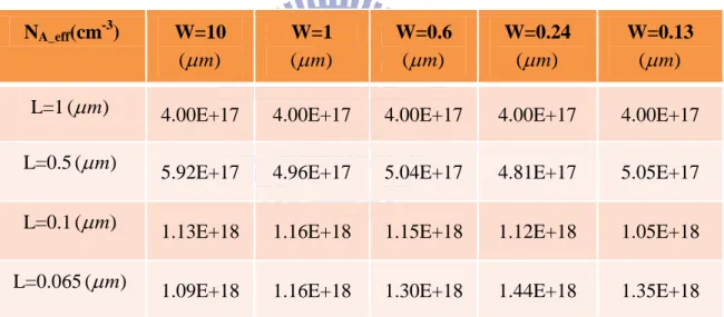
Fig. 12 The extracted NA eff_ of all device sizes.
... 35
Fig. 13 Comparing of the Vth extracted from NA eff_ and the experimental data.
... 36
Fig. 14 Using measured data based on the fluctuation model to show the results
of all device sizes for different back-gate biases. ... 37
Fig. 15 The measured standard deviation of threshold voltage difference versus
the inverse square root of the device area for different back-gate biases….38
Fig. 16 The calculated Vth dopant, versus the inverse square root of the device
area for different back-gate biases. ... 39
Fig. 17 The extracted Vth others, versus the inverse square root of the device area for different back-gate biases. ... 40
Fig. 18 The Vth dopant, with different number of boron atoms per cluster versus the inverse square root of the device area for zero back-gate bias. ... 41
Fig. 19 The Vth others, with different number of boron atoms per cluster versus the inverse square root of the device area for zero back-gate bias…………...42
Fig. 20 The experimental data and fitting line from the drain current and threshold
voltage mismatch model. ... 43
Fig. 21 The standard deviation of threshold voltage from model and experiment.
... 44
Fig. 22 The schematic flowchart for the procedure used in our works.
Chapter 1
Introduction
1.1 Overview
As the feature size of integrated MOSFET’s is decreasing, the mismatch has
gathered great importance in recent years. In order to achieve steady lowering of the
supply voltage, reducing the power consumption while holding the reliability of the
device, will lead to the worsened mismatch of device characteristic. Because of this,
there are some researches concerning the mismatch of MOSFETs in subthreshold
region [1],[2]. Even if the lithographic dimensions and layer thicknesses are well
controlled, there are still having many factors that will lead to significant variations in
the threshold voltage and drive current. In general, the designers might increase the
device area to improve the matching of the device. But this method is opposite to the
technology trends and will cause disadvantages. If the conservative transistor
geometries are used, the consequence is a waste of area, while increasing the circuit
capacitances. Therefore increases the circuit power consumption and degrades the
speed specifications. However, using reduced transistor geometries cab produce large
deviations in the transistor electrical parameters. Therefore, a precise mismatch
characterization as a function of transistor area is necessary for optimizing the
trade-offs between the area, speed, power consumption, and noise and precision in
circuit design. How to obtain balanced between them is worth discussing.
In this work, a large number of statistical data then yields the standard deviation
and mean of the distribution for random variables. For example, we can obtain the
the subthreshold swing, and the effective channel doping concentration. It can be
found that threshold voltage mismatch follows inverse square root of area. The
forecast threshold voltage fluctuations have been experimentally confirmed for a wide
range of fabricated and measured MOSFET’s down to the nanoscale region. The performance and yield of the corresponding systems may be seriously affected in the
presence of these fluctuations. Thus, we generate different mismatch models for
subthreshold region in terms of the subthreshold current and threshold voltage. All the
results will be revealed in the following chapters.
1.2 Subthreshold Region of Operation
Traditionally, the operation of MOSFETs utilizes the above-threshold region,
especially the saturation region. In the saturation region, MOSFET is considered as
the gate-controlled current source, and the current is essentially independent of the
drain voltage. But when operated in subthreshold region, the drain voltage may have
effect the current obviously. Subthreshold MOSFET conduction first attracted
attention as the leakage current in several decades before [1]. The subthreshold
conduction of MOSFET can also be used as the fundamental element for micropower
integrated circuits in early eighties [2].
In recent years, how to reduce the power consumption becomes very important
as the transistor density continuously grows in VLSI technology. Thus the
subthreshold operation of MOSFET is becoming increasingly interesting because of
the low power consumption. Following are the advantages of the MOSFET operating
in subthreshold region:
(i) Extremely low power consumption.
(iii) Exponential dependence of drain current on gate voltage.
In this thesis, we explore some characteristics of MOSFET operating in subthreshold
region, and discuss the mismatch of parameters such as threshold voltage, drain
current and drain induced barrier lowering. And we will also focus on the fluctuation
of the threshold voltage.
.
1.3 Mismatch in Subthreshold Region
It is well known that there are no two things identical in the world. This is the
case for MOSFETs. Even in the same size, there are no two transistors that are
identical because of the variation of manufacturing process. Pelgrom [4] pointed out
that the mismatch of MOSFET is proportional to the inverse square root of gate area
and are proved experimentally. Therefore, as the dimension of semiconductor device
continues to be reduced with today’s technology, mismatch becomes more and more
important. From the research works of [5] ,we can clearly know that back-gate bias
has a very huge relation with current mismatch and the back-gate forward bias can
suppress it. Thus we should simultaneously take both device area and back-gate bias
into account during the mismatch analysis.
As we mentioned above, one of the advantages of subthreshold region is the
exponential dependence of drain current on gate voltage. But on the contrary, this
relation is also to cause the large mismatch especially in the small device. Different
from the dependencies following the square rule for operating in above-threshold
region, the subthreshold region of operation has the exponential dependencies on
process parameters. Therefore, it is expected that drain current exists larger mismatch
in subthreshold region than that in the above-threshold region as shown in Fig 1.
while our parameters will be based on threshold voltage, drain-induced barrier
lowering and subthreshold swing are included. In order to reduce the mismatch
effectively, we can operate the device with back-gate forward bias applied. So, with
the device area decreasing, the mismatch increasing can be compensated by the
back-gate forward bias. This characteristic will make the subthreshold operation
Chapter 2
Parameters of Mismatch
2.1 Experimental Subthreshold Operation
The measurement of mismatch for identical devices was achieved in terms of the
dies in wafer. In this thesis, we used the measured capacitance-voltage(C-V) curve
fitting by Schred simulator to obtain the parameters due to the manufacturing
processes. They are: gate oxide thickness is 1.27nm , n+ doping concentration is
20 3
1 10 cm and the substrate doping concentration is 4 10 cm 17 3. All dies on wafer contain many n-channel MOS transistors with the same structure. All of them
were fabricated using a 65nm CMOS process. The devices under study were
n-channel MOSFETs with varying gate widths ( W =0.13 m , 0.24 m , 0.6 m , 1 m , 10 m ) and mask gate lengths ( L =0.065 m , 0.1 m , 0.5 m , 1 m ).
In our measurement, the p-well-to-n+-source bias V was fixed with the gate BS
voltage sweeping from 0 V to 1.2 V in a step of 25 mV. The drain current was
measured and recorded for subsequent analysis. All the procedure was performed
under four different back-gate bias: -0.8 V, -0.4 V, 0 V, and 0.4 V, the same as which
applied in [5]. In order to make sure of the action of the gate lateral bipolar transistors,
the choice for maximum forward bias is equal to 0.4 V. The drain voltages that we
chose are two values, one is fixed at 0.01 V in the subthreshold region, and the other
value is 1 V for extracting the drain-induced barrier lowering.
The measurement setup contains the HP4156B and a Faraday box which is used
for shielding the test wafer. All were performed in an air-conditioned room with the
inversion region. Fig. 2 displays typical measured I-V characteristics with back-gate
bias parameter on a single n-channel MOSFET.
2.2 Extraction of Threshold Voltage
There are many electrical parameters in modeling of MOSFETs. The most
important is the threshold voltage V . In general, threshold voltage may be th
understood as the gate voltage for the transition from weak inversion to strong
inversion region in the MOSFET’s channel. The threshold voltage can be extracted
from the capacitance-voltage (C-V) curve or the drain current versus gate voltage
characteristics. While the latter method is quite common to be used, there are various
methods to extract threshold voltage [6] and they have been given several distinct
definitions.
In order to extract the threshold voltage in subthreshold region, we choose the
constant current method to extract the threshold voltage in this thesis. The constant
method evaluates the threshold voltage as the value of the gate voltage, corresponding
to a given constant drain current measured at drain voltage less than 100mV. A typical
value [7] for this constant drain current is m 10 ( )7
m W A L
, where W and m L are m
the mask channel width and channel length. The threshold voltage can be determined
with voltage measurement as shown in Fig. 3. From Fig. 3, we can observe there are
large sample number (2000) used in measurement. All threshold voltages we extracted for this chosen current are from the subthreshold region. The threshold
voltage values of all device sizes we obtained by constant current method are shown
2.3 General Mismatch Model
The mismatch parameters of a group of equally designed devices are the result of
several random processes encountered during the fabrication phase of the devices.
According to [3], the standard deviation f x y( , ) of a function f x y
,
with two random variables x and y can be expressed as
2 2 2 2 2 ( , ) 2 , f x y x y ov f f f f C x y x y x y (1)where x and y are the variances of x and y, respectively; and the Cov
x y,
is the correlation coefficient between x and y. For three random variables x , y and z, the standard deviation of the distribution can also be presented in a similar
way.
We should make sure the existence of the relationship between different
parameters while using this model. If there is no correlation between each other, we
can get the simplest formula for the mismatch model. So, we need to confirm the
parameters are independent every time we want to build a new mismatch model. But
we all know that everything in the world may affect each other. In the following
chapters, we will use Eq. (1) as the threshold voltage fluctuation model, and the
correlation coefficient may be negligible due to the weak relation between different
parameters in our mismatch model.
2.4 Subthreshold Swing
In order to evaluate the value subthreshold leakage current, subthreshold swing is
defined as the gate voltage variation per decade of current. It is found from [8]:
( ) 0 GS th V V q kT n d I I e (2)
2.3 log GS d V kT S n I q (3)
where 1/ n is the fraction of (VGS Vth) that affects the source-channel barrier and
the thermal voltage kT 0.0259V
q at room temperature. The ideal value of
subthreshold swing is 60mV decade for n is equal to / 1 . The results of subthreshold swing extracted from experimental data are shown in Fig. 5. The
extracted subthreshold swing will be used in following chapter.
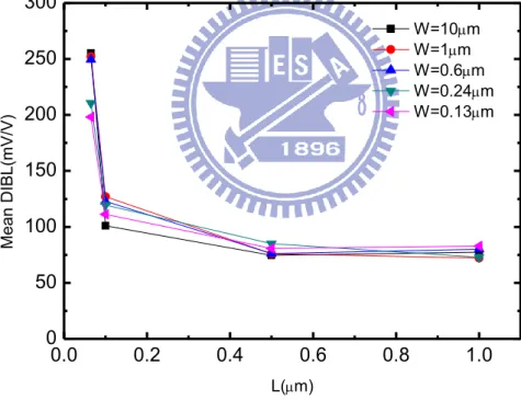
2.5 DIBL Effect on Threshold Voltage
As the advance in technology, channel length is scaling down. It is gradually
important to consider short-channel effect and drain-induced barrier lowering (DIBL).
Here we focus on the DIBL effect. In order to further discuss the DIBL, we derive a
mismatch model of DIBL as a parameter of threshold voltage fluctuation. In this work,
we use constant current method to determine the threshold voltage for large drain
voltage.
DIBL is defined as the threshold-voltage shift divided by the drain voltage
change. It can be expressed as:
1 1 0 0 1 0 ( ) ( ) th d th d d d V V V V DIBL V V (4)
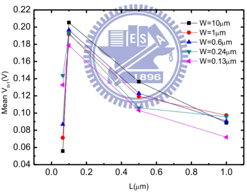
where Vth1(Vd1) is the threshold voltage extracted under Vd 1Vshown in Fig. 6, and
0( 0)
th d
V V is designated as V ,which is the threshold voltage extracted under th
0.01
d
V Vas shown in Fig. 4. With these two parameters, we can obtain the DIBL. The extracted DIBL is shown in Fig. 7.
For using the DIBL we extracted to examine the mismatch model, we write Eq. (4) as
another form:
1 ( 0 1)
th d d th
According to Eq. (1) and Eq. (5) and assume the correlation is negligible, we can
derive the mismatch model:
1 2 2 2 2 0 1 Vth d d DIBL Vth V V (6) where Vd0Vd1 0.99V in our case. Similarly with the threshold voltage standarddeviation, the DIBL standard deviation also has inverse relation of the device size as
shown in Fig. 8. Fig. 9 demonstrates the experimental data and the calculated results
of the model, where we can observe that the results are as anticipating as we can infer.
Thus we can write the standard deviation of DIBL as a function of threshold voltage
Chapter 3
Random Threshold Voltage Fluctuation
3.1 Channel Doping Concentration
Along with the advanced technology, device size is more and more small.
Channel doping concentration becomes an essential parameter of MOSFET. From
threshold voltage we display before, we observed when the channel length gets
shorter, the threshold voltage might become larger. Contrary to the short channel
effect, it is widely known that heavy channel doping may increase the threshold
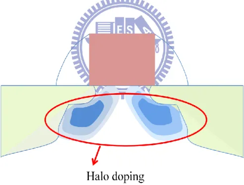
voltage. Consequently, we consider that the halo doping (near the source/drain and
under the inversion channel) will affect the effective channel doping concentration
_
A eff
N
to bring about this phenomenon. The schematic drawing of halo doping
device is shown in Fig. 10.
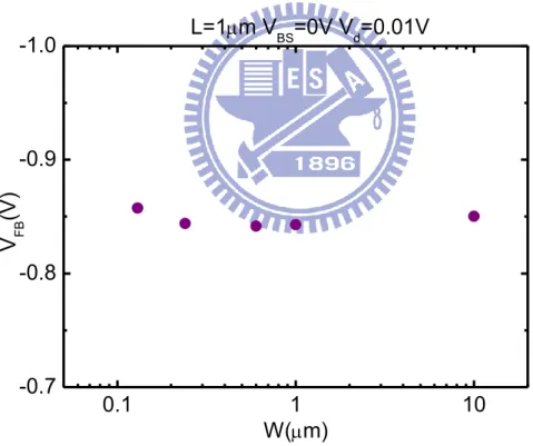
In order to find the effective channel doping concentration of our experimental
data, we start at finding the flat band voltage VFB. The flat band voltage is defined as
the gate voltage at zero band bending. From semiconductor physics studied, we
understand that the existence of many kinds of traps may affect the flat band voltage,
such as oxide trap, interface trap and fixed oxide charge. It is difficult for us to
quantify each of them. Because of this, we attempted to use the threshold voltage we
have extracted from constant current method to obtain the flat band voltage including
the trap effect.
First, the formula of threshold voltage can be derived as:
2 2
th FB f f BS
ln A f i kT N q n (8) 2 ox si A ox t q N (9) where f is the Fermi level, N is the effective well doping concentration, A n is i
the intrinsic concentration of silicon, t is the oxide thickness, and ox si and ox
are the silicon and oxide permittivities, respectively. Here we assume that flat band
voltage does not change with gate length, and the channel doping concentration of
long channel effect by halo doping can be negligible. Thus we can use the extracted
threshold voltage from five different gate widths (W =0.13 m , 0.24 m , 0.6 m , 1 m , 10 m ) at longest gate length ( L =1 m ) and N =A
17 3
4 10 cm and according to Eq. (7) to obtain five different flat band voltages with corresponding gate widths.
The extraction result is shown in Fig. 11.
Next, with the flat band voltage we have extracted and the threshold voltage of
other gate lengths ( L =0.065 m , 0.1 m , 0.5 m ), similarly, according to Eq. (7), we can obtain the effective channel doping concentration NA eff_ of different gate
lengths as shown in Fig. 12. In order to confirm if NA eff_ we extracted is reasonable,
we substituted them into the Eq. (7) for different back-gate bias to derive the
corresponding threshold voltage, and then compared the results with the experimental
data. As a result, we find that they almost match the experimental data as shown in
Fig. 13.
Although these effective channel doping concentrations we extracted may be not
the real doping concentration of the MOSFETs, but it can reveal the characteristics of
equivalent channel doping concentration of our devices.
3.2 Random Threshold Voltage Fluctuation
One of the important things of operating the MOSFETs is the applied voltage.
The applied voltage is being steadily lowered to reduce the power consumption and
keep the reliability. There are many factors that may affect threshold voltage
fluctuation, such as random dopant, oxide thickness, oxide interface roughness and
polysilicon gate enhancement [9]-[13]. In this chapter, first, we start at models from
Takeuchi’s paper [14],[15], and repeat some work of threshold voltage fluctuation. Next, we use a model of random dopant threshold voltage fluctuation, to evaluate the
threshold voltage fluctuation induced by random dopants. Finally, we eliminate the
random doping effect of threshold voltage fluctuation to find others effect of threshold
voltage fluctuation and give a discussion.
The vertical electric field in this model is a function of depth x in the channel
region. If there is an extra charge sheet Q added within the channel depletion layer, we assume the voltage drop between the surface and the depletion region edge
(xWDEP) is constant. Thus the relationship between threshold voltage charge sheet
can be shown as a function of charge sheet Q and depth x :
(1 ) th ox DEP Q x V C W (10) And if we further assume that the impurity number distribution in the charge sheet
volume is of binomial type, thus the standard deviation of Q will be: ( ) SUB N x x Q q LW (11) where the NSUB( )x is the doping concentration and L is the effective channel
integrating the contributions of the charge sheets from x0 to xWDEP , leading to a result: 3 th EFF DEP V ox q N W C WL (12) where NEFF is a weighted average of NSUB( )x defined as
2 0 3 WDEP ( )(1 ) EFF SUB DEP DEP x dx N N x W W
(13) If we assume the NSUB( )x is constant, from Eq. (13) we can deriveNEFF NSUB.Eq. (12) can be slightly modified into:
3 th SUB DEP V ox q N W C WL (14) Threshold voltage formula is written as follows:
2 SUB DEP th FB f ox qN W V V C (15) Substituting the Eq. (15) to Eq. (14), we can derive:
( 2 ) 3 ox th FB f Vth ox t V V q WL (16) In this thesis, threshold voltage was obtained from constant current method as
mentioned above. As the flat band voltage and effective channel doping concentration
we have mentioned above, our results of this part is shown in Fig. 14. Since the
fluctuation model has offered an effective way to compare and analyze the different
kinds of transistors manufactured by different processes. The substrate bias
dependence of threshold voltage standard deviation also can be properly normalized
base on this fluctuation model. From Fig. 14, we can observe that the effect of the
back-gate bias according to the fluctuation model has the same trend in agreement
with our experimental data.
satisfied the relationship: th th V V A WL (17) where th V
A is the proportionality constant. The
th
V
A changes due to the different
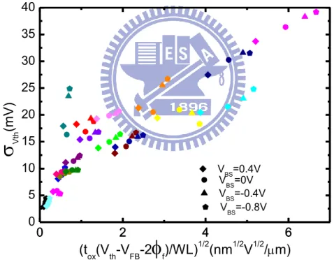
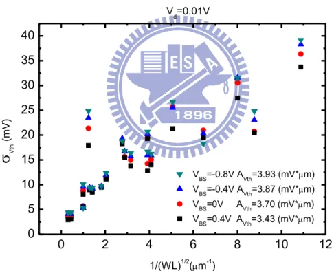
oxide thickness and threshold voltage, the results of this model are shown in Fig. 15.
From Fig. 15, we can observe obviously that the V standard deviation is being th
proportional to the inverse square root of the device area, and the mismatch became
severe with back-gate reverse bias. The result agrees well with the arguments as
mentioned above.
3.3 Random Dopant Induced Threshold Voltage Fluctuation
In above statements, we assume that impurity in the channel region has most
tremendous influence on threshold voltage fluctuation. As MOSFET scales down to
the deep submicrometer feature size, the intrinsic spreading in various parameters also
is a significant factor in the matching performance of the identically transistors. In
fact, the random dopant also plays an important role in the threshold voltage
fluctuation model.
In this work, we consider the effect of random dopant on the threshold voltage
fluctuation of the MOSFETs. The depletion region in the MOSFET increased while
the reverse substrate bias decreases in magnitude. Thus there exist extra dopants that
are now included in the depletion region and may induce the threshold voltage
fluctuation. This means that the mismatch in the body effect factor depends on
back-gate bias. But what we focus on is the threshold voltage fluctuation attributed to
a variation in the doping concentration, thus we can establish a threshold voltage
fluctuation model of channel doping to estimate the random dopant effect on the
In order to derive the channel doping fluctuation model, we start from Eq. (7),
and with Eq. (9) and Eq. (15), we can derive:
1/ 2 2 si(2 f BS) DEP A V W qN (18)
From Eq. (1), assuming the correlation coefficient of channel doping and other
parameters can be ignored, we can obtain:
2 2 2
, ,
th
V Vth dopant Vth others
(19) where Vth others, are the other unknown parameters that influence the threshold voltage fluctuation. We substituting Eq. (18) to Eq. (14) , we can derive a threshold
voltage fluctuation model of channel doping concentration [16]:
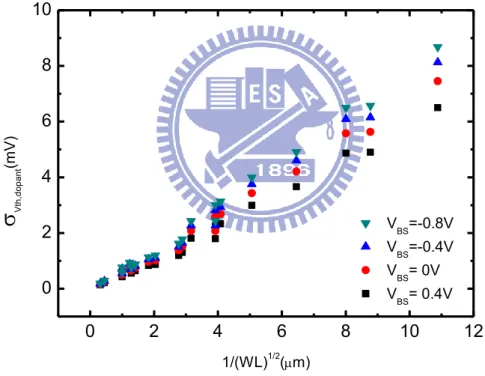
3 2 , 2 2 2 3 si f BS A Vth dopant ox q V N C WL (20)Here we still using the effective channel doping concentration extracted above. Fig.16
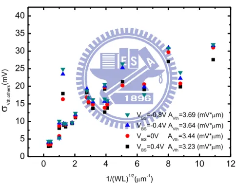
shows the results of calculated Vth dopant, by the model. By using Eq. (17), we can obtain the threshold voltage fluctuation effect due to the other unknown parameters as
shown in Fig. 17. Based on these results, we can observe that the channel doping
induced threshold voltage fluctuation is not obviously compared with other
parameters, especially for the large device. But from the threshold voltage fluctuation
model of channel doping concentration, we observe that when device size become
more and more small with the technology advancement, channel doping concentration
may become a more important factor of threshold voltage fluctuation.
In order to further discuss the effect of the random dopant, we take the boron
clustering effect into consider [17],[18]. In this case, the charge of carrier q is
replaced with nq and N is replaced with A NA/n . The threshold voltage is not
( )( / )
2 SUB DEP 2 SUB DEP
th FB f FB f ox ox nq N n W qN W V V V C C (21)
Then we can modify Eq. (20) into the form related with the number of boron atoms
per cluster:
3 2 , 2 2 2 3 si f BS A Vth dopant ox n q V N C WL (22)Fig. 18 shows the Vth dopant, of different number of boron atoms per cluster 1 ~ 6
n at zero back-gate bias. We can observe obviously that the boron clusters influences the Vth dopant, very significantly. When taking the boron clustering effect into consider, the random dopant effect on threshold voltage fluctuation become more
obviously. Fig.19 shows the Vth others, of different number of boron atoms per cluster 1 ~ 6
n . Therefore, the number of boron atoms per cluster must be taken into account while examining the threshold voltage fluctuation in the future.
Chapter 4
Mismatch Model Analysis and Modeling
4.1 Current Mismatch Model
It is widely known that the most important two parameters of mismatch are drain
current and threshold voltage. Here we will connect them and derive a mismatch
model in the following works. First, we define the current standard deviation as Id
and threshold voltage standard deviation as Vth. We use statistics tool to calculate the mean and standard deviation of our experiment data. In the subthreshold region,
the threshold voltage V affects the drain current th I through the following d
expression [5],[8]: th V q kT n d I Ae (23) Then we differentiate Eq. (23) and get:
th V q kT n d th q dI Ae dV kTn (24) The slope n can be written as:
' 1 1 ' 2 2 B ox f BS C n C V (25) 1/ 2 ' 2(2 ) si A B f BS qN C V (26)
and from Eq. (3), we can find S 2.3kT n q
,
where A is a constant, CB' is the junction capacitance per unit area , Cox' is the
oxide capacitance per unit area and S is the subthreshold swing. We choose
deviation is always the positive value, Eq. (24) can be applied with the absolute value
at both side. Since we can easily combine above-mentioned functions and build up a
mismatch model of current and threshold voltage [19]:
( / ) 0.06 ( / ) S V decade n V decade (27) d th I V d q I kT n (28) In previous works, we have extracted the subthreshold swing and standard
deviation of threshold voltage and drain current. Now we take them into this model,
assuming that the subthreshold swing mismatch is negligible here. The following are
the results of using our experiment to fit this model. Fig. 20 shows the result of our
experimental data at zero back-gate bias condition by using this model. From the
correlation, it can be found that the difference between the model and experimentally
extracted values are quite small.
4.2 Discussion of Current Mismatch Model
To make further use of this model, we observed that we can easily estimate the
standard deviation of threshold voltage with only the standard deviation of drain
current and subthreshold swing, and the result is worth being trusted. Eq. (28) can be
rewritten as follows: d th I V d nkT q I (29) Fig. 21 shows the comparison between the calculated result and the experiment, thus
confirming the validity of model. While this mismatch model has great estimation of
the fluctuation, there are two points that should be mentioned. First, this model is just
formula. Second, the applied current mismatch for different gate voltages might affect
the slope of the fit-line because the current mismatch changes with applied gate
voltage. Thus, besides the two points we mentioned-above, we can utilize this model
with ease.
We have extensively measured the n-type device over a small back-gate bias
range having different drawn gate widths and lengths. Experiment has exhibited that
the significant drain current mismatch occurs in weak inversion, especially for small
size devices. An analytic mismatch model has been developed and successfully
reproduced the extensively measured data. With the aid of this model, threshold
voltage mismatch can be expressed as a function of the process parameters, namely
the subthreshold swing and current variation. Examples have been given to
demonstrate that the model is capable of serving as a quantitative design tool for the
Chapter 5
Conclusion
At first, we have addressed the advantages and disadvantages of operating
MOSFETs in the subthreshold region, along with the discussions from different
aspects. Due to many related researches of mismatch, we have found that there are
two important characteristics of mismatch. One is process parameters that might
followed the inverse square root of the device area and the other is the back-gate
forward bias that might reduce the mismatch of the device.
Next, we have discussed the extraction of mismatch parameters. We have
obtained several important parameters including the threshold voltage, the
drain-induced barrier lowering, and the subthreshold swing. We have constructed a
new model to explain that the threshold voltage increases with the channel length
decrease and have confirmed it by experiment. After these parameters have been
extracted, we have further established the mismatch model. We have reproduced with
this model by the threshold voltage data and have made further discussions about the
influence of the random dopant and boron clusters. Finally, we have derived a useful
current mismatch model which can easily estimate the threshold voltage fluctuation
from the drain current mismatch in subthreshold region. The schematic flowchart to
summarize the procedure of our works is shown in Fig. 22.
Mismatch is indeed more and more important today, and our work is just a little
step in this direction. It is expected that our studies and the models might be helpful
References
[1] A. Pavasovic, “Subthreshold Region MOSFET Mismatch Analysis and Modeling for Analog VLSI Systems,” Ph. D. Dissertation, the Johns Hopkins University, 1991.
[2] E. A. Vittoz, “Micropower techniques”, in Design of MOS VLSI Circuits for Telecommunications, Y. Tsividis and P. Antognetti, Eds., Prentice-Hall, Inc., NJ. pp. 104-144, 1985.
[3] A. Papoulis, Probability, Random Variable and Stochastic Process, Kogakusha,
Tokyo:McGraw-Hill,1965.
[4] M. J. M. Pelgrom, A. C. J. Duinmaijer, and A. P. G. Welbers, “Matching properties of MOS transistors,” IEEE J. Solid-State Circuits, vol.24, pp. 1433-1440, October 1989.
[5] M. J. Chen, J. S. Ho, and T. H. Huang, “Dependence of Current Match on Back-gate Bias in Weakly Inverted MOS Transistors and It’s Modeling,” IEEE J.
Solid-State Circuits, vol. 31, pp. 259-262, 1996.
[6] A. Ortiz-Conde, F.J. García Sánchez, J.J Liou, A.Cerdeira, M. Estrada and Y. Yue, “A Review of Recent MOSFET Threshold Voltage Extraction Methods,”
Microelectronics Reliability, pp. 583-596, 2002.
[7] M. Tsuno, M. Suga, M. Tanaka, K. Shibahara, M. Miura-Mattausch and M. Hirose, “Physically-based Threshold Voltage Determination for MOSFET’s of All Gate Lengths. IEEE Trans. Electron Device, vol. 46, pp. 1429-1434, 1999.
[8] Betty Lise Anderson and Richard L. Anderson, Fundamentals of Semiconductor Devices, McGraw-Hill, New York, International edition, 2005.
[9] Asen Asenov and Subhash Saini, “Polysilicon Gate Enhancement of the Random Dopant Induced Threshold Voltage Fluctuations in Sub-100nm MOSFET’s with Ultrathin Gate Oxide,” IEEE Trans. Electron Device, vol. 47, pp. 805-812, 2000.
[10] Asen Asenov, “Random Dopant Induced Threshold Voltage Lowering and Fluctuations in Sub-0.1 m MOSFET’s: A 3-D “Atomistic” Simulation Study,” IEEE
Trans. Electron Device, vol. 45, pp. 2505-2513, 1998.
[11] Asen Asenov, “Intrinsic Parameter Fluctuations in Decananometer MOSFETs Introduced by Gate Line Edge Roughness,” IEEE Trans. Electron Device, vol. 50, pp. 1254-1260, 2003.
[12] Yiming Li, Shao-Ming Yu and Hung-Ming Chen, “Process-Variation-and Random-Dopants-Induced Threshold Voltage Fluctuations in Nanoscale CMOS and SOI devices,” Microelectronic Engineering, vol. 84, pp. 2117-2120, 2007.
[13] Yiming Li, Chih-Hong Hwang and Hui-Wen Cheng, "Process-Variation-and Random-Dopants-Induced Threshold Voltage Fluctuations in Nanoscale Planar MOSFET and Bulk FinFET Devices," Microelectronic Engineering, vol. 86, no. 3, pp. 277-282, 2009.
[14] K. Takeuchi, T. Tatsumi and A. Furukawa “Channel Engineering for The Reduction of Random-Dopant-Placement-Induced Threshold Voltage Fluctuation,”
IEDM 97, pp. 841-844, 1997.
[15] K. Takeuchi, T. Fukai, T. Tsunomura, A. T. Putra,A Nishida, S. Kamohara, and T. Hiramoto, “Understanding Random Threshold Voltage Fluctuation by Comparing Multiple Fabs and Technologies,” in IEDM Tech, pp. 467-470, 2007.
[16] Jeroen A. Croon, Maarten Rosmeulen, Stefaan Decoutere, Willy Sansen, and Herman E. Maes, “An Easy-to-Use Mismatch Model for the MOS Transistor,” IEEE
Journal of Solid-State Circuits, vol. 37, no. 8, pp.1056-1064, 2002.
[17] T. Tsunomura, A. Nishida, F. Yano, A. T. Putra, K. Takeuchi, S. Inaba, S. in Kamohara, K.Terada, T. Hiramoto, and T. Mogami, “Analysis of 5 Vth Fluctuation 65nm-MOSFETs Using Takeuchi Plot,” VLSI Symp. Tech. Dig., pp. 156-157, 2008.
[18] Takaaki Tsunomura, Akio Nishida, and Toshire Hiramoto, “Analysis of NMOS and PMOS Difference in VT Variation with Large-Scale DMA-TEG,” IEEE Trans.
[19] Pietro Andricciola and Hans P. Tuinhot, “The Temperature Dependence of Mismatch in Deep-Submicrometer Bulk MOSFETs,” IEEE Electron Device Letters, vol. 30, no.6, pp. 690-692, 2009.
0.0 0.2 0.4 0.6 0.8 1.0 1.2 10-9 10-8 10-7 10-6 VBS=0.4(V) VBS=0(V) VBS=-0.4(V) VBS=-0.8(V) I D (A) Vg(V) W=1m L=1m Vd=0.01V
Fig.1 The measurement ID mean and standard deviation in both subthreshold region
0.0 0.2 0.4 0.6 0.8 1.0 1.2 10-7 10-6 10-5 I D (A) VG(V) VBS= 0.4V VBS= 0V VBS=-0.4V VBS=-0.8V W=1m L=0.065m Vd=0.01V 0.0 0.2 0.4 0.6 0.8 1.0 1.2 10-7 10-6 10-5 I D (A) VG(V) VBS=0.4V VBS=0V VBS=-0.4V VBS=-0.8V W=0.6m L=0.065m Vd=0.01V
Fig. 2 The measured drain current versus gate voltage characteristics with different back-gate biases.
Fig. 3 Using constant current method to determine the threshold voltage in subthreshold region. 0.0 0.2 0.4 0.6 0.8 1.0 1.2 10-8 10-7 10-6 VBS=0(V) Vd=0.01(V) I D *(L m /W m )(A) VG(V)
The current we have chosen
Fig. 4 Measured mean threshold voltage with standard deviation versus the channel length for different back-gate biases.
0.0 0.2 0.4 0.6 0.8 1.0 0.00 0.05 0.10 0.15 0.20 0.25 0.30 0.35 0.40 0.45 W=10(m) Vd=0.01V Vth (V) L(m) VBS=-0.8V VBS=-0.4V VBS=0V VBS=0.4V 0.0 0.2 0.4 0.6 0.8 1.0 0.00 0.05 0.10 0.15 0.20 0.25 0.30 0.35 0.40 0.45 Vth (V) L(m) VBS=-0.8V VBS=-0.4V VBS=0V VBS=0.4V W=1(m) Vd=0.01V 0.0 0.2 0.4 0.6 0.8 1.0 0.00 0.05 0.10 0.15 0.20 0.25 0.30 0.35 0.40 0.45 W=0.6(m) Vd=0.01V Vth (V) L(m) VBS=-0.8V VBS=-0.4V VBS=0V VBS=0.4V 0.0 0.2 0.4 0.6 0.8 1.0 0.00 0.05 0.10 0.15 0.20 0.25 0.30 0.35 0.40 0.45 W=0.24(m) Vd=0.01V Vth (V) L(m) VBS=-0.8V VBS=-0.4V VBS=0V VBS=0.4V 0.0 0.2 0.4 0.6 0.8 1.0 0.00 0.05 0.10 0.15 0.20 0.25 0.30 0.35 0.40 0.45 W=0.13(m) Vd=0.01V Vth (V) L(m) VBS=-0.8V VBS=-0.4V VBS=0V VBS=0.4V
Fig. 5 The measured subthreshold swing versus gate length for different gate widths. 0.0 0.2 0.4 0.6 0.8 1.0 75 80 85 90 95 100 105 110 Su b th re sh o ld sw in g (mV/ d e ca d e ) L(m) W=10(m) W=1(m) W=0.6(m) W=0.24(m) W=0.13(m) Vd=0.01V VBS=0V
0.0 0.2 0.4 0.6 0.8 1.0 0.04 0.06 0.08 0.10 0.12 0.14 0.16 0.18 0.20 0.22 Me a n V th 1 (V) L(m) W=10m W=1m W=0.6m W=0.24m W=0.13m
Fig. 6 Measured mean threshold voltage versus L for different channel widths for Vd 1V.
0.0 0.2 0.4 0.6 0.8 1.0 0 50 100 150 200 250 300 Me a n D IBL (mV/ V) L(m) W=10m W=1m W=0.6m W=0.24m W=0.13m
0 2 4 6 8 10 12 0 5 10 15 20 25 30 35 40 D IBL st a n d a rd d e vi a io n (mV/ V) 1/(WL)1/2(m-1)
Fig. 8 The measured DIBL standard deviation versus the inverse square root of the device area.
Fig. 9 The measured and calculated V standard deviation versus the inverse th1
square root of the device area.
0 2 4 6 8 10 12 0 10 20 30 40 50 model exp
Vth 1 (mV) 1/(WL)1/2(m-1)
Fig. 11 The flat band voltage versus channel width at L=1m.
0.1 1 10 -0.7 -0.8 -0.9 -1.0 V FB (V) W(m) L=1m VBS=0V Vd=0.01V
NA_eff(cm-3) W=10 (m) W=1 (m) W=0.6 (m) W=0.24 (m) W=0.13 (m) L=1(m) 4.00E+17 4.00E+17 4.00E+17 4.00E+17 4.00E+17 L=0.5 (m)
5.92E+17 4.96E+17 5.04E+17 4.81E+17 5.05E+17
L=0.1 (m)
1.13E+18 1.16E+18 1.15E+18 1.12E+18 1.05E+18
L=0.065(m) 1.09E+18 1.16E+18 1.30E+18 1.44E+18 1.35E+18
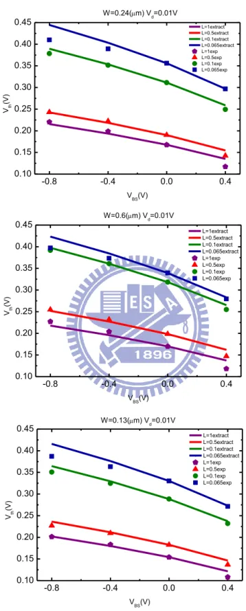
Fig. 13 Comparison of the Vth extracted from NA eff_ and the experimental data. -0.8 -0.4 0.0 0.4 0.10 0.15 0.20 0.25 0.30 0.35 0.40 0.45 W=0.6(m) Vd=0.01V Vth (V) VBS(V) L=1extract L=0.5extract L=0.1extract L=0.065extract L=1exp L=0.5exp L=0.1exp L=0.065exp -0.8 -0.4 0.0 0.4 0.10 0.15 0.20 0.25 0.30 0.35 0.40 0.45 W=0.24(m) Vd=0.01V Vth (V) VBS(V) L=1extract L=0.5extract L=0.1extract L=0.065extract L=1exp L=0.5exp L=0.1exp L=0.065exp -0.8 -0.4 0.0 0.4 0.10 0.15 0.20 0.25 0.30 0.35 0.40 0.45 W=0.13(m) Vd=0.01V Vth (V) VBS(V) L=1extract L=0.5extract L=0.1extract L=0.065extract L=1exp L=0.5exp L=0.1exp L=0.065exp
Fig. 14 Using measured data based on the fluctuation model to show the results of all device sizes for different back-gate biases.
VBS=-0.8V 0 2 4 6 VBS=-0.4V VBS=0V 0 2 4 6 0 5 10 15 20 25 30 35 40 VBS=0.4V
Vth (mV) (tox(Vth-VFB-2
f)/WL)1/2(nm1/2V1/2/m)0 2 4 6 8 10 12 0 5 10 15 20 25 30 35 40 VBS=-0.8V AVth=3.93 (mV*m) VBS=-0.4V AVth=3.87 (mV*m) VBS=0V AVth=3.70 (mV*m) VBS=0.4V AVth=3.43 (mV*m)
Vth (mV) 1/(WL)1/2(m-1) Vd=0.01VFig. 15 The measured standard deviation of threshold voltage difference versus the inverse square root of the device area for different back-gate biases.
0 2 4 6 8 10 12 0 2 4 6 8 10 VBS=-0.8V VBS=-0.4V VBS= 0V VBS= 0.4V
Vth ,d o p a n t (mV) 1/(WL)1/2(m)Fig. 16 The calculated Vth dopant, versus the inverse square root of the device
40 0 2 4 6 8 10 12 0 5 10 15 20 25 30 35 40 VBS=-0.8V AVth=3.69 (mV*m) VBS=-0.4V AVth=3.64 (mV*m) VBS=0V AVth=3.44 (mV*m) VBS=0.4V AVth=3.23 (mV*m)
Vth ,o th e rs (mV) 1/(WL)1/2(m-1)Fig. 17 The extracted Vth others, versus the inverse square root of the device area for different back-gate biases.
0 2 4 6 8 10 12 0.000 0.005 0.010 0.015 0.020 0.025 0.030 0.035 0.040 W10L1 W10L0.5 W10L0.1 W10L0.065 W1L1 W1L0.5 W1L0.1 W1L0.065 W0.6L1 W0.6L0.5 W0.6L0.1 W0.6L0.065 W0.24L1 W0.24L0.5 W0.24L0.1 W0.24L0.065 W0.13L1 W0.13L0.5 W0.13L0.1 W0.13L0.065 Vth ,o th e rs (V) VBS=0V 0.000 0.005 0.010 0.015 0.020 0.025 0.030 0.035 0.040 W10L1 W10L0.5 W10L0.1 W10L0.065 W1L1 W1L0.5 W1L0.1 W1L0.065 W0.6L1 W0.6L0.5 W0.6L0.1 W0.6L0.065 W0.24L1 W0.24L0.5 W0.24L0.1 W0.24L0.065 W0.13L1 W0.13L0.5 W0.13L0.1 W0.13L0.065 Vth ,o th e rs (V) VBS=-0.8V
0 2 4 6 8 10 12 0 5 10 15 20 n=6 n=5 n=4 n=3 n=2 n=1
Vth ,d o p a n t (mV) 1/(WL)1/2(m-1) VBS=0VFig. 18 The Vth dopant, with different number of boron atoms per cluster versus the inverse square root of the device area for zero back-gate bias.
Fig. 19 The Vth others, with different number of boron atoms per cluster versus the
inverse square root of the device area for zero back-gate bias.
0 2 4 6 8 10 12 0 5 10 15 20 25 30 35 40 n=1 n=2 n=3 n=4 n=5 n=6
Vth ,o th e rs (mV) 1/(WL)1/2(m-1)0.0 0.2 0.4 0.6 0.8 1.0 0 5 10 15 20 25
vth /n (mV)
ID/meanID
Id@Vgs-Vth~-0.1V VBS=0(V) Correlation:0.9409 Slope=25.43(mV)Fig. 20 The experimental data and fitting line from the drain current and threshold voltage mismatch model.
Fig. 21 The standard deviation of threshold voltage from model and experiment.
0 2 4 6 8 10 12 0 5 10 15 20 25 30 35 40