Physical and Electrical Characteristics of
Methylsilane-and Trimethylsilane-Doped Low Dielectric Constant Chemical
Vapor Deposited Oxides
Zhen-Cheng Wu,a, zZhi-Wen Shiung,a Chiu-Chih Chiang,aWei-Hao Wu,a Mao-Chieh Chen,a,
*
Shwang-Ming Jeng,bWeng Chang,bPei-Fen Chou,b Syun-Ming Jang,bChen-Hua Yu,band Mong-Song Liangba
Department of Electronics Engineering, National Chiao-Tung University, Hsinchu 300, Taiwan bTaiwan Semiconductor Manufacturing Company, Hsinchu, Taiwan
This work investigates the physical and electrical properties of two species of inorganic C-doped low dielectric constant共low-k兲 chemical vapor deposited共CVD兲 organosilicate glasses 共OSGs, ␣-SiCO:H兲. They are both deposited by plasma-enhanced CVD 共PECVD兲 processes using methylsilane 关共CH3兲SiH3, 1 MS兴- and trimethylsilane 关共CH3兲3SiH, 3 MS兴-based gases as the reagents, and are designated as OSG1 and OSG2, respectively. Experimental results indicate that the thermal stability temperature of OSG1 is 500°C, while that of OSG2 is 600°C, based on the results of thermal annealing for 30 min in an N2ambient. The deterioration of the low-k property in OSG1 is predominately due to the thermal decomposition at temperatures above 500°C of methyl (⫺CH3) groups, which are introduced to lower the density and polarizability of OSGs. For the Cu-gated oxide-sandwiched low-k dielectric metal-insulator-semiconductor共MIS兲 capacitors, Cu permeation was observed in both OSG1 and OSG2 after the MIS capacitors were bias-temperature stressed at 150°C with an effective applied field of 0.8 MV/cm. Moreover, Cu appeared to drift more readily in OSG1 than in OSG2, presumably because OSG1 has a more porous and less cross-linked structure than OSG2. The Cu penetration can be mitigated by a thin nitride dielectric barrier.
© 2001 The Electrochemical Society. 关DOI: 10.1149/1.1369373兴 All rights reserved. Manuscript submitted August 7, 2000; revised manuscript received January 3, 2001.
As the feature dimension of the device in integrated circuits共ICs兲 scales down below 0.18m, on-chip interconnects become a domi-nant factor in determining the overall IC chip performance, packing density, reliability, and manufacturing cost of deep submicrometer ultralarge-scale integrated共ULSI兲 circuits. With Cu successfully in-tegrated with SiO2using dual damascene processes in advanced sub-0.25m circuits for improved interconnect conductivity and reli-ability, the process integration of Cu with low dielectric constant 共low-k兲 dielectrics has also received extensive attention.1Realizing the robust combination of Cu and low-k dielectrics in the prevalent Cu dual damascene architecture will entail the further performance improvement in driving speed, crosstalk interference, and dynamic power dissipation by the reduction in the interconnect parasitic ca-pacitance共intra/interlevel capacitive load兲.2Currently, low-k dielec-trics are being extensively studied and developed on both organic 共carbon-based兲 and inorganic (SiO2-based兲 materials using both spin-on共SO兲 and chemical vapor deposition 共CVD兲 techniques.2-11 Low-k films deposited by CVD are lately attracting immense atten-tion for possible back-end-of-line 共BEOL兲 applications because CVD techniques provide several crucial advantages, such as supe-rior gap-filling capability and extremely uniform coating of large areas, which is necessary to future 300 mm wafers.12Furthermore, the CVD method is a dry process and generally needs fewer pro-cessing steps and lower propro-cessing costs than the spin-on method.3,5,12These characteristics make the CVD process easier for equipment manufacturers to integrate with other key processes, which may become a necessity for the final production yield con-sideration.
Among various low-k CVD films, SiO2-based dielectrics have attracted enormous interest because of their physical rigidity, me-chanical strength, and process extendibility, which together mini-mize integration risks and costs. Previous work has shown the ben-efits of incorporating fluorinated silicate glass共FSG, k ⫽ 3.5-3.7) into BEOL applications, as opposed to using the conventional un-doped silicate glass 共USG, k ⫽ 3.9-4.1).10,13,14 Nevertheless, ac-commodating dielectrics with even lower k values is inevitable as Cu interconnects are further scaled down to the 0.15/0.13m node.
C-doped low-k CVD organosilicate glasses共OSGs兲 become feasible candidates because of their lower k values共⬍3.0兲 than that of FSG. In this work, we investigate the thermal stability and electrical reli-ability issues of two species of newly developed OSGs, methylsilane- and trimethylsilane-doped oxides, with regard to inte-gration with Cu metallization.
Experimental
Electrical measurements were made on Cu- and TaN-gated oxide-sandwiched low-k dielectric metal-insulator-semiconductor 共MIS兲 capacitors. Figure 1 schematically illustrates the cross section of the Cu- and TaN-gated capacitors. The TaN-gated capacitors are used as control samples since TaN neither mixes with the silicon oxide layer nor oxidizes under the thermal conditions used in this study.15 Samples were prepared by first growing a 18 nm thick thermal oxide on p-type共100兲Si wafers at 1000°C in a dry oxygen atmosphere. This oxide layer is required to form a stable dielectric-to-substrate interface for well-behaved capacitance-voltage 共C-V兲 characteristics. Two species of low-k dielectric inorganic CVD or-ganosilicate glasses共OSGs, ␣-SiCO:H兲 were investigated; they are referred to hereinafter as OSG1 (k ⫽ 2.9-3.0) and OSG2 (k ⫽ 2.5-2.7), both of which were deposited over the thermal oxide to a thickness of 500 nm by plasma-enhanced CVD 共PECVD兲 pro-cesses in a parallel plate reactor operating at 13.56 MHz. The dis-charge was struck between two 26.3 cm diam electrodes spaced 300 mil apart. The OSG1 films were deposited using the gas mixture of methylsilane关共CH3兲SiH3兴 and nitrous oxide (N2O) as the reactive gases with the following conditions: substrate temperature, 17°C; total gas pressure, 1-10 Torr; rf power, 50-100 W; and (CH3兲SiH3/N2O flow ratio of 2/5. The OSG2 films were grown utilizing the gas mixture of trimethylsilane关共CH3兲3SiH兴 and oxygen (O2) as the reagents with the following conditions: substrate tem-perature, 350°C; total gas pressure, 1-10 Torr; rf power, 400-600 W; and (CH3兲3SiH/O2flow ratio of 1/6. A 50 nm thick PECVD USG
共undoped silicate glass, k ⫽ 4.2) was then deposited on the low-k CVD dielectrics. The USG films were deposited in a parallel plate reactor operating at 13.56 MHz at the following conditions: sub-strate temperature, 400°C; total gas pressure, 1-5 Torr; rf power, 1000-1500 W; and SiH4/N2/N2O flow ratio of 3/16/95. This oxide cap may be required to act as a chemical mechanical polishing 共CMP兲 hard mask in the Cu damascene architecture and a barrier to
*Electrochemical Society Active Member. zE-mail:[email protected]
Journal of The Electrochemical Society, 148共6兲 F127-F132 共2001兲 0013-4651/2001/148共6兲/F127/6/$7.00 © The Electrochemical Society, Inc.
minimize the absorption of moisture in the low-k films. Another split of samples with a 75 nm thick PECVD nitride 共SiN, k ⫽ 7-9) barrier replacing this oxide cap layer were also prepared to examine the SiN barrier effectiveness against Cu penetration. The SiN barrier was deposited in a parallel plate reactor operating at 13.56 MHz at the following conditions: substrate temperature, 400°C; total gas pressure, 1-5 Torr; rf power, 400-600 W; and SiH4/NH3flow ratio of 1/8. The samples underwent a degas bake at 400°C for 30 min in an N2ambient to remove absorbed moisture in the dielectric stack prior to the metal electrode deposition. A Cu film of 200 nm thickness was then sputter deposited using a dc magne-tron sputtering system with a base pressure of 1-2⫻ 10⫺6 Torr and no intentional substrate heating. The Cu surface was further covered with a 50 nm thick TaN overlayer, which was reactively sputtered in the same sputtering system without breaking the vacuum, using a Ta target in a gas mixture of Ar and N2with Ar/N2 flow rates of 24/6 sccm. The TaN overlayer prevents oxidation of the Cu layer in the subsequent high-temperature process. For the TaN-gated control samples, a 250 nm thick TaN layer was reac-tively sputter deposited directly on the oxide共USG兲 cap layer. A lift-off process, instead of a chemical wet etching of the vulnerable low-k dielectric stack, was used to define gate electrodes in a circu-lar area of 0.8 mm diam. A 1 m thick Al layer was thermally evaporated on the back side of the Si substrates for all samples to achieve a better contact for electrical measurements.
The completed Cu- and TaN-gated MIS capacitors were ther-mally annealed at 400°C for 1 h in an N2ambient. This annealing step eliminates the plasma damage during gate electrode sputtering, and provides the driving force for Cu permeation. The MIS capaci-tors were then bias-temperature stressed 共BTS兲 at 150°C with an effective applied field of 0.8 MV/cm for 30 min, which is long enough for the mobile charges to drift across the stacked insulator layer. The bias during BTS was provided by an HP 4145B semicon-ductor parameter analyzer, and the room temperature C-V charac-teristic was measured by a Keithley package 82 system. Notably, the MIS capacitors were first baked at 200°C on the thermal chuck for 1 h in the N2ambient to dehydrate the CVD dielectric stack prior to any BTS and/or electrical measurement and that all BTS measure-ments were performed with a continuous N2 purge to avoid the uptake of moisture in the CVD dielectric films throughout testing. High frequency C-V characteristics of the MIS capacitors, sweeping from inversion to accumulation, were measured at a frequency of 1 MHz.
Several techniques were utilized for intrinsic physical property measurements. Blanket samples of共OSG1, OSG2兲/thermal oxide/Si structures were prepared following the same processing sequence with the MIS capacitors used for electrical measurements except that both the upper USG cap layer and metal electrodes were omit-ted. Notably, the samples were first thermally annealed at 400°C for 30 min in an N2ambient to remove absorbed moisture in the CVD dielectric films prior to any physical analysis. The k value of the films was evaluated from the maximum capacitance values obtained from the high frequency C-V characteristics measured at 1 MHz on the Al-gated MIS capacitors; the area correction of the Al gate elec-trodes was made by optical microscopy共OM兲. Both the film thick-ness and the refractive index of the CVD dielectric layers were measured using a well-calibrated N&K analyzer at 6328 Å wave-length. Fourier transform infrared spectroscopy共FTIR兲 and thermal desorption mass spectroscopy共TDS兲 were used to characterize the chemical bonding evolution and outgassing behavior of the low-k dielectrics during the thermal annealing process. Rutherford back-scattering spectrometry 共RBS兲 was used to determine the atomic compositions of the OSG ␣-SiCO:H films. Secondary ion mass spectroscopy共SIMS兲 was employed to probe the possible presence of Cu in the dielectric stacks of the MIS capacitors.
Results and Discussion
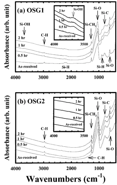
Physical properties and thermal stability of OSG1 and OSG2 dielectric films.—Figure 2 shows the thickness shrinkage and refrac-tive index for OSG1 and OSG2 thermally annealed at various tem-peratures. Evidently, the film thickness for OSG1 shrank 共⬎2%兲 upon annealing at temperatures above 500°C, and the refractive in-dex also exhibited a decreasing tendency, implying changes in film composition and bonding structure in OSG1, while similar changes to a minor extent were also observed for OSG2 at temperatures above 600°C. The reference value of 1.46 for the refractive index of the thermal oxides is indicated by a dashed line. Refractive indexes below 1.46 were proposed herein to indicate porous or less dense materials like OSGs.16In fact, these low density OSG films contain atomic scale nanoporosity or microvoid, which is closely related to the incorporation of CH3moieties into the films from organosilicon gas, (CH3)xSiH4⫺x.17-20 Figure 3 presents the FTIR spectra for OSG1 and OSG2 thermally annealed at various temperatures. Two remarkable features exist in the evolution of the absorption peaks. First, the Si-OH peak at about 3700 cm⫺1 did not appear in the Figure 1. Schematic cross section of Cu- and TaN-gated oxide-sandwiched
OSG1 and OSG2 MIS capacitors studied in this work. Figure 2. Temperature dependence of共a兲 and 共b兲 percentage shrinkage of film thickness and共c兲 and 共d兲 refractive index for OSG1 and OSG2 films.
FTIR spectra for either OSG1 or OSG2, indicating that the low-k CVD OSG dielectrics used herein were not susceptible to moisture uptake in the normal ambient. However, immersing the OSG1 film in boiling water for 30 min caused the Si-OH peak to appear in the FTIR spectra, whereas it remained stable for the OSG2 film even after immersion in boiling water for 2 h, as shown in Fig. 4. Despite the presumption that incorporating CH3groups into the Si-O net-work could cause OSGs to become hydrophobic, moisture uptake in OSG1 by immersing in boiling water may be associated with its porous structure.2-4,7,21 Since moisture uptake in the porous film should be easier because of the film’s effective larger surface area, OSG1 is presumed to be more porous than OSG2.22,23Such a sus-ceptibility to moisture may adversely affect the electrical reliability of OSG1 with respect to integration with Cu metallization. Second, both OSG1 and OSG2 are hybrid materials whose infrared spectra consist of both organic and inorganic absorption peaks. The organic Si-CH3 bonds reduce the density and polarizability of OSG films due to the steric hindrance of CH3groups, while the inorganic Si-O bonds constitute the main OSG network. The Si-O stretch peak at 1042 cm⫺1in OSG1 contains a shoulder at higher wavenumbers, indicating that the open chain and caged Si-O structural configura-tion coexist in this bond, whereas such a Si-O shoulder is unclear in OSG2. This major distinction of the Si-O bonding configuration implies different chemical bonding schemes between OSG1 and
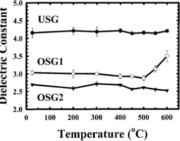
OSG2. Figure 5 shows the peak height ratio of Si-CH3共1273 cm⫺1兲 to Si-O 共1042 cm⫺1兲 in the OSG films. The peak height ratio in OSG1 remained constant at temperatures of up to 500°C, but dropped sharply at a temperature of 600°C共Fig. 5a兲, while the ratio in OSG2 remained unchanged all the way to temperatures of up to 600°C共Fig. 5b兲. Thus, degradation of the low-k property of OSG1, most importantly the k value, can be expected at temperatures above 500°C. Figure 6 shows the dielectric constants of OSG1 and OSG2 thermally annealed at various temperatures, with the data of USG included for comparison. The smaller k value of OSG2 than that of OSG1 represents a less polarizable bonding geometry in OSG2, de-spite the similar atomic ratio of C to Si共0.75-0.82兲, as determined by RBS, in both as-received OSG films studied herein. Moreover, as expected, the dielectric constant for OSG1 increased dramatically when temperatures exceeded 500°C. Conceivably, the k value in OSG1 deteriorated predominately because of the partial removal of the CH3groups, making the film prone to moisture uptake, and to appearing hydrophilic at localized areas on its surface. This result is further confirmed from the measured TDS spectra 共not shown兲, wherein the desorption of CH3increased markedly at temperatures above 500°C. In summary, the thermal stability of OSG1 was found to be 500°C, while that of OSG2 was 600°C, both higher than that of organic PAE-2 with aromatic structures.24
Figure 3. FTIR absorption spectra of 共a兲 OSG1 and 共b兲 OSG2 films
an-nealed at various temperatures for 30 min in an N2ambient.
Figure 4. FTIR absorption spectra of共a兲 OSG1 and 共b兲 OSG2 films
im-mersed in boiling water for various periods of time. The inset shows a part of the enlarged spectra.
Electrical characteristics of oxide-sandwiched OSG1 and OSG2 capacitors.—Figure 7 shows C-V curves of the Cu- as well as TaN-gated oxide-sandwiched OSG1 and OSG2 MIS capacitors before and after BTS at 150°C. The BTS was first applied with a positive bias共on the gate electrode兲 corresponding to an effective field of 0.8 MV/cm for 30 min, and followed by application with a negative bias under the same conditions. For both of the OSG1 and OSG2 capaci-tors, the negative flatband voltage shift (⌬VFB) of the Cu-gated capacitor resulting from the positive BTS was clearly larger than that of the TaN-gated capacitor, implying the presence of positively charged mobile Cu ions in both Cu-gated OSG1 and OSG2 films. Moreover, Cu ions obviously drift more readily in OSG1 than in OSG2. Such a fast permeation of Cu in OSG1 is presumably due to the more porous structure of OSG1, which contains high density nanometer-sized pores with radii of about 4-12 Å and total volume fraction of about 36%. These nanopores act as fast diffusion short-cuts via which Cu can drift rapidly in porous OSG1. Meanwhile, CVD dielectrics deposited at higher temperatures like OSG2 gener-ally possess a more cross-linked bonding structure that the Cu drift in OSG2 may be prohibited owing to the miniature free volume in the OSG2’s Si-O network.25-28Moreover, it was also reported that water vapor in the ambient greatly compounded the permeation of Cu in the oxide network, either by causing deep level electron traps,28,29or by hydration energy. As a result, even with continuous N2purging during BTS measurements, Cu drift in OSG1 may also be enhanced by the uptake of a trace of H2O, due to the suscepti-bility to moisture that differentiates OSG1 from OSG2. The smaller
negative⌬VFBassociated with the TaN-gated OSG1 capacitor com-pared with the Cu-gated counterpart resulted from the contaminated ionic charges, such as the alkali or hydrogen-related impurity in the upper USG cap layer.30This relationship can be verified by the fact that replacing the USG cap layer with a SiN cap layer resulted in negligible⌬VFB. These contaminated ionic charges may also exist in the USG cap layer of the OSG2 capacitor, but probably due to the sturdy cross-linked structure of OSG2, these ionic charges are not able to drift in OSG2 as easily as they did in OSG1. Meanwhile, the large positive⌬VFBand marked distortion in C-V resulting from the negative BTS on the Cu-gated and TaN-gated OSG1 capacitors may be associated with natural dielectric degradation, and is not related to Cu ion drift. These OSG1 capacitors were seriously damaged Figure 5. Temperature dependence of peak height ratios of Si-CH3/Si-O for
共a兲 OSG1 and 共b兲 OSG2 films, as determined from FTIR spectra.
Figure 6. Dielectric constant vs. annealing temperature for USG, OSG1, and
OSG2 films.
Figure 7. C-V characteristics of Cu- and TaN-gated oxide-sandwiched
OSG1 and OSG2 MIS capacitors before and after BTS at 150°C with an effective applied field of 0.8 MV/cm for 30 min. The positive共⫹兲 bias was applied first, followed by the negative共⫺兲 bias at the same conditions.
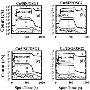
because a succeeding positive BTS induced many positive bulk charges and interface states. Such a dielectric degradation of OSG1 is presumably related to its intrinsic porous film structure that the OSG1 film is not able to withstand the stress field applied herein. Figures 8 and 9 show, respectively, the C-V curves and SIMS depth profiles of the BTS stressed Cu-gated OSG1 and OSG2 capacitors with a 75 nm thick SiN cap layer sandwiched between the OSG dielectrics and the Cu electrodes. The SIMS depth profiles of the Cu-gated USG capped OSG1 and OSG2 capacitors after the positive BTS are also included for comparison. The SiN cap layer achieves significant improvements in the OSG1 and OSG2 films, both in the absence of negative⌬VFBwith regard to the positive BTS, and in the absence of Cu penetration. Moreover, based on the results of SIMS depth profiles, the permeation of Cu appeared to be more severe in OSG1 than in OSG2. This finding was in complete accord with the results of electrical measurements that the negative⌬VFB resulting from the positive BTS on the Cu-gated OSG2 capacitors was much smaller than that on the Cu-gated OSG1 capacitors. Thus, it was concluded, from all the above observations, that the large
negative⌬VFBin the Cu-gated oxide-sandwiched OSG1 and OSG2 MIS capacitors was caused by the presence of Cu ions after the positive BTS, and the 75 nm thick SiN cap layer acted as an effec-tive dielectric barrier against Cu permeation.
Conclusion
Two species of inorganic low-k C-doped CVD organosilicate glasses共OSGs, ␣-SiCO:H兲 were assessed for their structural stabil-ity under various thermal annealing conditions and electrical reli-ability with regard to integration with Cu metallization. The thermal stability temperature of 1 MS-doped oxides共OSG1兲 was found to be 500°C, while that of 3 MS-doped oxides 共OSG2兲 was 600°C. Al-though Cu permeation was observed in both OSG dielectrics, Cu appeared to drift more readily in OSG1 than in OSG2. The distinct difference between the observed Cu drift behavior in OSG1 and OSG2 was presumably due to the more porous and less cross-linked structure of OSG1. Moreover, the nitride layer共75 nm兲 was verified to be an effective dielectric barrier against Cu penetration.
Acknowledgments
The authors thank Dr. Ming-Shih Tsai of NDL and Dr. Bing-Yue Tsui of NCTU for their valuable discussion and suggestions, and Chih-Jian Chen, Tien-I Bao, and Ai-Juan Chen of TSMC for their technical assistance.
National Chiao-Tung University assisted in meeting the publication costs of this article.
References
1. D. Edelstein, J. Heidenreich, R. Goldblatt, W. Cote, C. Uzoh, N. Lustig, P. Roper, T. McDevitt, W. Motsiff, A. Simon, J. Dukovic, R. Wachnik, H. Rathore, R. Schulz, L. Su, S. Luce, and J. Slattery, in Proceeding of 1997 IEEE IEDM, p. 773, IEEE共1997兲.
2. L. Peters, Semicond. Int., 1998, 64共Sept兲. 3. L. Peters, Semicond. Int., 2000, 52共Jan兲. 4. L. Peters, Semicond. Int., 1999, 56共Nov兲. 5. J. Baliga, Semicond. Int., 1998, 139共June兲.
6. M. Matsuura, Y. Hayashide, H. Kotani, T. Nishimura, H. Iuchi, C. D. Dobson, A. Kiermasz, K. Beekmann, and R. Wilby, in Proceedings of 1994 IEEE IEDM, p. 117, IEEE共1994兲.
7. M. Matsuura, I. Tottori, K. Goto, K. Maekawa, Y. Mashiko, and M. Hirayama, in Proceedings of 1997 IEEE IEDM, p. 785, IEEE共1997兲.
8. A. R. K. Ralston, J. F. Gaynor, A. Singh, L. V. Le, R. H. Havemann, M. A. Plano, T. J. Cleary, J. C. Wing, and J. Kelly, in Proceedings of 1997 IEEE VlSI Sympo-sium, p. 81, IEEE共1997兲.
9. M. Moussavi, G. Passemard, J. C. Maisonobe, and P. Turek, in Proceedings of 1999 IEEE IITC Symposium, p. 50,共1999兲.
10. W. Chang, S. M. Jang, C. H. Yu, S. C. Sun, and M. S. Liang, in Proceedings of 1999 IEEE IITC Symposium, p. 131, IEEE共1999兲.
11. M. Naik, S. Parikh, P. Li, J. Educato, D. Cheung, I. Hashim, P. Hey, S. Jenq, T. Pan, F. Redeker, V. Rana, B. Tang, and D. Yost, in Proceedings of 1999 IEEE IITC Symposium, p. 181, IEEE共1999兲.
12. T. M. Lu and J. A. Moore, MRS Bull., 1997, 28共Oct兲.
13. J. Ida, M. Yoshimaru, T. Usami, A. Ohtomo, K. Shimokawa, A. Kita, and M. Ino, in Proceedings of 1994 IEEE VLSI Symposium, p. 59, IEEE共1994兲.
14. T. Fukuda, T. Hosokawa, Y. Nakamura, K. Katoh, and N. Kobayashi, in Proceed-ings of 1996 IEEE VLSI Symposium, p. 114, IEEE共1996兲.
15. J. C. Chuang and M. C. Chen, J. Electrochem. Soc., 145, 4029共1998兲. 16. C. Falcony, J. C. Alonso, A. Ortiz, M. Garcia, E. P. Zironi, and J. Rickards, J. Vac.
Sci. Technol. A, 11, 2945共1993兲.
17. R. P. Mandal, D. Cheung, W. F. Yau, B. Cohen, S. Rengarajan, and E. Chou, in Proceedings of 1999 IEEE/SEMI Advanced Semiconductor Manufacturing Confer-ence, p. 299, IEEE共1999兲.
18. R. P. Mandal, V. Rana, M. Naik, D. Yost, D. Cheung, and W. F. Yau, in Proceed-ings of 1999 VMIC, p. 585共1999兲.
19. A. Grill and V. Patel, J. Appl. Phys., 85, 3314共1999兲.
20. B. K. Hwang, M. J. Loboda, G. A. Cerny, R. F. Schneider, J. A. Seifferly, and T. Washer, in Proceedings of 2000 IEEE IITC, p. 52, IEEE共2000兲.
21. A. Nara and H. Itoh, Jpn. J. Appl. Phys., 36, 1477共1997兲.
22. A. Jain, S. Rogojevic, S. V. Nitta, V. Pisupatti, W. N. Gill, P. C. Wayner Jr., and J. L. Plawsky, Mater. Res. Soc. Symp. Proc., 565, 29共1999兲.
23. N. Lifshitz and G. Smolinsky, J. Electrochem. Soc., 136, 2335共1989兲. 24. Z. C. Wu, C. C. Wang, R. G. Wu, Y. L. Liu, P. S. Chen, Z. M. Zhu, M. C. Chen,
J. F. Chen, C. I. Chang, and L. J. Chen, J. Electrochem. Soc., 146, 4290共1999兲. 25. A. L. S. Loke, J. T. Wetzel, P. H. Townsend, T. Tanabe, R. N. Vrtis, M. P.
Zussman, D. Kumar, C. Ryu, and S. S. Wong, IEEE Trans. Electron Devices, ED-46, 2178共1999兲.
26. Y. Uchida, K. Taguchi, T. Nagai, and M. Matsumura, in Proceedings of 1998 DUMIC, p. 46共1998兲.
Figure 8. C-V characteristics of Cu-gated and SiN-capped共a兲 OSG1 and 共b兲
OSG2 MIS capacitors before and after BTS. The conditions of BTS are the same as those of Fig. 7.
Figure 9. SIMS depth profiles of Cu-gated共a兲 capped OSG1, 共b兲
SiN-capped OSG2,共c兲 USG-capped OSG1, and 共d兲 USG-capped OSG2 MIS capacitors after a positive BTS at 150°C with an effective applied field of 0.8 MV/cm for 30 min. The Cu gate was removed prior to the SIMS measure-ments.
27. A. Grill, L. Perraud, V. Patel, C. Jahnes, and S. Cohen, Mater. Res. Soc. Symp. Proc., 565, 107共1999兲.
28. J. D. Mcbrayer, R. M. Swanson, and T. W. Sigmon, J. Electrochem. Soc., 133, 1242共1986兲.
29. Y. S. Diamand, A. Dedhia, D. Hoffstetter, and W. G. Oldham, J. Electrochem. Soc., 140, 2427共1993兲.
30. A. L. S. Loke, C. Ryu, C. P. Yue, J. S. H. Cho, and S. S. Wong, IEEE Electron Device Lett., EDL-17, 549共1996兲.