國 立 交 通 大 學
電子物理研究所
博士論文
全域組成氮化銦鎵薄膜之
磊晶成長與光學特性分析
Growths and Optical Properties of Entire
Composition of In
x
Ga
1-x
N Epilayers
研 究 生:陳京玉
指導教授:陳衛國 博士
全域組成氮化銦鎵薄膜之
磊晶成長與光學特性分析
Growths and Optical Properties of Entire
Composition of In
x
Ga
1-x
N Epilayers
研 究 生:陳京玉 Student:Ching Yu Chen
指導教授:陳衛國博士 Advisor:Prof. Wei-Kuo Chen
國 立 交 通 大 學
電子物理研究所
博 士 論 文
A Thesis Submitted to
Institute of Electrophysics
College of Science
National Chiao Tung University
in partial Fulfillment of the Requirements
for the Degree of
Doctor of Philosophy
in Electrophysics July 2010
Hsinchu, Taiwan, Republic of China
全域組成氮化銦鎵薄膜之
磊晶成長與光學特性分析
研究生:陳京玉
指導教授:陳衛國博士
國立交通大學電子物理研究所
摘要
在本論文中,我們利用在有機金屬化學氣相磊晶 (metalorganic chemical vapor deposition,MOCVD)系統上另行安裝一種氨預熱的裝置以增加熱分解效 率,藉由改變成長溫度與改變三甲基銦 (Trimethylindium,TMIn)之莫耳流量, 成功地成長全域組成氮化銦鎵(InxGa1-xN)薄膜。首先,薄膜成長溫度由 750 降低 至650 oC,固相銦組成可由 14 %增加至 40 %,由光激螢光光譜顯示,我們成功 地調變氮化銦鎵薄膜發光波長,並深入深紅光 738 奈米(nm)的波段,其譜線寬 度為180 meV。另外,當氣相比增加至 73 %時能將固相銦組成提高至 44 %,其 發光波長可進一步延伸至950 nm,譜線寬度為 235 meV。我們認為以另行安裝 一種五族預熱裝置以提高氨熱分解效率的方式,已能突破目前以 MOCVD 成長 氮化銦鎵薄膜無法達到全域組成皆能發光的瓶頸,特別是 650-1100 奈米波段, 遠超過目前商業MOCVD 的極限。 此外,透過光激發光光譜分析結果顯示,高溫成長的樣品(> 700 oC)會出現 高能量與低能量兩個發光譜峰,隨著成長溫度從 750-700 oC,高能量從 2.94 至2.58 eV,低能量從 2.44 至 2.07 eV,高低發光譜峰能量差約 500 meV。由倒置空 間圖譜(reciprocal space map,RSM)與陰極螢激發螢光譜(cathodoluminescence spectroscopy,CL)顯示高低發光譜峰分別來自薄膜下、上應力層(strained)與鬆弛
層(relaxed)所致。700oC 以下成長之樣品,由於銦組成較高與底層氮化鎵緩衝層
下,改變三甲基銦 (Trimethylindium,TMIn)之莫耳流量,探討固、氣相 In/III 族比值相互關係。實驗結果顯示,過高的氣相In/III 族比會產生大量金屬銦顆粒 析出於表面,直徑約3-5 微米不等,同時不利於高銦組成氮化銦鎵薄膜之成長。 此外,透過低溫14-K 光激發光光譜分析結果顯示,氮化銦鎵薄膜發光峰值可由 2.75 eV 至 1.29 eV,所涵蓋波長由藍光,綠光,紅光至近紅外波段。在這些樣品 中,發光之光子能量相對於吸收能隙其能量差(稱史塔克位移,Stokes shift),由 120 meV 增加至 570 meV 隨著銦組成的增加由 16 至 44 %,我們認為較大的史 塔克位移的現象歸因於銦含量分佈不均勻所造成。
Growths and Optical Properties of Entire
Composition of In
x
Ga
1-x
N Epilayers
Student:Ching-Yu Chen Advisors:Dr. Wei-Kuo Chen
Institute of Electrophysics
National Chiao Tung University
ABSTRACT
In this dissertation, the use of preheating ammonia installation can be used to increase the thermal decomposition efficiency of ammonia, we have demonstrated that the entire composition of InxGa1-xN epilayers prepared by MOCVD can be
achieved merely by varying the growth temperature and In vapor mole fraction. First, the In solid composition, as anticipated, was increased from 0.14 to 0.40 as the growth temperature decreased from 750 to 650 oC, which corresponds to a wavelength can be extends to the 738 nm in the deep red region with linewidth 180 meV. Further, as input In vapor mole fraction raise to 73 %, we could estimate that the In solid composition of the InxG1-xN films increases to 0.44, which corresponds to a
wavelength range extend to near infrared 950 nm with linewidth 235 meV. Therefore, we have surmounted the technique bottleneck of the absence of entire composition of InGaN epilayers, especially the emission wavelength 650-1100 nm.
For samples grown at temperature > 700 oC, separated by about 500 meV, two
emission peaks are observable. The corresponding emission peaks, namely high and low emission peaks, are shift from 2.94 to 2.58 eV and from 2.44 to 2.07 as the
from strained layer closer to GaN buffer and low energy from relaxed layer near the surface, as revealed by the results of high-resolution x-ray reciprocal space mapping (RSM) and cathodoluminescence (CL) measurements. For samples grown at temperature < 700 oC, high In content epilayers having a large lattice mismatch with under GaN buffer layer, the nearly absence of strained layer resulting in the feature of single emission peaks in both PL and CL spectra. In order to further extend the wavelength of the InGaN epilayer, we grew the InGaN sample at a growth temperature of 650 oC, in an attempt to investigate the dependence of InGaN solid composition on input In reactant flow rate. For the In solid composition, we thought that too high the TMIn flow rate will lead to decrease of In concentration solid, unfavorable to the high In content InGaN growth. Besides, we also reveals that the 14-K photoluminescence peak energy of InGaN epilayers exhibit a wide emission tunability from 2.75 to 1.29 eV, covering a wavelength ranges from blue, green, red and even reaches infrared 960 nm spectrum region. It shown that the bowing parameter of b ~ 2.3 eV for our results and the literature data for the band gap of InxGa1-xN over the entire composition. Our observation provides conclusive evidence
that the InxGa1-xN epilayers exhibits a larger Stokes shift, showing that the alloy’s
誌謝 (Acknowledgements)
終於走到寫誌謝的這一天了,回想起在交大的這幾年歲月裡,心中浮現的不 是畢業的喜悅,想到的也不是所做的實驗結果,感觸最深刻的是跟著我的大老闆 陳老師一起奮鬥的日子。WK2008 MOCVD 磊晶系統的架設是老師跟我們這一群 小伙子共同最深的回憶,從學弟阿德:學長完了我被老師秒殺,(結果每晚準備超 猛咖啡狂灌學長,還跑到台中學畫戰鬥機程式),最愛哭學弟毛頭:學長開甚麼玩 笑不可能做到的、學長我去廁所一下(偷哭),一直到第一片WK001 出產的那一 刻,透明的亮面的,來Mo 口號:不錯喔~ 到現在仍然環繞於耳,忽然間心裡不 禁會心一笑,這段讓我們充滿驕傲的回憶,大家一起打拼的日子,我們一輩子都 很難忘。 這段短短的致謝裡,我想我最要感謝的人就是我的恩師,我的大老闆陳衛國 老師,您無私的教導與鼓勵,所傳授給我最重要的經驗:「沒有做不到的事,只 有要不要做的心」,與從不放棄的「堅持」,真的讓我受益良多。畢業後我一定會 更加的努力,並且牢牢地記住老師曾經跟我說過的每一句話。一日為師,終身為 父,我們這群您帯出來的孩子絕對不會漏氣的,心裡的感謝實在無法用筆墨形 容,只有一句,感謝您所給與的一切。 另外,在這裡更要感謝周武清老師、張文豪老師與李明知老師在毎一次的會 議與研究上不厭其煩的叮嚀,您們的指導讓我對問題的思考有更深更廣的想法。 而我也要特別感謝已畢業的學長歐震、小柯、張富欽、李寧…等人,由於您們關 心與協助,才能讓我順利走完博士生涯。也要感謝中科院林文仁博士、程一誠博 士、林科均大哥、張大哥、李大哥、寬哥、家慶學長、阿瑞學長與皆智在我博士 班期間所給與的鼓勵與幫助。 而我也要特別感謝跟我一起努力的學弟妹們,少甫、芳葦、大尾、玨愷、勃 亨、國陞…等,在這段日子裡有你們真好,一定要好好加油,期待以後的相逢喔!還有,文哲你的妙傳讓我們打遍天下無敵手,林宣妳的網購有好康的(特別是龍 蝦沙拉)記得 call 我喔,阿賢、大雄,大家加油,能夠認識你們讓我在交大的生 活更豐富。 最後,我最要感謝我的爸爸媽媽,您們辛勞的工作,一路的支持與鼓勵,我 由衷的感謝您們無悔的付出,現在您的孩子終於有能力照顧您們了。還有我弟小 甫,也要感謝你在我努力的時候陪我一起吃消夜一起變胖。另外,在最後我要特 別特別感謝我的老婆辰嘉,在這段不算短的日子裡,謝謝妳辛苦的陪伴在我身 邊,妳的支持與付出一直是我最有力的後盾(所以工作後我會認命交出提款卡 的),也感謝妳這麼用心的照顧我們的亞亞寶貝,看著他一天天的長大你們真的 是我最大的財富。
Contents
Abstract (Chinese) I
Abstract (English) III
Acknowledgements V Contents VII
Lists of Table VIII
Lists of Figure IX
Chapter 1 Introduction 1
Chapter 2 Experimental Details 12
2.1 Metalorganic chemical vapor deposition system 12
2.2 Characterization Analysis 16
2.2.1 High Resolution X-Ray Diffraction System 16
2.2.2 Photoluminescence and Photoluminescence Excitation system 17
2.2.3 Atomic Force Microscopy 19
Chapter 3 Growth and Characterization of InN nanodots 28
3.1 Experimental detail of InN nanodots 29
3.2 Growth temperature effect of InN nanodots 32
3.3 Conclusions of InN nanodots growth 38
Chapter 4 Growth and Characterization of InxGa1-xN films Grown at
Various Temperatures
49
4.1 Experimental detail of InxGa1-xN films 51
4.2 Growth temperature effect of InxGa1-xN films 52
4.3 Conclusions of InxGa1-xN films growth 58
Chapter 5 In-rich InxGa1-xN films Growth 66
5.1 Experimental detail of In-rich InxGa1-xN films 68
5.2 Solid composition incorporation of In-rich InxGa1-xN films 69
5.3 Conclusions of In-rich InxGa1-xN films growth 75
List of Tables
Table 2-1 The source line details of MOCVD system for III-nitride growth 13
Table 3-1 The growth conditions of InN dots on GaN 31
Table 3-2 Average height, diameter, and electron concentration of the InN dot grown at temperature from 550 to 725 oC
33
List of Figures
Fig. 1-1 Historical and Predicted Efficacy of Light Sources 3
Fig. 1-2 (Top figure) A plot of the luminous efficacy for the human eye response as a function of wavelength. (Bottom figure) A plot of the spectral power distributions (SPDs) for three sources including: a fluorescent lamp, an incandescent lamp and a RYGB SSL white light source
5
Fig. 1-3 External quantum efficiency vs. peak wavelength for high-power LEDs based on InGaN LEDs and III-phosphide (InGaAlP light emitting layer) material systems
6
Fig. 2-1 The schematic diagram of piping equipment of MOCVD system 22
Fig. 2-2 The schematic diagram of reactor system 23
Fig. 2-3 Schematic diagram showing Bragg diffraction from planes of atoms in a crystal (b) shows part of (a) in detail
24 Fig. 2-4 Illustrates several basic types transitions in a semiconductor 25 Fig. 2-5 Photoluminescence and Photoluminescence excitation detection
system block diagram
26
Fig. 2-6 Schematic diagram of AFM system 27
Fig. 3-1 A chart showing the principle of the periodic flow rate modulation epitaxy growth InN dots on GaN buffer layer
42 Fig. 3-2 A time chart showing the modulation of reactant molar flow rate in
the periodic flow rate modulation epitaxy
43 Fig. 3-3 AFM images of InN dots grown at (a) 550, (b) 575, (c) 600, (d) 625,
(e) 650, (f) 675, (g) 700, and (h) 725 oC
44 Fig. 3-4 Arrhenius plots of InN dot density (solid circles) and growth
efficiency (open circles) as a function of growth temperature. The In droplet density (gray circles) is also shown in the figure
45
Fig. 3-5 Double-crystal XRD data (θ/2θ scan) of InN dots grown at various temperatures
46 Fig. 3-6 (a) 20-K PL spectra of InN nanodot samples grown by FME from 550
to 725 oC. The corresponding variations of peak energy and FWHM against growth temperature are shown in (b)
47
Fig. 4-1 Double-crystal XRD data (θ/2θ scan) of InGaN films grown from 650 to 725 oC, the inset shows the FWHM as function of In content (xsIn),
and (b) 14-K PL spectra of InGaN films. The corresponding variations of FWHM against xsIn are also shown in the inset figure
62
Fig. 4-2 XRD reciprocal space mapping of the (105) reflections of the 725
oC-sample (a) and 675 oC-sample (b), and the corresponding room
temperature CL spectra acquired at different electron beam energies are shown in (c) and (d)
63
Fig. 4-3 (a) 14-K absorption coefficient squared as a function photon energy. (b) 14-K PL peak energy and band edge determined by optical absorption as a function of xsIn. Some data are also shown (Ref. 20
and 21). The dashed curve shows the fit to the band gap energies (absorption) using a bowing parameter b=1.43 eV. The solid curve shows the fit to the band gap energies (PL) using a bowing parameter b=2.8 eV
64
Fig. 4-4 14-K Photoluminescence and photoluminescence excitation spectra of In0.38Ga0.62N films
65 Fig. 5-1 XRD θ-2θ curves of (0002) planes of InxGa1-xN films grown at
various TMIn flow rates. The inset shows the FWHM as functions of the In solid composition (xsIn)
79
Fig. 5-2 The surface morphologies of InGaN films grown at the TMIn flow rates of (a) 3.19, (b) 4.78, (c) 7.97, (d) 9.91, (e) 15.95, (f) 22.30 μmol/min, respectively
80
Fig. 5-3 (a) The In solid content (xsIn ) and growth rate, (b) the individual
growth efficiencies of GaN (γGaN) and InN (γInN) in ternary InxGa1-xN
as function of TMIn flow rate
81
Fig. 5-4 The 12-K PL sepatra of InxGa1-xN films as functions of the In solid
content (xsIn ). The corresponding variations of FWHM and intensity
against xsIn are shown insert figure
82
Fig. 5-5 14-K PL peak energy and band edge determined by optical absorption as a function of xsIn. Some data are also shown (Ref. 19 and 20). The
dashed curve shows the fit to the band gap energies (absorption) using a bowing parameter b=1.43 eV. The solid curve shows the fit to the band gap energies (PL) using a bowing parameter b=2.3 eV
Chapter 1 Introduction
In last decades, the wide-bandgap nitride semiconductors including indium nitride (InN), gallium nitride (GaN), aluminum nitride (AlN) and their alloys have played animportant role in optoelectronics devices. Due to their strong chemical bounds, high thermal conductivity and mechanical characteristic of III-V nitrides, they are superior materials for high temperature and high power devices [1-3]. Recently, InN band gap of 0.65 eV [4] has been reported by A. A. Klochikhin et. al., rather than 1.9 eV value accepted in the earlier days [5-7]. Therefore, their quaternary AlInGaN alloys exhibit a quite wide bandgap tunability from 0.65 eV for InN to 6.3 eV for AlN, covering a wavelength range from infrared, entire visible, to ultraviolet spectral regions. Among them, , the In-rich InGaN alloys are of potential importance for applications in many fields including high-brightness blue, green [8], and red light emitting diodes (LEDs) [9], full-spectrum multi-junction solar cells [10] and phosphor-free solid state lighting (SSL) [11].
Most of LED applications based on wide-bandgap InGaN semiconductors are related to single-color light applications, such as traffic signals, indicator light and signage display, the continual development of LEDs has advanced the technology to a stage beginning to replace the traditional light sources due to its longer lifetime, low consuming power and maintains cost. As far as the light illumination is concerned, the traditional light sources including incandescent, fluorescent (includes compact fluorescent and linear fluorescent) and high intensity discharge light sources have
dominated the last century of lighting. For incandescent light bulb, it consumes more than 95 % of the supplied energy as heat, leaving only a small fraction (~ 5 %) of the input energy converting into visible light. Consequently, the incandescent light bulb exhibits as quite low luminous efficacy, lying in the range from 3 to 20 lm/W [12]. Recent efforts have demonstrated that the luminous efficacy of incandescent source can be further advance to a value of 80 lm/W [13]. On the other hand, the fluorescent lamp, having the efficacy from 25 to 111 lm/W [12], is typically more efficient than incandescent lamp. Linear and compact fluorescent lamps through multi-photon phosphors can raise the efficacy to 200 lm/W [13]. Among all traditional light sources, high intensity discharge lamps (which include mercury vapor, high-pressure sodium lamps and metal halide) are currently the most efficacious commercial lamps, with efficacies range from 25 to 150 lm/W [12].
The history of LED development can be traced back to 1950s, in which the first semiconductor light emitting diode was demonstrated using gallium arsenide (GaAs) materials. In 1962, General Electric’s Advanced Semiconductor Laboratory invented the first visible spectrum LEDs. The red GaAsP-based LEDs, Green GaP-based LEDs were subsequently commercialized in the late of 1960s. However, the blue LEDs based on gallium nitride (GaN) material was not emerged in the market until 1990s, owing to the difficulties in preparing high-quality InGaN film. At present, the white light sources made from LEDs are primarily utilizing either blue or UV LEDs to stimulate fluorescent or phosphorescent to create white light, with efficacies superior to fluorescent and HID lighting sources [14].
Solid state lighting (SSL) is referred to lighting that uses semiconductor LEDs, organic light emitting diodes (OLEDs), or polymer light emitting diodes (PLEDs) as illumination sources. The SSL allow the energy directly convert into light via the manipulation of electrons in a solid, as opposed to incandescent bulbs use thermal radiation or fluorescent tubes. Figure 1-1 shows the historical and predicted efficacy for different light sources [15].
Although the efficiency of SSL based on LEDs is presently an emerging technology with potential to greatly exceed that of traditional light sources, and have already replaced traditional lamps in many applications, the greatest impact of SSL
will likely be in general illumination applications, which necessitate high energy conversion efficiency as well as high luminous efficiency of white light sources.
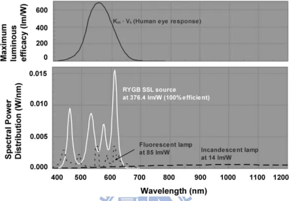
Fig. 1-2(a) shows a curve of the luminous efficacy of the human eye response. Fig 1-2(b) shows a plot of the spectral power distributions (SPDs) for three light sources including: a fluorescent lamp, an incandescent lamp and a RYGB SSL white light source. The human eye is sensitive to light with a wavelength between 400 to 700 nm, with a sensitivity peak at 555 nm. However, the radiation spectrum from the incandescent lamp is very broad, moreover, the filaments mitted in the infrared range, in such light bulbs convert more than 95 % of the supplied energy into heat, and with only a small fraction (~ 5 %) is converted to visible light. As shown at the bottom of Fig. 1-2, the spectrum of the fluorescent lamp is made up of blue, green and red illumination. Compare with incandescent lamp the fluorescent lamp achieved relatively high luminous efficacy. Nevertheless, the luminous efficacy of the 100 %-efficient four-color SSL (417 lm/W) is about 4 times greater than that of the fluorescent lamp and about 30 times greater than that of the incandescent lamp.
To achieve such SSL, significant challenges on LED technology must be overcome. One of the challenges for SSL is that high optical efficiency must be achieved across the visible spectrum to match the white light sources. When the light is generated from inorganic LEDs, much higher brightness than indicator optoelectronics devices is needed.
As shown in Fig. 1-3 the state-of-the-art external quantum efficiency (EQE) for LEDs measured at If = 350 mA is shown as a function of various wavelength [16].
The InGaN based high-power LEDs exhibit high EQEs in the wavelength between violet and blue regions, but rather poor EQE at longer wavelengths. At longer wavelength devices, achieved by increasing indium concentration in the InGaN active region, degraded InGaN material quality is resulted. This is attributed primarily to either the increased strain between GaN and InGaN layer or lower growth temperature associated with the MOCVD growth.
Fig. 1-2 (Top figure) A plot of the luminous efficacy for the human eye response as a function of wavelength. (Bottom figure) A plot of the spectral power distributions (SPDs) for three sources including: a fluorescent lamp, an incandescent lamp and a RYGB SSL white light source.
In regard with red LEDs, the current most efficient materials are (AlxGa1-x)yIn1-yP- based alloys.Its direct bandgap is available from x = 0 (InGaP), at ~
1.9 eV (~ 650 nm) to 0.53, at ~ 2.2 eV (~ 560 nm, green-yellow), beyond which the (AlxGa1-x)yIn1-yP becomes an indirect bandgap semiconductor, so that limiting
practical radiative wavelength to green-yellow ranges [17].
Although remarkable progress has been made in InGaN material growth, many efforts of InGaN study are focused on Ga-rich alloys, which are used as active layers in blue and green light emitting diodes. Relatively little attention has been paid to the
Fig. 1-3 External quantum efficiency vs. peak wavelength for high-power LEDs based on InGaN LEDs and III-phosphide (InGaAlP light emitting layer) material systems [16].
growth of In-rich InGaN alloys in spite of its potential importance in the fabrication of LEDs in the range from yellow to red wavelengths.
The difficulties in growing high In-content InGaN arise not only from the high vapor pressure of N2 over InN [18], high In desorption rate, but also from the low
solubility of InN in GaN solid miscibility gap, which usually results in the formation of phase separation in InGaN to deteriorate the film quality. I. The situation is getting even worse when MOCVD growth technique is employed for sample preparation since ammonia (NH3) is commonly used as N source precursor. Furthermore, in order
to reduce the volatility of indium, the growth temperature of In-rich InGaN epilayers is limited to the 550-650 oC. Unfortunately, this lower growth temperature results in poor crystalline quality due to the lower decomposition rate of NH3. In addition to the
effect of the lower growth temperature, we think that the low decomposition rate of NH3 resulting in the short supply of the active nitrogen atoms is one main reason
resulting in the poor quality of the MOCVD InGaN film grown at the low temperature. Although InGaN films seem to contain entire solid indium compositions, MOCVD-grown In-rich InGaN alloys still remains a matter of subject, especially for emission wavelengths in the range of 650-1100 nm, where no luminescent spectrum has yet been reported in the literature. In this dissertation, we will cover research in the fields of InN, Ga-rich and In-rich InGaN epilayers, and the incorporation behaviors of In on various MOCVD-growth parameters.
including MOCVD system and the characterization equipments, such as the x-ray diffraction, photoluminescence and atomic force microscopy measurement systems. The epitaxial growths of InGaN films as a function of growth temperature, together with the discussion of their optical propertied investigated by photoluminescence, x-ray reciprocal mapping, and absorption and photoluminescence excitation were described in chapter 4. In chapter 5, we discussed the incorporation behaviors of In on InGaN epilayers grown at 650 oC under various In flow rates. The anomalous temperature-dependent photoluminescence spectra were fitted well using thermal transfer model. Finally a general conclusion is presented in chapter 6.
Reference
[1] T. G. Zhu, D. J. H. Lambert, B. S. Shelton, M. N. Wong, U. Chowdhury, H. K. Kwon, and R. D. Dupuis: Electron Lett. 36, 1971 (2000)
[2] A. P. Zhang, J. Han, F. Ren, K. E. Waldrio, C. R. Abernathy, B. Luo, G. Dang, J. W. Johnson, K. P. Lee, and S. J. Pearton: Electronchem. Solid-State Lett. 4, G39 (2001)
[3] B. S. Shelton, D. J. H. Lambert, H. J. Jang, M. M. Wong, U. Chowdhury, Z. T. Gang, H. K. Kwon, Z. Liliental-Weber, M. Benarama, M. Feng, and R. D. Dupuis: IEEE Trans Electron Devices 48, 490 (2001)
[4] A. A. Klochikhin, V. Y. Davydov, V. V. Emtsev, A. V. Sakharov, V. A. Kapitonov, B. A. Andreev, H. Lu and W. J. Schaff: Phys. Rev. B 71 195207 (2005).
[5] K. Osamura, S. Naka, and Y. Murakami: J. Appl. Phys. 46, 3432 (1975).
[6] T. L. Tansley and C. P. Foley: J. Appl. Phys. 59, 3241 (1986).
[7] M. Yoshimoto, H. Yamamoto, W. Huang, H. Harima, J. Saraie, A. Chayahara, and Y. Horino: Appl. Phys. Lett. 83, 3480 (2003).
[8] D. Fuhrmann, C. Netzel, U. Rossow, A. Hangleiter, G. Ade, and P. Hinze: Appl. Phys. Lett. 80, 071105 (2006).
M. Watson, and K. P. O’Donnell: J. Phys. D: Appl. Phys. 35 604 (2002).
[10] J. Wu, W. Walukiewicz, K. M. Yu, W. Shan, J. W. Ager III, E. E. Haller, H. Lu, W. J. Schaff, W. K. Metzger, and S. Kurtz: J. Appl. Phys. 94, 6477 (2003).
[11] M. H. Crawford, Member, IEEE: IEEE J. Selec, Topic. In Quant. Electron. 15 1028 (2009).
[12] U.S. Department of Energy, Office of Energy Efficiency and Renewable Energy. Final Report: U.S. Lighting Market Characterization, Volume I: National Lighting Inventory and Energy Consumption Estimate. Washington, D.C. (2002).
[13] U.S. Department of Energy, Office of Energy Efficiency and Renewable Energy. Final Report: U.S. Lighting Market Characterization Volume II: Energy Efficient Lighting Technology Options. Washington, D.C. (2005)
[14] Efficacies of incandescent, fluorescent, and HID lamps from Audin, L., Houghton, D., et al. Lighting Technology Atlas. E Source, Inc., Boulder, CO: p 2.2.5 (1997)
[15] Luminous efficacies depicted are for:60 Watt incandescent lamp; 75 Watt halogen lamp; 100 -175 Watt HID lamp; 15 Watt CFL; and lumen equivalents of a 4-foot MBP 32Watt T8 lamp.
[16] D. Morita, M. Yamamoto, K. Akaishi, K. Matoba, K. Yasutomo, Y. Kasai, M. Sano, S. Nagahama, and T. Mukai: Jpn. J. Appl. Phys. 43, 5945 (2004).
[17] Th. Gessmann and E. F. Schubert: J. Appl. Phys. 95, 2203 (2004).
Chapter 2 – Experimental Details
This chapter briefly describes the experimental setup of deposition system and characterization tools such as x-ray diffraction, photoluminescence, and atomic force microscopy employed for studying material crystalline quality, surface morphology, and optical properties.
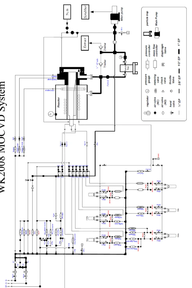
Owing to the different growth parameters required for depositions of InN and InGaN materials, two metalorganic chemical vapor deposition (MOCVD) systems were employed in this study. A home-made reactor system was utilized to grow InGaN epilayers, while a commercial system, Aixtron 200 RF-S horizontal reactor, was used to grow InN nano-dot samples.
2.1 Metalorganic chemical vapor deposition system
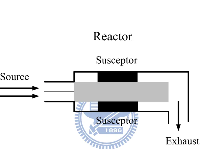
The home-built MOCVD system, equipped with a horizontal-reactor, mainly consists of six parts: a computer control system, a gas handling and gas-mixing system, a reactor chamber, a vacuum and exhaust system and the heating system. The corresponding schematic diagram of gas handling and gas-mixing system and the reactor design are shown in Fig. 2-1 and Fig. 2-2, respectively.
In this system, there are four metal-organic sources lines: trimethylgallium (TMGa), trimethylindium (TMIn), trimethylallium (TMAl) and bicyclopntadinarylmagnesium (CP2Mg) used for as the precursors of Ga, In, Al and
p-dopant, and three hydride lines, high-flow NH3, low-flow NH3 and SiH4, in order to
match the growth requirements needed in growing different In-content InGaN alloys. The MO sources are held in stainless steel bubblers immersed in thermostated baths with accurately controlled total vapor pressures to ensure steady supplies of all the source precursors. High-purity ammonia (NH3, 5N5, Air Porducts & Chem. Inc.) was
used as the N sources. The detailed parameters of source lines, such as, saturation vapor pressure, bubbler temperature, maximum flow rate of mass-flow controller are illustrated in Table 2-1. The switches and flow rate of each source precursor are controlled by main computer program via pneumatic valves and mass flow controllers (Bronkhorst-MFC) through PCI-1739U and PCI-1620A cards.
For MOCVD nitride growth, the susceptor, heated either by resistance heater or RF coil, provides not only a temperature needed for film deposition, but also the thermal energy to crack source precursors and generate reactive radicals to conduct chemical reaction on the growing surface. Since only a few percentage of NH3 can be decomposed at InGaN growth temperatures, approximately 600-800oC,in order to increase decomposition efficiency of NH3, many methods have been attempted,
including thermally pre-cracked ion-supplied method [1] and laser-assisted deposition[2-3].
For the former, the pre-heating device was commonly connected directly with NH3 gas tube right in front of reactor; nevertheless, even though the NH3 gases are
totally decomposed, the active nitrogen radicals still have to travel at least a distance of entrance length in the reactor before taking reactions with other reactants on the heated substrate surface. This weakens the activity of nitrogen radicals. Consequently, although the thermal precracking method can enhance the ammonia cracking to a certain extent, it does not bring a significant improvement of film quality for nitride deposition, in particular InGaN growth.
The special feature regarding our home-build MOCVD system is equipped with two heating units, as shown in Fig. 2-2. One is the lower graphite susceptor, on which the substrate is placed and thermally controlled at a growth temperature to perform the deposition of various epitaxial layers; the other is the upper graphite plate, disposed face-to-face to the lower one in the reactor, thermostated normally at a higher temperature for the purpose of pyrolyzing the hardly decomposed source
reactants, such as NH3.
Both heating plates are made of graphite, coated by high-purity silicon carbon (SiC) (POCO Inc.) to prevent or minimize any etching effects that could be brought about during the deposition. The upper graphite is inductively heated by a 30 kW, 30-80 kHz radio frequency (RF) generator; whereas the lower graphite is heated by a 50 kW, 30-100 kHz radio frequency (RF) generator. Both of graphite temperatures were monitored by R type thermocouples (Platinum/Rhodium alloy) surrounded by quartz sheaths, which were feedback controlled by Eurotherm 818P15 controllers.
High-purity hydrogen, generated by a palladium hydrogen purifier (Johnson Matthey HP-B-8549), was used as the main carrier gas. For InGaN deposition, nitrogen purified by a getter purifier (Japan Pionics Co., LTD) was instead used as carrier gas in order to suppress reevaporation of nitrogen atoms from the growing surface. Separated lines were designed in the gas-handling system so that the growth can be carried out in a complete H2 or N2 ambiant.
2.2 Characterization Analysis
2.2.1 High Resolution X-Ray Diffraction (HRXRD) System
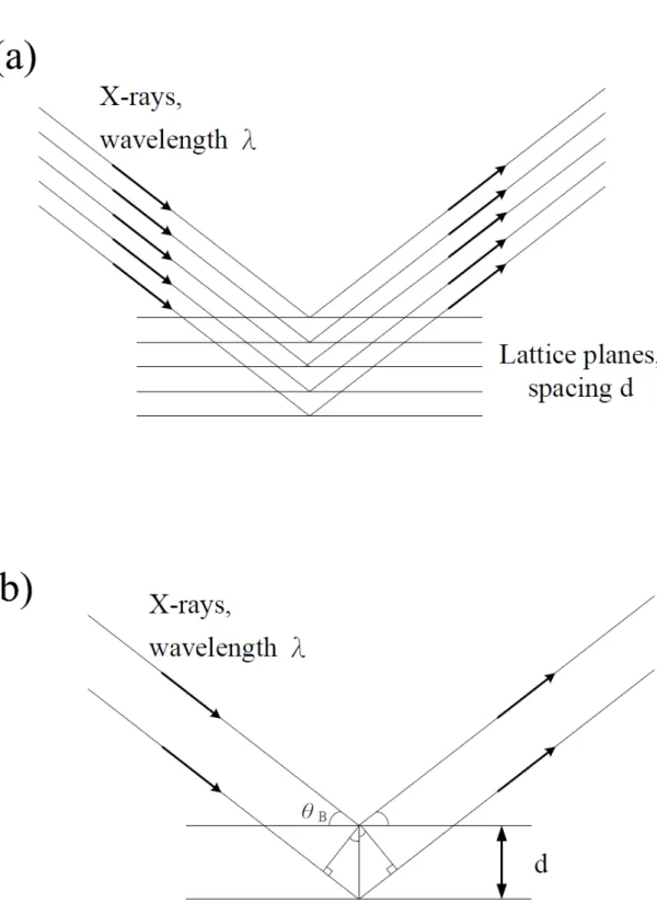
X-ray diffraction is a non-destructive method of analyzing the structural properties of a material. Double crystal x-ray diffraction is particularly adequate for the examination of materials with high crystalline quality, such as single crystal epitaxial films. Double crystal diffraction is high-resolution x-ray diffraction (HRXRD) technique, featured with a resolution as narrow as few arcseconds. Because of high-resolution capability, many fine multi-layered structures, even with layer thickness of 50 Å, can be analyzed with monolayer accuracy at interfaces. Furthermore, by taking experimental data into the simulation progarm, detailed information regarding the film structure, such as layer thickness and composition as well as degree of strain or relaxation can be well retrieved.
Since the wavelength of X-ray is comparable to the interatomic distances of crystal, when x-ray is incident into crystal, interference pattern is produced. Constructive interference occurs when the optical path of the x-ray scattered from neighboring planes of atoms is an integral number of wavelengths:nλ, where n is an integer. Under such a circumstance, i.e., Bragg diffraction condition, the diffracted intensity is maximum, as illustrated in Fig. 2-3 (a), (b). The equation is given below:
2dsinθ= nλ,
0.154051 nm (Cu Kα1), was used as the target of the x-ray source, d is the spacing of
adjacent parallel planes of atoms, θis the Bragg angle for diffraction, n is an integer, representing the order number of the diffraction.
2.2.2 Photoluminescence (PL) and Photoluminescence
Excitation (PLE) systems
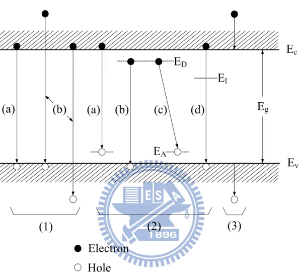
Photoluminescence spectroscopy is a fundamental tool to characterize the optical properties of materials, in which light is illuminated directly onto a sample, being absorbed to excite electrons from ground states to higher excited states. This process is called “photo-excitation”. When the excess energy is dissipated through the emission of light, such a luminescence process, is called photoluminescence. The intensity and spectral content of this photoluminescence is a direct measure of various material properties, such as GaN. In addition to radiative luminescence, there is alternative way to release the excess energy, which is referred to as nonradiative processes.
Fig. 2-4 illustrates several basic types of optical transitions in a semiconductor. [4] These transitions are classified as follows: The first one (1) is the interband transition, including (a) intrinsic emission correlated light emission with energy closed to bandgap, where excitons may play a dominant role under a low temperature environment, and (b) higher-energy emission involving energetic or hot carriers,
transition involving impurities or point defects; namely (a) conduction band to acceptor, (b) donor to valence band, (c) donor to acceptor (D-A pair emission), and (d) deep levels. The third classification (3) is the intraband transition involving hot carriers, also called deceleration emission. Not all transitions can occur during the photoluminescence measurement, and not all transitions are types of radiative processes. For an efficient luminescent material, its radiative transitions have to predominate over non-radiative ones (such as the Auger nonradiative recombination) [5].
In our laboratory, a He-Cd laser (Kimmon IK5552R-F) operating at 325 nm line (3.815 eV) was used as the excitation source for the photoluminescence measurement. The PL measurement system is shown in Fig. 2-5. The schematic diagram of PL and PLE detection systems includes the reflection mirrors, focusing and collecting lenses, sample holder and cooling system. The samples were mounted on the flat surface of copper holder cryostated at a temperature near 12 K. The typical excitation power density is of ~ 900 W/cm2, with a spot size of ~ 100 μm, as estimated from reflecting microscope objective with the magnification of 25. We used a single-grating monochromator (ARC Spectro Pro-500) equipped with an either photomultiplier tube (Hamamatsu R955 PMT) having high efficiency in the UV range or photon counter (Hamamatsu C1230) for PL detection. The normal applied voltage of PMT is 1000 V as determined from pulse height distribution (PHD) analysis. According to the reciprocal linear dispersion (1.67 nm/mm with 1200 grooves/mm grating), the entrance and exit slits are both opened to about 50 μm, the resolution is about 0.0835
nm at 325 nm. Moreover, because of the wide PL spectral range needed for III-nitride materials, an irradiance standard (Model 200C Optronic Laboratories) method was used to calibrate the overall spectral response (including collection lens, spectrometer and detector). The PL scan was performed by exposing the sample under excitation for about 0.1 to 10 second at a step of 0.1 to 1nm, and the data were transmitted through an 8255 I/O card and recorded by a computer.
The PLE detection system (PTI model 101) is very similar to that of PL detection system except the light source, where d a 150 W Xenon lamp (A-1010B arc lamp housing with LPS-220B lamp power supply) is used as a light source. The light is dispersed by a monochromator with SID-101 controller. The light entrance and exit slits were both opened to about 500 μm. The wavelength resolution is from 2 to 4 nm for PLE detection.
2.2.3 Atomic force microscopy (AFM)
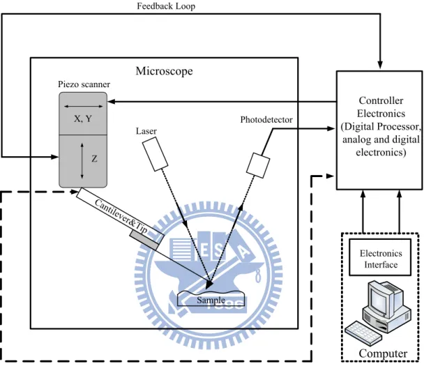
The atomic force microscope (AFM), invented by Gerd Binning and Calvin F. Quate consisted of a flexible, elastic cantilever and sharp probe tip, is a powerful tool that is capable of measuring interactive between atoms of the tip and sample surface by using scanning probe. Fig. 2-6 shows the configuration of AFM used in this study. The sharp tip is attached to a flexible cantilever, controlled by AC and DC voltages. When the AC signal was set at the resonance frequency, the cantilever will have
sample surface (X-Y plane) and (Z-axis), respectively. As the distance between the tip and sample surface is changed, the corresponding attractive and repulsive forces were also changed, which in turn bring a change of resonance amplitude and deflection of the cantilever. The degree of deflection is then sent to the control system and is used as the AFM signal. During the measurement, the microprobe is feedback controlled by a by piezo-electric crystal to bring the parameters back to its original values. From the deflection signals, we could analyze the sample surface morphology. There are three operation modes that can be used to scan surface morphology. In contact mode, the tip touches the surface while scanning over the sample. Although high resolution can be obtained in this way, the deformation of tips or samples often happens. Usually, non-contact is preferred to avoid the probe deformation since it utilizes the long rang Van der Waal’s force between the tip and sample. However, the sensibility and resolution is getting poorer because of the interference. For the surface potential microscopy it is necessary to use conductive cantilevers with a relatively small resonance frequency for operation in non-contact mode. An alternative is tapping mode. Tapping mode is a combination of contact mode and non-contact mode. Detection of tapping mode is more sensitive than that of non-contact mode and less destructive on probes than that in contact mode.
Reference
[1] A. Kim, K. Lee, H. Lee, K. Park, C. S. Kim, S. J. Son and K. W. Yi, J. Cryst. Growth 247 55 (2003).
[2] Y. Kangawa, N. Kawaguchi, Y. Kumagai and A. Koukitu, J. Cryst. Growth 272 444 (2004).
[3] A. G. Bhuiyan, T. Tanaka, K. Kasashima, A.Hashimoto and A. Yamamoto, Jpn. J. Appl. Phys 42 7284 (2003).
[4] H. F. Ivey, “Electroluminescence and Semiconductor Lasers, ” IEEE J. Quantum Electron., QE-2, 713 (1966).
Fig. 2-2
The schematic diagram of
Fig. 2-3 Schematic diagram showing Bragg diffraction from planes of atoms in a crystal (b) shows part of (a) in detail.
Fig. 2-4 illustrates several basic types transitions in a semiconductor
E
gE
cE
v(1)
(a)
(b)
(a)
E
DE
A(b)
(c)
E
l(d)
(2)
(3)
Electron
Hole
He-Cd Laser (λ=325 nm) Sample Cryogenic System ARC-Pro 500 Monochromator PMT
Photo Countor & Power Supply Mirror N. D. Filter Focusing Lens PTI Model 101 Monochromator
Xe compact arc lamp
Collecting Lens
Computer
Fig. 2-5 Photoluminescence and Photoluminescence excitation detection system block diagram.
Fig. 2-6 Schematic diagram of AFM system X, Y Z Piezo scanner Computer Electronics Interface Microscope Feedback Loop Laser Photodetector Cantilever &Tip Sample Controller Electronics (Digital Processor,
analog and digital electronics)
Chapter 3 - Growth and Characterization of InN nanodots
Recently, indium nitride has received considerable attention because of its superior intrinsic properties, such as narrow direct band gap, low effective mass, high electron mobility, and large drift velocity. [1-2] In addition, the use of InN and its alloys with GaN and AlN can extend its emission from the UV to the near-infrared wavelength, making it very suitable for the fabrication of light-emitting devices emitting at different wavelengths. Nevertheless, compared with other nitride semiconductors, InN binary epilayer remains one of the least studied materials owing to the low dissociation temperature, high saturation vapor pressure of nitrogen, and high In escaping rate associated with this type of material [3-4]. Even fewer efforts have been made on the study of its nano-scale physical structures. The first emission properties of InN dots were reported in 2005 in a study by Ruffenach et al. involving metalorganic vapor phase epitaxy (MOVPE), [5] in which the photoluminescence (PL) peak energy of InN dots encapsulated by SiO2 was found to be almost invariant to the measured temperature. The size tunable emission properties of InN dots, indicative of quantum size effect, have recently been realized by Ke et al. in 2006. [6] The associated peak energy was observed to blueshift systematically from 0.78 to 1.07 eV as the average dot height was tuned from 32.4 to 6.5 nm. On the other hand, the optical behaviors of InN nanodots directly exposed to air, i.e., without any capping layer, have not yet been reported. The uncapped surface quantum dots usually exihibit much weaker and broader PL properties than the capped ones, owing to the existence of a high density of trap states on the surface. In this work, we thus devote ourselves
to the study of uncapped InN nanodots by focusing on the dependence of their optical properties on growth temperature. Temperature dependent PL measurement reveals that good optical quality InN nanodots can be achieved in a wide growth temperature range, even at temperatures as high as 725 oC.
3.1 Experimental details of InN nanodots
In this study, the uncapped InN dot samples were grown on 1-um-thick GaN buffer layer/sapphire (0001) substrates by AIX 200 RF-S horizontal-reactor MOCVD system. The InN dots were deposited by flow-rate modulated epitaxy (FME) technique with six growth cycles at temperatures varied from 550 to 725 oC. The gas flow sequence for one growth cycle consists of four steps: 20 s trimethylindium(TMIn) step, 20 s NH3 step, intervened with a 10 s nitrogen carrier gas purge in between. The
TMIn and NH3 flow rates were 150 and 18000 sccm for the In and N steps, respectively. During the TMIn step, a small amount of NH3 at a flow rate of 500 sccm
was also provided to suppress the re-evaporation of In atoms in this step. The TMIn step is also referred to as the growth step because of the deterministic nature of group-III elements during deposition which governs the growth, whereas the NH3 step
is referred to as the annealing step, in which abundant NH3 is supplied to convert the
unreacted In atoms from the previous growth step into an InN form. The other detail grown conditions were described in Table 3-1. The PL measurements were performed using the 488 nm line of an argon-ion laser as an excitation source. The PL signals
analyzed by a 0.5m monochromator were detected by an InGaAs photodiode with a cutoff wavelength of 2.05 mm. The surface structures were examined by an NT-MDT atomic force microscopy (AFM) system, and images were taken using the noncontact tapping mode with a silicon cantilever.
The theory of the periodic FME growth according to this study is shown in Fig. 3-1. First, substrate 1 is provides (Fig. 3-1 (a)), and buffer layer 2 is grown on the substrate (Fig. 3-1 (b)). Purge gas 3 is turned on and the first reactant 4 is modulated to a range below the first molar flow rate (Fig. 3-1 (c)), so that the second reactant 5 turned on thereafter forms metal or metal-rich compound islands 6 on the buffer layer (Fig. 3-1 (d)). After the formation of said island, purge gas is turned on to clean remaining second reactant which does not form islands (Fig. 3-1 (e)). Subsequently, the first reactant 4 is modulated to a range above the second molar flow rate (Fig. 3-1 (f), so that said islands form high quality nanoparticles 7 with excellent structure under sufficient first reactant molar flow rate, and a growth cycle is completed. The geometric shape and size can be controlled through modulating the first and second reactant molar flow rates and the turn-on time.
The time chart of reactant precursor flow sequence is shown in Fig. 3-2. In the first purge step (as shown in Fig. 3-2 (a), purge gas (hydrogen 3) was turned on to clean remaining excess NH3 reactant, and NH3 reactant 4 was modulated to the lower
first molar flow rate range (2.23x10⁻² mole/min), so that TMIn reactant turned-on in next step was able to grow metal indium or In-rich islands on GaN buffer layer below the first molar flow rate without the formation of 2D grown InN film. Further, NH3
reactant was modulated to the lower first molar flow rate to avoid re-evaporation of nitrogen atoms on the surface of GaN buffer layer.
In TMIn reactant turn-on stage (as shown in Fig. 3-2 (b)), TMIn reactant 5 was turned on with molar flow rate setting of 1.20x10⁻⁵ mole/min for 20 seconds, to form metal indium of In-rich islands on GaN buffer layer. In the second purge stage (as shown in Fig. 3-2 (c)), TMIn reactant was turned off, and purge gas 3 was turned on for 5 seconds to clean remaining TMIn reactant which did not form metal indium or In-rich islands. In NH3 reactant turn-on stage (as shown in Fig. 3-2 (d)), the molar
flow rate of NH3 reactant 4, which was modulated from below the first molar flow
rate to above the second molar flow rate (8.04x10⁻¹ mole/min), was turned on for 10 seconds, so that islands formed InN nanoparticles 7 with excellent quality at sufficient
3.2 Growth temperature effect of InN nanodots
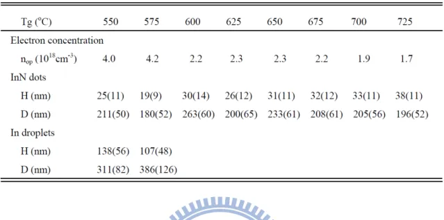
There is no doubt that growth temperature is one of the key parameters in determining the epitaxial properties of grown films and their nanostructures. We thus grew InN dots by FME at temperatures from 550 to 725 oC. The resulting AFM micrographs are shown in Fig. 3-3. As can be seen in the figure, truncated hexagonal InN nanodots, faceted by {10-12} or {10-13} planes, spread on the surfaces of all the samples. In droplets, formed either directly on the GaN surface or piled on the top surfaces of InN islands, occur only in samples grown at temperatures ≦575 oC. The corresponding structural properties, determined from AFM micrographs, and electron concentrations, estimated by analyzing the 20K PL spectra using a line-shaped model,[7] are summarized in Table 3-2. The average height for these InN dots ranges from 19 to 38 nm and their average diameter lies between 180 and 263 nm. Much larger heights were attained for metallic In droplets. Their heights and diameters are 138/311 and 107/386 nm/nm for samples grown at 550 and 575 oC, respectively. The variation in electron concentration seemingly coincides well with the aforementioned growth regions. Electron concentrations as high as (4.0-4.2)×1018 cm-3 are observed for those droplet-containing samples prepared at low temperatures. The electron concentration decreases to (2.2-2.3)×1018 cm-3 in the mid-temperature growth region and further decreases to ~1.7×1018 cm-3 when samples were prepared at 725 oC.
Fig. 3-4 shows an Arrhenius plot of InN dot density (solid circles) as a function of reciprocal temperature. For comparison, the In growth efficiency (open circles), defined as the ratio of growth rate to input In molar flow rate, is also included in the figure. Three distinct regimes can be clearly observed, namely, low-, mid-, and high-temperature grown regimes, separated by dividing temperatures of ~600 and 650
oC. It can be seen that the dot density increases markedly from 7×10⁷ to 8×108 cm-2 as
the growth temperature increases from 550 to 600 oC. It tends to increase slightly in the temperature range of 600-650 oC, starts to decrease rapidly at ~675 oC, and eventually disappears for temperatures >730 oC. The sharp decrease in dot density at high temperatures is considered to relate to the thermal etching or fast evaporation of adsorbed In atoms on the surface, as manifested by the observation of the onset of declining growth efficiency at these temperatures, also shown in Fig. 3-4.
Additionally, both the AFM micrpgraphs and X-ray diffractions indicate clearly that high densities 5-9×107 cm-2 of cone-shaped In droplets cover the entire surface for those low-temperature samples. (denoted by half-filled grey circles in Fig. 3-4) As shown in Fig. 3-5, signals of metallic indium (101) and (110) diffraction peaks (32.9 and 31.3o) are clearly observed in these low-temperature samples, in addition to those observed in the X-ray spectra of sapphire (006), 41.6o, GaN (001), 34.5o, and InN (002), 31.3o. The formation of droplets at low growth temperatures indicates an insufficient supply of active nitrogen radicals during deposition, stemming from the poor cracking efficiency of NH3 for temperatures <575 oC. Regarding the high-temperature growth regime ( > 650 oC), one might also expect the reappearance of In droplets on the surface as observed in conventional InN MOCVD growth, which has been proposed to be caused by the high desorption rate of N atoms from InN material itself at these temperatures. [8] However, this is not observed in our FME-grown InN samples. Neither In droplets nor their X-ray signals were detected. Our results suggest that the use of an FME scheme in InN dot growth, particularly the NH3 step, can suppress to a certain extent the decomposition of InN at high growth
temperatures and concurrently provide a way for unreacted In adatoms to change into the InN form.
The 20 K PL spectra for the above-described InN nanodots are shown in Fig. 3-6(a). The peak energies and full widths at half maximum (FWHMs) are shown in Fig. 3-6(b). Inferior optical properties were obtained for low-temperature-grown samples (550 and 575 oC), whose peak energies are located at approximately 0.80 eV
with FWHMs as high as ~100 meV. These emission energies are considerably higher than the reported band gap energy of 0.69 eV,[8] indicative of a strong Burstein-Moss effect due to the high electron concentration in these samples. Such a high electron concentration in these low-temperature-grown samples presumably originates from structural defects, such as stacking faults, voids, pits, or point defects, induced by the formation of In droplets on the surface, similar to the cases of GaAs and GaN systems.[9,10]
When the growth temperature is increased to 600 oC, these dots show marked improvement in their optical properties. Not only the peak energy and FWHM are improved to 0.77 eV and 71 meV, respectively, but also the PL intensity is markedly increased, almost by a tenfold increase in magnitude. The fairly good-optical-quality growth region remains not only in the temperatures of 600- 650 oC, but also, beyond our expectations, extends into the high-temperature region, where fast In desorption begins to occur. For those samples grown at temperatures > 650oC, the PL peak energy is shifted slightly toward a lower value, accompanied by a slow linewidth broadening in their PL spectra. Note that even for InN nanodots grown at 725 oC, the upper limit of our growth temperatures, reasonably good optical properties can still be obtained. The corresponding PL peak energy and FWHM are of 0.75 eV and 74 meV, respectively, comparable to typical results, 0.70-0.83 eV and 100-150 meV, for InN bulk films prepared by conventional MOVPE [11-13]. The results for these uncapped InN nanodots are quite encouraging. Although the linewidths (71-74 meV) are still large, they can already compete with those of the uncapped InAs and InGaAs surface
quantum dots (54-150 meV) [14-16]. In accord with study of InAs dots, the luminescent properties can be further improved significantly when dots are well capped by a suitable material, this sheds light onto future device applications of InN nanodots.
To gain more insight into the emission properties of these InN dot samples, we subsequently conducted temperature-dependent PL measurements. The results are plotted in Fig. 3-7 and compared with those for a 500-nm-thick InN bulk film grown at 625 oC. For the bulk film, the measured peak energy fits well with the Varshini-type band-gap shrinkage feature, E(T)=E0-αT2/(β+T) with =5.7110-4 eV/K, =900 K,
and a PL redshift of ~40 meV. With regard to InN nanodots, small blue shifts or slight shifts are observed for those low- and mid-temperature-grown samples. In contrast, clear redshifts of 15-20 meV are observed for samples grown at high temperatures. The corresponding Varshini’s parameters are in the ranges of (1.3-2.2) 10-4 eV/K and
400-500 K for and , respectively.
It has been calculated that the band-gap shrinkage for InN from 0 oC to room temperature due to the effects of lattice dilation and electron-phonon interaction is ~60 meV[17]. Thus, the large deviations of temperature-induced PL shifts from this value strongly suggest that there are blue-shift mechanisms to counterbalance the fundamental band-gap shrinkage in these InN nanodots. The corresponding displacements of peak energy in comparison with the band edge E0 are approximately
63-68, 60-62, and 40-45 meV for our low-, mid-, and high-temperature-grown InN dot samples, respectively. Such anomalous blue shifts were usually interpreted as the
successive filling of localized states [18] and/or band tail states [19] as well as the Coulomb screening of the piezoelectric electric field [20] by photogenerated or thermally released carriers.
The causes of the temperature-induced blue-shift mechanisms of InN nanodots studied here are still unclear at this stage. Aside from the combined effects of the above-mentioned mechanisms, we believe the surface electron accumulation may be the major cause responsible for the blue-shift in our nano-scale InN dots. This is described as follows. Owing to the high surface state density (~2.41013cm-2),Cimalla
et al. [21] reported that the free electron concentration for InN crystal thinner than 300 nm mainly comes from the surface electrons, rather than the bulk electrons. A recent study by Swartz et al [22] further pointed out that the surface electron concentration tends to increase significantly when the temperature is increased from 25 to 250K, whereas bulk electron concentration remains almost unchanged in this temperature range. Because the surface-area to volume ratio of dot is much higher than bulk material, much stronger surface electron accumulation is expected to be in InN dot structure. Consequently, as the measured temperature is increased, large amounts of trapped surface electrons of our InN nonodot samples are thermally agitated to the conduction band. This gives rise to an alleviated Fermi energy and hence an observed blue-shifted PL energy in the temperature-dependent PL spectra for these InN dot samples.
large densities of In vacancies arising from the fast evaporation of adsorbed In atoms during InN deposition. These In vacancies act as acceptors [23] in InN compensate the thermally stimulated surface electrons in this type of samples.
3.3 Conclusions of InN nanodots growth
We have investigated the PL properties of uncapped InN nanodots, prepared by flow-rate modulation epitaxy at growth temperatures from 550 to 725 oC. Our results indicate that the presence of In droplets on the surfaces of the low-temperature-grown samples indeed causes the deterioration of the optical properties. As for the high-temperature-grown samples (600-725 oC), where no droplets are formed, reasonably good luminescence results are attained. The corresponding PL peak energy shifts slowly from 0.77 to 0.75 eV with linewidth varying gradually from 71 to 74 meV as the growth temperature increases. Moreover, unlike the small blue shift or absence of variation in the samples grown at temperature < 650 oC, clear redshifts of 15-20 meV from 20 to 280 K were observed in our high-temperature InN dot samples, which are rarely seen in nanoscale InN structures.
Reference
[1]B. E. Foutz, S. K. O’Leary, M. S. Shur, and L. F. Eadtman: J. Appl. Phys. 85 (1999) 7727.
[2]A. G. Bhuiyan, A. Hashimoto, and A. Yamamoto: J. Appl. Phys. 94 (2003) 2779.
[3]H. Lu, W. J. Schaff, J. Hwang, H. Wu, W. Yeo, A. M. Pharkya, and L. F. Eastman: Appl. Phys. Lett 77 (2000) 2548.
[4]M. C. Lee, H. C. Lin, Y. C. Pan, C. K. Shu, J. Ou, W. H. Chen, and W. K. Chen, Appl. Phys. Lett: 73 (1998) 2606.
[5]S. Ruffenach, B. Maleyre, O. Briot, and B. Gil, Phys: Status Solidi C 2 (2005) 826.
[6]W. C. Ke, C. P. Fu, C. Y. Chen, L. Lee, C. S. Ku, W. C. Chou, W. H. Chang, M. C. Lee, W. K. Chen, W. J. Lin, and Y. C. Cheng, Appl. Phys. Lett: 88 (2006) 191913.
[7] B. Arnaudov, T. Paskova, P. P. Paskov, B. Magnusson, E. Valcheva, B. Monemar, H. Lu, W. J. Schaff, H. Amano, and I. Akasaki: Phys. Rev. B 69 (2004) 115216.
[8] A. G. Bhuiyan, A. Hashimoto, and A. Yamamoto: J. Appl. Phys. 94 (2003) 2779.
[9]I. Pietzonka, T. Sass, W. Seifert, S. Gray, and C. Mogensen: Jpn. J. Appl. Phys. 40 (2001) 6531.
Phys. Lett. 78 (2001) 3827.
[11] M. C. Johnson, S. L. Konsek, A. Zettl, and E. D. Bourret-Courchesne: J. Cryst. Growth 272 (2004) 400.
[12] A. Yamamoto, K. Sugitaa, H. Takatsuka, A. Hashimoto, and V. Y. Davydov: J. Cryst. Growth 261 (2004) 275.
[13] W. J. Wang, H. Miwa, A. Hashimoto, and A. Yamamoto: Phys. Status Solidi C 3 (2006) 1519.
[14] B. L. Liang, Z. M. Wang, Y. I. Mazur, G. J. Salamo, E. A. DeCuir, Jr., and M. O. Manasreh: Appl. Phys. Lett. 89 (2006) 043125.
[15] I. A. Karpovich, N. V. Baidus, B. N. Zvonkov, S. V. Morozov, D. O. Filatov, and A. V. Zdoroveishev: Nanotechnology 12 (2001) 425.
[16] Z. F. Wei, S. J. Xu, R. F. Duan, Q. Li, J. Wang, Y. P. Zeng, and H. C. Liu: J. Appl. Phys. 98 (2005) 84305.
[17] A. A. Klochikhin, V. Y. Davydov, V. V. Emtsev, A. V. Sakharov, V. A. Kapitonov, B. A. Andreev, H. Lu, and W. J. Schaff: Phys. Rev. B 71 (2005) 195207.
[18] P. G. Eliseev, P. Perlin, J. Lee, and M. Osinski: Appl. Phys. Lett. 71 (1997) 569.
[19] P. Perlin, V. Iota, B. A. Weinstein, P. Wisniewski, T. Suski, P. G. Eliseev, and M. Osinski: Appl. Phys. Lett. 70 (1997) 2993.
[20] H. Schömig, S. Halm, A. Forchel, G. Bacher, J. Off, and F. Scholz: Phys. Rev. Lett. 92 (2004) 106802.
[21] V. Cimalla, V. Lebedev, F. M. Morales, R. Goldhahn, and O. Ambacher: Appl. Phys. Lett. 89 (2006) 172109.
[22] C. H. Swartz, R. P. Tompkins, N. C. Giles, T. H. Myers, H. Lu, W. J. Schaff, and L. F. Eastman: J. Cryst. Growth 269 (2004) 29.
[23] C. Stampfl, C. G. Van de Walle, D. Vogel, P. Krüger, and J. Pollmann: Phys. Rev. B 61 (2000) R7846.
1 (a) 1 2 (b) 7 1 2 (f) 4 6 1 2 (d) 5 4 1 2 (c) 3 6 1 2 (e) 3 4 4
Fig. 3-1 A chart showing the principle of the periodic flow rate modulation epitaxy growth InN dots on GaN buffer layer.
Fig. 3-2 A time chart showing the modulation of reactant molar flow rate in the periodic flow rate modulation epitaxy.
Fig. 3-3 AFM images of InN dots grown at (a) 550, (b) 575, (c) 600, (d) 625, (e) 650, (f) 675, (g) 700, and (h) 725 oC.
0.95 1.00 1.05 1.10 1.15 1.20 1.25
10
810
910
10550
750 700
650
600
T (
0
C)
InN dot density
InN dot growth efficiency
In droplet density
Growth efficiency
(nm
3
/
mol)
Dot
/ droplet density (cm
-2
)
1000/T(K
-1
)
10
1210
1310
14Fig. 3-4 Arrhenius plots of InN dot density (solid circles) and growth efficiency (open circles) as a function of growth temperature. The In droplet density (gray cirles) is also shown in the figure.
30
32
34
36
38
40
42
44
7250C 7000C 6750C 6500C 6250C 6000C 5750C 5500C InN (002) In(101) GaN (001) In(110) Al2O3 (006)Inte
nsity
(a.u
.)
TH/2TH (degree)
Fig. 3-5 Double-crystal XRD data (θ/2θ scan) of InN dots grown at various temperatures.
Fig. 3-6 (a) 20-K PL spectra of InN nanodot samples grown by FME from 550 to 725 oC. The corresponding variations of peak energy and FWHM against growth temperature are shown in (b).
Fig. 3-7 Temperature dependences of the PL peak energies for our InN nanodot and bulk samples.
Chapter 4 - Growth and Characterization of InxGa1-xN films
Grown at Various Temperatures
The direct-bandgap InxGa1-xN alloys have been recently investigated intensively
because of the superior property of their wide spectral tuning capability, which can be changed continuously from ultraviolet to entire visible region and extended into near infrared region[1-3]. This offers many possibilities for this material in varieties of device applications, including high-brightness blue [4-6], green [7] and red light emitting diodes (LEDs) [8], full-spectrum multi-junction solar cells [9] and phosphor-free solid state lighting[10].
Despite of these peculiar features, up-to-date many efforts of InGaN study have been directed toward the Ga-rich alloys, which are used as active layers in blue and green light emitting diodes, few attempts have been made on In-rich InGaN (x>0.30). This is mainly due to the difficulties in obtaining high-quality InGaN films, attributed to the low solubility between InN and GaN, low dissociation temperature of InN as well as high equilibrium vapor pressure of nitrogen[11] associated with this material. The situation is getting even worse when metalorganic chemical vapor deposition (MOCVD) growth technique is employed for sample preparation since NH3 is
commonly used as N source precursor. Due to poor cracking efficiency, the pyrolysis of NH3 is necessitated to proceed at a higher temperature that imposes conflicting
temperature requirement of InN dissociation. Consequently, the MOCVD-grown InGaN film, particularly when the In concentration higher than ~25%, often
compositional fluctuation, In metal droplets and/or their complex point defects, which give rise to a drastic drop in luminescence efficiency. Even though the entire solid composition of InxGa1-xN epilayers without compositional inhomogeneity, as
examined by x-ray data, can be achieved by this method, the realization of high optical-quality, MOCVD-grown In-rich bulk InGaN alloys still remains a matter of subject, especially for emission wavelengths in the range of 635-1100 nm, where no photoluminescence data has yet been reported in the literature.
In this study, we have successfully grown InxGa1-xN epilayers with clear PL
signals by using MOCVD deposition method utilizing using by further investigate (with 0.18≦x≦0.4) grown at various temperatures by MOCVD. X-ray diffraction (XRD), photoluminescence (PL) measurements are employed to study the alloy compositions and PL emission bands of these InxGa1-xN films. Further,
photoluminescence excitation (PLE) measurements clearly indicates that the absorption from InGaN related band edge emissions even for higher In concentrations (>30%).
4.1 Experimental details of InxGa1-xN films
The In-rich InxGa1-xN epi-films employed here were grown on ~400 nm-thick
GaN/(0001) sapphire substrates using a home-made low pressure metalorganic chemical vapor deposition (MOCVD) system, equipped with a horizontal quartz reactor. Trimethylgallium (TMGa), trimethylindium (TMIn), and ammonia (NH3)
were used as Ga, In and N sources, respectively, and nitrogen was used as carrier gas. In order to enhance the decomposition efficiency, NH3 was thermally pyrolyzed
before conducting the chemical reactions with other reactants so that the growth can be performed at a lower temperature to minimize the effects caused by InN dissociation. The detailed description of NH3 pre-cracking method and reactor design
will be published elsewhere. During the deposition, the flow rates of TMGa, TMIn and NH3 were kept at 5.89, 8 mol/min and 4.8 L/min, repectively, while the growth
temperature was tentatively varied from 750 to 650 oC with the aim of obtaining different solid composition of epilayers. The resulted layer thickness was in the range of 400 nm. The as-grown epilayers were then examined by x-ray diffractometer (XRD) in θ-2θ scan mode of (002) reflection peak to estimate the In content in InxGa1-xN,
assuming Vegard’s law is valid.
PL measurements were carried out at T = 14 K using the 325-nm line of a He-Cd laser as an excitation source and a photomultiplier tube as a detector. Photoluminescence excitation (PLE) detection system (PTI model 101) is the same as the PL one except the excitation source that is provided by a 150W Xe lamp focused
4.2 Growth temperature effect of InxGa1-xN films
Fig. 4-1(a) shows XRD (002) θ-2θ patterns of the investigated InxGa1-xN films,
scanned from InN to GaN positions (31.3-34.5o). All samples appear to be single diffraction peaks. The lack of side diffraction peaks indicates no large variations in In contents or macroscopic phase separation in these samples. The measured In concentration, as anticipated, was increased from 0.14 to 0.40 as the growth temperature decreased from 750 to 650 oC, owing to the reduced In desorption rate at lower growth temperatures. The full widths at half maximum (FWHM) of x-ray curve is usually used as a figure of merit for crystalline quality. Normally a broader spectrum in the curve is resulted as the In content x closes to 0.5, because the synthesis of crystal has already enter the highly immiscible region in accord with the InGaN phase diagram predicted by thermodynamics, where separate crystals are easily formed to precipitate in the matrix. Nevertheless, we do observe a FWHM as narrow as ~700 arcsec for x=0.40 sample grow at 650 oC, which is compatible with that of low In-content InGaN films, suggesting the high crystalline quality of the layer.
Fig. 4-1(b) shows PL spectra of above InxGa1-xN films taken at 14K. For samples
grown at temperatures 700 oC, two emission peaks, separated by about 500 meV, are
observable. The corresponding emission peaks, namely high and low emission peaks, are shifted from 2.94 to 2.58 eV and from 2.44 to 2.07 eV as the In content is increased from 0.18 to 0.30. More delighted results were attained for those samples grown at lower temperatures, in which regardless a declining in PL intensity is
![Fig. 1-1 Historical and Predicted Efficacy of Light Sources [15]](https://thumb-ap.123doks.com/thumbv2/9libinfo/8215391.170257/15.892.124.710.486.907/fig-historical-predicted-efficacy-light-sources.webp)
![Fig. 1-3 External quantum efficiency vs. peak wavelength for high-power LEDs based on InGaN LEDs and III-phosphide (InGaAlP light emitting layer) material systems [16]](https://thumb-ap.123doks.com/thumbv2/9libinfo/8215391.170257/18.892.140.750.368.828/external-quantum-efficiency-wavelength-phosphide-ingaalp-emitting-material.webp)