國
立
交
通
大
學
資訊科學與工程研究所
碩
士
論
文
嵌 入 式 系 統 雙 指 令 J A V A 處 理 器 設 計
A Double-Issue JAVA Processor Design for Embedded Applications
研 究 生:柯厚任
指導教授:蔡淳仁 教授
嵌入式系統雙指令 JAVA 處理器設計
A Double-Issue JAVA Processor Design for Embedded Applications
研 究 生:柯厚任 Student:Hou-Jen Ko
指導教授:蔡淳仁 Advisor:Chun-Jen Tsai
國 立 交 通 大 學
資 訊 科 學 系
碩 士 論 文
A ThesisSubmitted to Institute of Computer Science and Engineering College of Computer Science
National Chiao Tung University in partial Fulfillment of the Requirements
for the Degree of Master
in
Computer Science
June 2007
Hsinchu, Taiwan, Republic of China
A Double-Issue JAVA Processor Design for Embedded
Applications
Abstract
Java applications for embedded systems are becoming popular today. CLDC/MIDP is the standard application platform for mobile phones while CDC/PBP is the emerging application platform for next generation digital TV set-top boxes. Although software-based Java Virtual Machines (VM) are prevalent, most of these VMs require a host processor running at much higher clock rate than 300MHz to reach reasonable performance. This is beyond the recommended specification of handsets and set-top boxes. In this thesis, we have proposed a double-issue java processor for embedded systems. The design is not tied to any host processors and can be used as an efficient binary execution engine for a full Java Runtime Environment implementation. When synthesized on a Virtex IV FPGA (4VFX12FF66-10), the RTL model can reach over 100MHz and consumes less than 23% resources of the device.
Acknowledgement
I would like to express my gratitude to all those who gave me the possibility to complete this thesis. First, I would especially like to thank my advisor, Professor Chun-Jen Tsai. He gives me a lot of motivation and suggestions. Also, he encourages me to think in various viewpoints to analyze the issue and create new ideas. Then, I appreciate the great help and comments from my seniors, juniors, and classmates. During these days at National Chiao-Tung University, I enjoy the moments studying with all MMES Lab members. Finally, I would like to thank my family for their supports and encouragement.
Content
I.
Introduction...10
II.
Previous Work ...13
1. Overview...13
2. Systems Using a Register File as a Stack Cache ...13
3. Systems Using On-chip Memory as a Stack Cache...16
4. Systems with a Two-level Stack Cache ...18
5. Other Designs...19
III.
Proposed Processor Micro-Architecture...22
1. Overview...22 2. Translation Stage...23 3. Fetch Stage...24 4. Decode Stage ...26 5. Execution Stage ...27 6. Memory Architecture ...28 7. Branch Behavior ...29
IV.
Peoposed Instruction Set Architecture...33
1. Overview...33
2. Data Path...35
3. Load Type Instruction ...37
4. Store Type Instruction ...39
5. ALU Type Instruction ...40
6. Nop or Special Type Instruction ...42
6.1. If_cmp<cond>...42
6.2. if<cond>...43
6.3. interrupt...44
6.4. Miscellaneous instructions of the special type...46
V.
Runtime Environment ...48
1. Overview...48
2. Simple Class Loader ...50
3.1. Global Format ...50
3.2. Constant Pool Info ...51
3.3. Field Info...53
3.4. Method Info ...53
4. Initialization of a Java Application for Execution ...54
VI.
Verification of the System...55
1. Synthesis and Co-design Tools ...55
1.1. Synplify Pro ...55
1.2. EDK – Embedded Development Kit...55
2. Emulation Platform: The Xilinx ML403 Board...57
3. The Test Program ...57
4. Experimental Results ...58
VII.
Discussions ...60
List of Figures
Fig.1. Sun’s picoJava...14
Fig.2. Generic Register File Approach...15
Fig.3. N:1 MUX Gate counts ...16
Fig.4. Using On-chip Memory as a Stack Cache ...17
Fig.5. A Two-level Stack Cache Approach ...18
Fig.6. A Two-level Stack Cache with Double Issue...20
Fig.7. Gate counts for a Two-level Stack Cache with Double Issue Architecture21 Fig.8. Overall Java Processor Architecture ...23
Fig.9. Translation Stage...24
Fig.10. Fetch Stage...26
Fig.11. Decode Stage ...27
Fig.12. Data Path of Execution Engine ...28
Fig.13. Memory Architecture ...29
Fig.14. Store branch triggered address...30
Fig.15. Fetch_one occur ...30
Fig.16. The decode stage start to decode the branch operation...31
Fig.17. The branch operation occurs...32
Fig.18. Encoding patterns of different types of instructions ...33
Fig.19. Instruction fields that signals operand count ...35
Fig.20. Data Path...36
Fig.21. Values of immROM ...37
Fig.22. Special type operations ...42
Fig.23. A standard Java Runtime System...49
Fig.24. Proposed Java Runtime System ...49
Fig.25. Runtime Class/Method Area ...50
Fig.26. Java Runtime Class Definition...51
Fig.27. Constant Pool Info ...51
Fig.28. Dynamic Resolution...52
Fig.29. Fast Resolution...53
Fig.30. Method Code Area ...54
Fig.31. Initialization of a Java Application ...54
Fig.32. Synplify Pro IDE...55
Fig.33. Embedded Development Kit...56
Fig.34. Overall Architecture...56
Fig.36. Compute Pi to 32 decimal points ...58 Fig.37. Experimental Result...59
List of Tables
Table 1. Gate counts for basic functions...15
Table 2. Gate counts for the Register File Approach...16
Table 3. Gate counts for a On-chip Memory Approach...18
Table 4. Gate count for Two-level Stack Cache Architecture...19
I. Introduction
Java Runtime Environment (JRE) is adopted by many organizations as the portable application platform for embedded systems such as mobile phones and set-top boxes. In order to support a large variety of devices while maintaining interoperability, Sun Microsystems has created the Java 2 Micro Edition (J2ME) specification and, under this framework, define different profiles and configurations for different applications [1]. For mobile phones, the Connected Limited Device Configuration (CLDC) with Mobile Information Device Profile (MIDP) has become the standard environment for Java applications. The virtual machine (VM) underneath CLDC/MIDP is a reduced-capability version of Java VM, called KVM. For DTV set-top boxes, the Connected Device Configuration (CDC) with Personal Basis Profile (PBP) are adopted as the de facto standard application environment [2]. The VM underneath CDC/PBP is a full capability VM. However, the reference implementation of CDC/PBP from Sun Microsystems is a specially engineered VM, called CVM, to facilitate porting to various embedded platforms.
There are many performance issues for adopting Java for embedded systems. First of all, object-oriented programs rely a lot on dynamic memory allocation/de-allocation which is very inefficient for embedded devices. Secondly, the Java VM model is based on a stack machine [3]. Excessive access of stack memory to store intermediate computation results is very inefficient. Finally, most embedded systems use a RISC CPU running at less than 300MHz as the host processor. The RISC architecture
is usually not efficient for the execution of a software interpreter of a byte-oriented machine language [4][5].
There have been many efforts to improve the performance of a Java VM [4]. For embedded devices, software-based approaches such as Just-in-Time[18][19] (JIT) compilation are less suitable since JIT compilers requires extra memory and the overhead of the on-the-fly compilation process is more noticeable and intrusive for embedded systems with slow RISC processors. In jHISC[13], the object-oriented related instructions are implemented by hardware directly, as a hardware-readable data structure is used to represent the object. For hardware-based solution, there are co-processor approaches (such as ARM Jazella[16]), hardware translation logic[14][17][20][21] and java processor approaches [5][6]. An interesting work is the Java processor, JOP, designed by Schoberl [5] since the complete RTL model (written in VHDL) is available to general public. JOP defines its own Java profile/configuration, which is closer to CLDC than a full JVM. The RTL model of JOP has been ported to many devices. However, the performance still has a lot of room for improvement. An enhancement of JOP is a real-time Java processor executed Java bytecode directly provides efficient support in hardware for mechanisms specified in the RTSJ (the real-time specification for Java) and offers a simpler programming model through ameliorating the scoped memory of the RTSJ. The most important characteristic of the processor is that its WCET (worst case execution time) of the bytecode execution is predictable. It is vital for the real-time systems.
The advantage of designing a stand-alone Java processor instead of a co-processor is that the design will not be tied to certain host processor interface. However, since a stack machine is not efficient for I/O and control tasks, a general purpose host processor is still required to complete the system. The key difference between the proposed Java processor and a Java co-processor is that it communicates with the host via a common memory-mapped interface, instead of a co-processor interface. The thesis is organized as follows. Chapter II discusses some related design of Java processors. The proposed double-issue Java processor architecture is presented in chapter III and the proposed instruction set architecture is presented in Chapter IV. Chapter V provides an overview to a full Java Runtime Environment design and discusses how a Java processor can be integrated into the environment. Finally, section VI describes the target FPGA platform and shows the synthesis report and experimental result of executing a Java class file using the synthesized model.
II. Previous Work
1.
Overview
In order to provide an efficient JRE for embedded applications, we have chosen the Java processor approach to improve the performance. There are many existing designs of Java processors. Since JVM is a stack-based machine, the main differences among these designs are about how the stack frames are implemented.
We classify the Java processors into three categories, that is, systems that include a register file as a stack cache, systems with on chip memory as a stack cache, and systems adopting a two-level stack cache. The system architecture for each design is described below. In order to make fair comparisons of their hardware costs, we assume that each system’s data cache has the same size.
2.
Systems Using a Register File as a Stack Cache
One of these designs is the picoJava [7] from Sun. There are many enhancements based on picoJava. In Radhakrishnan et al. [12], investigated ILP based on picoJava model. Sun’s picoJava contains 64 registers for stack cache which are organized as a circular buffer. This architecture is shown in Fig.1. It also contains a data cache with automatic spill and fill. Other design such as aJile’s JEMCore [8] contains 24 register entries. Only six of them cache the top elements of the stack. Ignite [9] processor has an operand stack which contains 18 registers entries.
1 2 3 4 5 6 7 8 9 10 11 12 13 14 15 16 17 18 19 20 21 22 23 24 25 26 27 28 29 30 31 32 33 34 35 36 37 38 39 40 41 42 43 44 45 46 47 48 49 50 51 52 53 54 55 56 5758 5960 61 62 63 64 Growing Shrinking Exec ution Uni t Da ta ca ch e Spill Fill
Fig.1. Sun’s picoJava
These designs have four pipelining stages.
IF : Instruction Fetch
ID : Instruction Decode
EX : Read Data from registers and Execute
WB : Write the result back to registers
With this architecture, the register file requires three read and two write ports. ALU operations can simultaneously read out two operands and write back one result. Concurrent background spill and fill operations keep the stack cache consistent with the top entries of the stack. The architecture for a generic register file approach is shown in Fig.2, and the rough gate count for each logic component is shown in Table 1.
Reg1
Reg2
………
RegN
Reg3
……
…
Data Cache
Result buffer
Fig.2. Generic Register File Approach Basic Function Gate counts
D-Flip-Flop 5
2:1 MUX 3
4:1 MUX 5
8:1 MUX 9
SRAM Bit 1.5
Table 1. Gate counts for basic functions
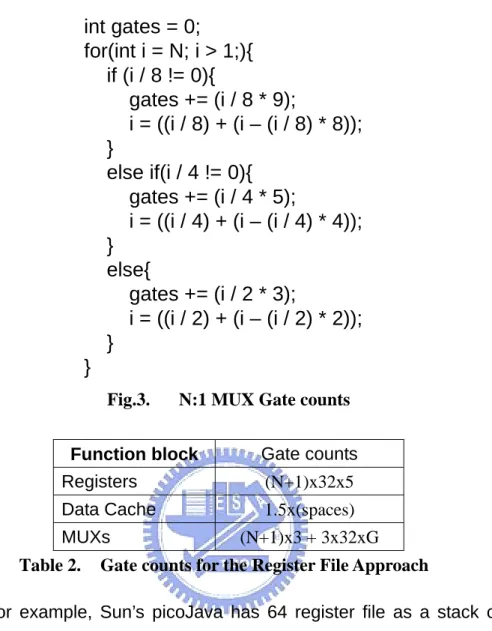
We assume that this processor contains N registers as a circular buffer. So it has N+1 2:1 MUXs and 3x32 N:1 MUXs. The formula calculating gate counts of N:1 MUX is shown in Fig.3. Let the gate count for an N:1 MUX be G. The gate counts of all the MUXs are (N+1)x3 + 3x32xG. The other sequential logics such as the registers and the data cache are composed of (N+1)x32x5 and 1.5x(number of bits) gates, respectively. The approximated result is listed in Table 2.
int gates = 0;
for(int i = N; i > 1;){
if (i / 8 != 0){
gates += (i / 8 * 9);
i = ((i / 8) + (i – (i / 8) * 8));
}
else if(i / 4 != 0){
gates += (i / 4 * 5);
i = ((i / 4) + (i – (i / 4) * 4));
}
else{
gates += (i / 2 * 3);
i = ((i / 2) + (i – (i / 2) * 2));
}
}
Fig.3. N:1 MUX Gate counts
Function block Gate counts Registers (N+1)x32x5 Data Cache 1.5x(spaces) MUXs (N+1)x3 + 3x32xG
Table 2. Gate counts for the Register File Approach
For example, Sun’s picoJava has 64 register file as a stack cache. Assume that it uses a 128x32 bits data cache, the approximated gate counts exclude ALU is 24515.
In JEMCore [8], only six registers are used to cache the top elements of the stack. This design decreases gate counts to about 11915 gates (assume that the data cache space is the same). Ignite [9] has 18 register file as a stack cache and costs about 11449 gates.
3.
Systems Using On-chip Memory as a Stack Cache
Komodo [10] and FemtoJava [11] use an on-chip memory as a large stack cache. You can see in Fig.4 that a three-port memory is required to
support the operation. There are five pipelining stages in their design:
IF : Instruction Fetch
ID : Instruction Decode
RD : Memory Read
EX : Read Data from registers and Execute
WB : Write the result back to registers
Stack RAM Result buffer Read Addr 1 Read Addr 2 Write Addr Write data Forward buffer
Fig.4. Using On-chip Memory as a Stack Cache
We can calculate gate counts in the same way as in the previous section. The simplified gate count for basic function is shown in Table 1. It has 3x32 2:1 MUXs and 32x4 registers. The approximated result is shown in Table 3. We assume that it uses 128x32-bit data cache. Its gate counts exclude ALU is about 7072. This approach is much smaller than previous approach. However, it uses three-port memory for the design and the hardware cost is much higher than the other approach. Although it can use
two dual-ports RAM to emulate three-port memory, this solution still double the amount of memory required.
Function block Gate counts
Registers 640
Data Cache 1.5x(spaces)
MUXs 288
Table 3. Gate counts for a On-chip Memory Approach
4.
Systems with a Two-level Stack Cache
Schoberl [5] presented the Java Optimized Processor (JOP) adopting a two-level stack cache. It uses two registers to store the top two elements of the stack, and a dual-port RAM to store the rest of the stack elements. It has three pipelining stages:
IF : Instruction Fetch
ID : Instruction Decode
EX : Read Data from registers and Execute
The architecture of JOP is depicted in Fig.5.
Stack RAM Read Addr Write Addr Write data A B
The gate counts of JOP can be estimated as follows. Roughly speaking, the architecture can be implemented using 2x32 registers, 3x32 2:1 MUXs, 128x32 bits data cache, and an ALU. The gate count approximations for each type of logic are shown in 0. The total gate count excluding ALU is 6752. This approach is much smaller than the register file approach and uses only one dual-port RAM for the design. It is more suitable for embedded systems.
Function block Gate counts
Registers 320 Data Cache 1.5x(number of bits)
MUXs 288
Table 4. Gate count for Two-level Stack Cache Architecture
5.
Other Designs
LavaCORE [22] uses a 32x32-bit dual-ported RAM to implement a register-file. The Lightfoot [23] 32-bit core is a hybrid 8/32-bit processor based on the Harvard architecture. Moon’s [24] stack folding is implemented in order to reduce five memory cycles to three for instruction sequences like push-push-add. Cjip [25][26] is a 16-bit CISC architecture with on-chip 36KB ROM and 18KB RAM for fixed and loadable microcode. Most of these designs are too complex for embedded systems.
In this thesis, we propose a two-level stack cache with double-issue architecture for Java processor. We use three registers to store three top of the stack elements. “A” is top of the stack, “B” is the 2nd top of the stack, and “C” is the third stack element from the top. The other stack elements are stored in two dual-port RAMs. There are four pipelining stages in our design.
TR : Bytecode fetch and translate on-the-fly
IF : Instruction Fetch
ID : Instruction Decode
EX : Read Data from registers and Execute
Stack RAM Read Addr1 Write Addr1 Write data1 A Stack RAM Read Addr2 Write Addr2 Write data2 B C
Fig.6. A Two-level Stack Cache with Double Issue
The design contains 10x32 2:1 MUXs, one 4:1 MUX, and 3x32 registers. The approximated gate count is shown in 1. We also assume that it uses 128x32-bit data cache. The total gate count excluding ALU is 7584. The gate count of this design is a little more than the two-level stack cache design used in JOP. However, JOP uses single issue architecture while the proposed design adopts double-issue architecture. Therefore, the computation ability is much higher than that of JOP.
Function block Gate counts
Registers 480 Data Cache 1.5x (number of bits)
MUXs 965
Fig.7. Gate counts for a Two-level Stack Cache with Double Issue Architecture
III. Proposed Processor Micro-Architecture
1.
Overview
In this section, the detail design of a double-issue Java Processor is presented. For a double-issue processor, two machine instructions are executed per cycle. It is important to point out that a Java processor in general does not execute bytecodes directly because some bytecodes are much more complex than a traditional machine instruction. Therefore, for the proposed processor, the native instruction set (referred to as the microcodes, following the convention in [5]) is different from the bytecode instruction set. A bytecode will be translated into one or more microcodes on-the-fly. The proposed processor has a four-stage pipeline which is shown in Fig.8. We have four pipelining stages :
TR : Bytecode fetch and translate on-the-fly
IF : Instruction Fetch
ID : Instruction Decode
Translate Fetch Decode Execute JPC ++ Delay_tmp1 ‘1’ branch fetch_one wait_opd opd_cnt control jpc_sel Fetch.jpc_offset translated bytecodes
Fig.8. Overall Java Processor Architecture
2.
Translation Stage
The Java bytecodes are divided into simple bytecodes and complex bytecodes. At the translation stage, each simple bytecode is translated into a microcode, while a complex bytecode is translated into a pointer that points to the address of a microcode sequence stored in ROM of the fetch stage. A Java bytecode instruction may be followed by zero, one, or more operand bytes. Therefore, it is not trivial to fetch two bytecode instructions per cycle (along with the operand bytes) due to this variable length instruction nature of Java bytecodes. Obviously, the instruction must be decoded to some degree before the fetch stage so that the processor knows how many bytes it has to fetch in order to retrieve two complete instructions with operands. The translation module is designed to classify-and-tag the bytecode streams so that the fetch module can identify the number of bytes to fetch.
As shown in Fig.9, the translation module fetches two bytes at a time from the bytecode section of the method area. Each byte is sent to the
Translation ROM and the Type Manager logic. These two modules classify the bytecode into one of three types, namely, one-to-one mapping, one-to-many mapping, and operand. For the first two cases, the translation ROM produces instruction data which could be a native microcode (for one-to-one mapping) or an address (for one-to-many mapping). If the translated instruction data is a microcode, it means that the Java bytecode can be mapped to this Java Processor microcode. If the translated instruction data is an address, the address will be used in the fetch stage to retrieve the corresponding microcodes. At the same time, the Type Manager will figure out how many operand bytes followed by this bytecode and it will control the multiplexer to bypass the translation because operand type is no need to translate.
Translate ROM bytecode1 bytecode2 bytecode1 bytecode2 Type Manage opd1 type1 type2 translated1 translated2 opd2 one1 one2
Fig.9. Translation Stage
3.
Fetch Stage
After the translation stage, the translated instructions and the tags are stored in the registers for pipelining stage, the fetch module (see Fig.10) retrieves the translated values. At the fetch stage, the Controller module determines the type of the two translated instruction/operand data to be decoded, and it will control all multiplexers in the fetch stage.
First, for every two instructions fetched, the second one is always stored in a register first in case the processor could not execute two instructions simultaneously. When this happens, the registered instruction will be send to the decode unit, alone with the next translated instruction fetched from the RAM.
Secondly, the mode register stores the current status to distinguish between “simple bytecode mode” and “one-to-many mapping mode.” In the simple bytecode mode, the fetch stage always fetches two translated values from the translation module. A translated value could be a microcode or an operand value. The translated value is stored to the operand buffer of the Operand Manager if they are of operand type. In the “one-to-many mapping” mode, the instruction is extracted from the one-to-many instruction ROM table, indexed by the corresponding translated instruction data, namely, an address. At the same time, this address also adds to the offset value to index the next address and stores the result to the address register. During one-to-many translation mode, the instructions are fetched from the one-to-many instruction ROM. This mode is maintained until the next signal is extracted from the one-to-many ROM indicating that the microcode sequence of the complex bytecode instruction is complete (This design is similar to that in [5]).
Finally, the last two signals, “decode.opd_cnt” and “decode.fetch_one,” are the signals from the decode stage. The signal “opd_cnt” indicates the number of bytes of the microcdes the decode stage needs. The Type Management module will determine the opd_cnt value and update the operand buffers. The other signal “fetch_one” indicates that
the microcodes of the decode stage encountered a structure hazard that the Java processor can not execute this combination of the two microcodes in one cycle. translated1 translated2 One to Many ROM Controller type1[1:0] type2[1:0] address + + offset trans1 Instr1 Instr2 next decode.opd_cnt decode.fetch_one trans2 nop trans1 trans2 nop next_mode mode Operand Manager operands
Fig.10. Fetch Stage
4.
Decode Stage
At the fetch stage, two complete microcode instructions and the operands that these microcodes need are fetched into the processor. The next stage is the decode stage which is shown in Fig.11. The opd_cnt signal is the number of bytes of operands that the microcode instructions needed.
There are two immediate value ROMs at the decode stage because we must support two immediate load operations. The tmp1 and tmp2 signals could represent various items: an immediate value, a stack address of the RAM and an address of register bank. There is an advantage to generate these addresses at the decode stage. Due to RAM read pipelining, if the addresses are prepared early, the data will be read from the RAM
without any wait cycle. So we do not store tmp1 and tmp2 signal in a register. This signal is generated in the decode stage and associated directly to the address of the stack RAM in the execution module. In the next cycle, the value in the stack RAM is extracted without any read delay. Other signals, such as data path control and store control are registered as in the traditional pipeline design.
instr1 instr2 Decode immROM Instr1[3:0] Instr2[3:0] Instr1[2:0] opd_val ++ immROM D_tmp1 opd_cnt tmp1 D_tmp2 tmp2 0 vp Instr2[2:0] opd_val ++ 0 vp jpc D_tmp2 jpc branch_cal datapath
Fig.11. Decode Stage
5.
Execution Stage
The data path of the execution stage is shown in Fig.12. The top of stack is store in the register labeled A. The top-1 and top-2 entries of the stack are labeled B and C, respectively. Each operation is performed with registers or load values as sources. This data path can handle parallel execution of any combinations of two instructions except two ALU operations because of the structure hazard. The load values could be from the local variables or the stack data. When the stack pointer decreases, the registers should update the values and the stack value needs to load from the memory for more top values. On the other hand, when the stack point
increase, the new value store to the top registers and the value that spill from the register should be write back to the memory.
C load_val2 ALU A B ALU RAMs load_val1 load_val2 SD1 SD2 A C load_val1 load_val2 ALUopd2 C load_val1 ALU B ALU ALUopd1 A load_val1 B AorC ALUopd2 C A AorC load_val2 B
Fig.12. Data Path of Execution Engine
6.
Memory Architecture
In order to execute two instructions per cycle, the memory bandwidth requirement would also increases. In the proposed design, two RAM devices are used to serve this purpose (Fig.13). One of the RAM handles memory requests for addresses with LSB 0, and the other one handles requests for addresses with LSB 1. The read address or the stack pointer is generated at the decode stage without any delay. There is a condition that causes conflict between these two RAM devices. When two read and write addresses have the same LSB value, it would try to access the same RAM devices. Fortunately, the only condition for this case to happen is when two operations try to load or store the local variables with the same LSB. The probability of this scenario is relatively low, so we do not add extra logics to support it. We simply avoid this condition at the decode stage, and it will not happen at the execution stage.
LSB0 rdaddr1 wraddr1 wrdata1 rddata1 LSB1 rdaddr2 wraddr2 wrdata2 rddata2 WE WE SD1 SD2 SD2 SD1 D_tmp1 load_val1 load_val2 tmp1[?:1] tmp2[?:1] D_tmp1[?:1] D_tmp2[?:1] tmp2[?:1] tmp1[?:1] D_tmp2[?:1] D_tmp1[?:1] SP SP WE1 WE2 WE2 WE1 SP[?:1] 1 ±± D_tmp2
Fig.13. Memory Architecture
7.
Branch Behavior
To implement the branch instruction, some sophisticated logic must be used to control the Java program counter properly. When the fetch stage encounters a branch instruction, it will store the address where the branch operation occurs. The behavior is shown in Fig.14. Since two translated native codes are fetched for decoding and execution each cycle, we have to determine where the branch operation occurs. First, we know that during the pipeline stage of translation, the JPC (Java Program Counter) is delayed by two byte addresses than the current instruction. So we have to decrease the JPC by two and determine whether the branch operation happens at the first or the second instruction and record the address of the branch operation.
…. …. instr1 goto 0x00 0x09 XXXX XXXX XXXX XXXX Fetch XXXX XXXX instrs opds JPC 36 …. …. instr3 instr4 instr1 goto trigger X (36 – 2) + 1
Fetch stage encounter branch operation
Store the triggered JPC in trigger reg
LSB(JPC) of branch instr = 0
{(JPC >> 1 - ‘1’) , ‘0’}
LSB(JPC) of branch instr = 1
{(JPC >> 1 - ‘1’) , ‘1’} 34
Fig.14. Store branch triggered address
In the next cycle, like Fig.15, the branch instruction can not complete its execution in one cycle because of the structure hazard, it will raise the “fetch_one” signal. Due to the fact that the branch operation is not executed right away, the current address must be store in a register.
…. …. instr1 goto instr1 goto Fetch XXXX XXXX instrs opds JPC 38 …. …. instr3 instr4 0x00 0x09 0x00 0x09 XXXX XXXX X Decode tmp2 Decode
instr1 & nop
Fetch_one = 1 trigger
35 34
One condition is shown in Fig.16. The branch operation is decoded in the decode stage during which time the target address is calculated from the operands and current program counter. The target address is stored in the tmp2 register. …. …. instr1 goto 0x00 0x09 XXXX XXXX goto nop Fetch 0x00 0x09 instrs opds X Decode tmp2 Decode
goto & nop
Execute
Execute instr1 & nop
JPC 3A 0x0009 …. …. instr3 instr4 XXXX XXXX trigger 35 35+9 34
Fig.16. The decode stage start to decode the branch operation
Finally, as shown in Fig.17, when the branch operation is executed and the execution stage determines that the branch occurs, the processor clears all the registers of the fetch sage and the decode stage with the nop operations and restore the destination address to the JPC so that the first instruction at the target address will be fetched for execution. There is one more thing that has to be taken care of. The LSB of the target address should be zero due to the double-issue architecture used. If the LSB is one, a “nop” instruction must be inserted (on-the-fly) to properly align the succeeding instruction sequence.
…. …. instr1 goto 0x00 0x09 XXXX XXXX XXXX XXXX Fetch XXXX XXXX instrs opds 3E Decode tmp2 Decode XXX & XXX Execute Execute goto & nop
JPC 3C …. …. instr3 instr4 branch = 1 XXXX XXXX clear nop trigger 35 34
IV. Peoposed Instruction Set Architecture
1.
Overview
We use eight bits to represent an instruction. There are four categories of instructions, including load, store, ALU, and nop-or-special types. The first two bits of instruction encoding patterns determine the categories of the instructions as illustrated in Fig.18.
00 XXXXXX
load type
01
store type
10
ALU type
11
nop or special
XXXXXX
XXXXXX
XXXXXX
Fig.18. Encoding patterns of different types of instructions
With double-issue architecture, the processor tries to issue two instructions at each cycle. However, some instruction combinations will cause structure hazard and should be avoided. First of all, the load-load and store-store combinations which access the same RAM bank cannot be executed simultaneously. Next, the ALU-ALU and load-ALU combinations should be avoided in order to reduce the depth of the critical path. Finally, some instructions will use all data paths cannot be combined with any other instructions for execution. We refer to this type of instructions as the special type. For example, if a small instruction sequence is composed of a load instruction, a special type instruction, and an ALU operation, the processor will handle the sequence as follows. In the first cycle, the load instruction will be combined with the special type instruction and sent to the decode stage simultaneously. The instruction decoder will find that the load-special
combination cannot be executed concurrently. The decoder will insert a nop (no-operation) instruction between the load and special type instructions so that a load-nop combination, instead of a load-special combination, is decoded for execution. The decoder will also raise the fetch_one signal to the fetch stage (see the chapter of the Hardware Architecture for more detail) to notify that the special type instruction is not decoded so for next cycle, only one new instruction has to be fetched. In the second cycle, the ALU instruction will be fetched and combined with the previous special type instruction. The special-ALU combination will then be sent to the decode stage for processing. Again, the decoder finds that the special-ALU combination cannot be processed together. A special-nop combination will be decoded and executed while the ALU instruction will be retained for decoding next cycle.
Fig.19 shows the instruction fields for the operand count of each instruction. The operands are retrieved from the instruction bytecode sequence. Depending on the pipeline stages when the operands are needed, they could be fetched from the operand buffer in the fetch stage or from the untranslated bytecode sequence in the translate stage. Although the Java processor adopts double-issue architecture, at each cycle, only one of two issued instructions can fetch operands. If both instructions want to fetch operands simultaneously, the second one will be suspended due to structure hazard.
100
0X
XXX
1 operand
101
0X
XXX
2 operand
0
11
XXXXX
2 operand
10
10
XXXX
2 operand
1100
11
XX
1 operand
Fig.19. Instruction fields that signals operand count
2.
Data Path
The data path of the execution stage is shown in Fig.20. The top of stack is store in the register labeled A. The top-1 and top-2 entries of the stack are labeled B and C, respectively. The load_val is the result of the load instructions or the old value read from the stack RAM for stack fill. The SD_val is the value store to the stack or the registers for the store instructions or stack spill. The stack fill and spill operations are described as follows:
(1) SP increase (spill):
When the stack pointer (SP) increases by two, the stack spill operation happens and the values from B and C registers have to be written back to the stack RAMs. This will happen, for example, in the load-load instruction combination in Fig.20.
When the SP increases by one, it only needs to store C for stack spill.
(2) SP decrease (fill):
When the SP decrease by two, both B and C registers must be filled with the old values from the stack RAMs
automatically. For example, the store-store and store-ALU combinations will cause this stack fill operation.
When the SP decreases by one, only C is filled with the stack data automatically. stack data2 stack data1 B C A load_val1 load_val2 SD_val1 SD_val2 Load-Load load_val1 SD_val2 Load-Store load_val1 A Load-ALU stack data1 B C A load_val2 SD_val1 nop-Load, Load-nop, Load-special stack data1 stack data2 B C A SD_val2 SD_val1 load_val2 load_val1 Store-Store load_val2 SD_val1 A Store-Load stack data1 stack data2 B C A SD_val1 load_val2 load_val1 Store-ALU stack data1 B C A SD_val1 load_val1 nop-Store, Store-nop, Store-special load_val2 A B ALU-Load stack data1 stack data2 B C A SD_val2 load_val2 load_val1 ALU-store stack data1 B C A load_val1 nop-ALU, ALU-nop, ALU-special special-X special data path
3.
Load Type Instruction
Load instructions start with two bits of “00”. All load instructions and their behaviors are described in this section.
00 00 0nnn ldimm_<n>
{29’b, 3’bnnn} → load_val
This load operation loads the immediate value from the instruction directly. For example, ldimm_0 instruction load 0 to load_val signal.
00 00 1nnn
ldimm_<n+8>
immROM[3’bnnn] → load_val
This load operation loads the value from immROM which contains some immediate value. The values of immROM are shown below:
00111111100000000000000000000000
01000000000000000000000000000000
00111111111100000000000000000000
00000000000000001111111111111111
11111111111111111111111111111111
00000000000000000000000000011111
reserve
reserve
00111111100000000000000000000000
01000000000000000000000000000000
00111111111100000000000000000000
00000000000000001111111111111111
11111111111111111111111111111111
00000000000000000000000000011111
reserve
reserve
Fig.21. Values of immROM
00 01 1nnn
ldval_<n>
stack[vp + 3’bnnn] → load_val
This load operation loads local variable from the stack indexed by the ldval_<n> operation. For example, ldval_3 means that it loads the value from stack[vp + 3].
00 10 0100
ldval_opd
stack[vp + opd[7 : 0]] → load_val
This load operation loads local variable from the stack indexed by the operand.
00 10 0000
ldopd
{24’b(opd[7]) , opd[7 : 0]} → load_val
This load operation loads the operand value with 24 bit sign extension.
00 10 1000
ldopd2
{16’b(opd[15]), opd[15 : 0]} → load_val This load operation loads two operands. These two operands are assembled into a value with 16 bits sign extension.
00 11 0000
ldjpc
jpc → load_val
This load operation loads Java program counter to load_val.
00 11 0001
ldvp
vp → load_val
This load operation loads variable pointer to load_val.
00 11 0010
ldsp
sp → load_val
00 11 0011
ldbc
bytecode → load_val
This load operation loads bytecode directly to load_val.
00 11 1000 dup
A or ALU → load_val
This operation categorizes into load type because dup operation increases the stack pointer by one. It is similar as the load operations. This operation will duplicate the value of A or ALU. It depends on different combinations with dup operation. You can see more detail in the section of Execution Engine.
4.
Store Type Instruction
Store instructions start with two bits of “01”. All store instructions and their behaviors are described in this section.
01 01 1nnn
stval_<n>
SD_val → stack[vp + 3’bnnn]
This store operation stores the value to the local variable indexed by the stval_<n> operation. For example, stval_3 means that it stores the value to stack[vp + 3].
01 10 0001 stval_opd
SD_val → stack[vp + opd[7:0]]
This store operation stores the value to the local variable indexed by the operand.
01 11 0001
stvp
SD_val → vp
This store operation stores the value to local variable pointer.
01 11 0010
stsp
SD_val → sp
This store operation stores the value to stack pointer.
01 11 1000
pop
SD_val →
This operation categorizes into store type because pop operation decreases the stack pointer by one. It is similar as the store operations. This operation will pop the value out of stack.
5.
ALU Type Instruction
ALU instructions start with two bits of “10”. All ALU instructions and their behaviors are described in this section. We assume that ALU type is combined with nop operation for more explicit statement because two ALU operands of ALU operation will be decided by what other type are combined with that ALU operation. We only describe the behavior of single ALU .
10 00 0001
or
10 00 0010 xor A xor B → A 10 00 0011 and A and B → A 10 00 0100 add A + B → A 10 00 0101 sub -A + B → A 10 00 1001 mul A * B → A
Since our processor uses a two-cycle multiplier, it will automatically stall one cycle for the execution of a multiplication operation.
10 00 1100 ushr B << A[4 : 0] → A 10 00 1101 shl B >> A[4 : 0] → A 10 00 1110 shl B <<< A[4 : 0] → A
6.
Nop or Special Type Instruction
Nop or special instructions start with two bits of “11”. Because a nop operation does nothing, it can be combined with any operation.
11 111 111
nop
do nothing
All special type instructions and their behaviors are described in this section. As mentioned before, a special type instruction will occupy most data paths and cannot be combined with other operations. The special type instructions can be classified by their usage of the data paths (Fig.22).
11 001 XXX 11 000 XXX 11 010 XXX 11 011 XXX 11 101 XXX 11 100 XXX 11 110 XXX 11 111 XXX If_cmp<cond> If<cond> sp = sp sp = sp - 1 sp = sp - 2 sp = sp + 2 others
Fig.22. Special type operations
6.1. If_cmp<cond>
If the comparison between A and B succeeds, the branch destination calculated during the decode stage will update jpc (Java program counter).
11 000 000
if_cmpeq
11 000 001 if_cmpne If B ≠ A, branch_destination → jpc 11 000 010 if_cmplt If B < A, branch_destination → jpc 11 000 011 if_cmpge If B ≧ A, branch_destination → jpc 11 000 100 if_cmpgt If B > A, branch_destination → jpc 11 000 101 if_cmple If B ≦ A, branch_destination → jpc 6.2. if<cond>
If the comparison between A and zero succeeds, the branch destination calculated at the decode stage will update jpc(Java program counter). 11 001 000 ifeq If A = 0, branch_destination → jpc 11 001 001 ifne If A ≠ 0, branch_destination → jpc
11 001 010 iflt If A < 0, branch_destination → jpc 11 001 011 ifge If A ≧ 0, branch_destination → jpc 11 001 100 ifgt If A > 0, branch_destination → jpc 11 001 101 ifle If A ≦ 0, branch_destination → jpc 6.3. interrupt
This category of special type instructions will trigger the interrupt generator to signal for a service from the host processor. The host processor interrupt handling routine should perform the requested function and writes the result back to the top elements of the stack. Since the stack pointer will be automatically decreased by one at the completion of the execution of the instruction, the result should be store to B instead of A. After the decrement of the stack pointer, the top of the stack (A) element will be replaced with the element in register B.
11 101 000
idiv
11 101 001 newarray if(A == 10) { p = (int *)malloc(sizeof(int)*B); memset(p, 0, sizeof(int)*B); p → B }
An example of how an “int newarray” java code is executed is shown in this section. Atype is stored in A and it is a code that indicates the type of array to create. It must take one of the following values:
Array Type atype
T_BOOLEAN 4 T_CHAR 5 T_FLOAT 6 T_DOUBLE 7 T_BYTE 8 T_SHORT 9 T_INT 10 T_LONG 11
Table 5. The type ID (atype) of elementary arrays
The number of elements is stored in B. After memory allocation and initialization, the array reference restores to B for further execution.
11 101 010
iastore p = (int *)C; *(p + B) = A;
A represents the value we want to store. B represents the index of the array reference C represents the array reference
11 101 011 iaload
p = (int *)B; B = *(p + A);
A represents the index of the array reference B represents the array reference
11 101 100
irem
B = B % A
11 011 110 goto
If A = 0, branch_destination → jpc
6.4. Miscellaneous instructions of the special type
11 010 000 iinc1
opd[7 : 0] → A
stack[vp + opd[15 : 8]] → B
11 100 000 iinc2
A + B → stack[tmp2]
iinc1 and iinc2 implement iinc of the bytecode instruction. First, iinc1 will load the operand value and the local variable to A and B,
respectively. The local variable address will be stored automatically in tmp2 register. In the next cycle, the result of ALU directly store to the stack addressed by tmp2.
11 110 000 swap
A → B
B → A
11 110 001
return
The return operation will check whether the whole procedure has been finished. If it finishes the execution, the java processor will send an interrupt to the host processor and enters a wait state.
11 111 000 invoke
11 111 001
getstatic
Both invoke and getstatic instructions will trigger an FSM to parse the class runtime image. During this period of time, a small microcode program in the One2ManyROM will be executed and fetching data from the class runtime image stored in the on-chip memory is controlled by the FSM. Note that the FSM for the invoke instruction and that for the getstatic instruction are different.
11 111 010
stjpc
A → jpc
This store operation stores register A to java program counter. It is considered as a special type instruction because the behavior of this operation is similar to the branch operation. It cannot be combined with other operations.
V. Runtime Environment
1.
Overview
A complete JRE is a sophisticated software system. The key components of a JRE include a bytecode execution engine (BEE), a dynamic class loader, a garbage collector, and standard class libraries (Fig.23). Among these components, only the BEE can be reasonably implemented in hardware. For software-based VM, the BEE is implemented as an interpreter. The integration of this “virtual hardware” with the rest of the software components is simpler since everything is implemented in software. However, for a hardware-assisted JRE, the BEE will be replaced by a Java processor. In this case, the JRE becomes a highly integrated hardware/software system. The link between a Java processor and the rest of the JRE is the dynamic class loader.
When the JRE is assigned to run a Java program, the initial class file will be loaded and parsed. All the static content of the classes inside the class file (e.g. method codes and data field information) will be registered in the method area. An object will be allocated on the heap to instantiate the root class. The object will contain a copy of the private data fields of the root class. At this point, the program counter of the Java processor will be set to point to the initial method in the method area. During execution, the Java processor will fetch bytecodes from the method area and access data fields of the object in the heap and in the method area.
In general, the class loader is responsible for locating/loading the class files and setting up the method area for the Java processor.
Therefore, it is more suitable to execute the class loader on the host processor. We use the host processor to handle the class loader, heap memory management, and providing I/O services. The initialization and dynamic resolutions of symbols are handled by the java processor. These two processors are communicated via special JNI. Therefore, our “native code” is not native code of our Java processor, but native code of the host processor. Some of the modules of a full JRE are still under development. However, we have already implemented a simple class loader so that the Java Processor can be tested.
Support Code : Exceptions Threads Security … Garbage Collector Heap Byte Code Execution Engine Class and Method Area Native Method Area Dynamic Class Loader And Verifier Native Method Link-Loader Operating System
The Java Runtime System
application class files Standard Java API Classes Network Native Methods (.dll or .so files)
Fig.23. A standard Java Runtime System
Proposed Java Runtime System
Operating Systems Garbage Collector Java Processor Class/ Method Area & Heap Area Dynamic Class Loader and Verifier Standard CVM Classes
Host Processor JNI
application class files
Misc. Routines
2.
Simple Class Loader
The class loader running at host processor load classes and convert them to our java runtime image. In Fig.25, The Java runtime image structure contains a table of content that points to runtime information of each class. The runtime information of a class has four parts, including class table of content, constant pool, field, and method information.
*.class
single class info.
field info method info constant pool class TOC Classes TOC … … Class loader (written in C)
Fig.25. Runtime Class/Method Area
3.
Java Runtime Image
3.1. Global Format
The detail structure of the runtime information of a single class is shown in Fig.26. The offset address of the field information can be indexed by “Field info Addr” of the TOC, and the method information can be indexed by “Method info Addr” of the TOC. The constant pool entry is directly referenced by the offset of the base address.
reserve
addr 1
addr n … Constant Pool Info
Base Address
Constant Pool Data (Same as that in the class file)
name index 0 descriptor index 0
access flag heap offset 0
name index k–1 descriptor idx k–1
access flag heap offset k–1
… Constant Pool TOC
Field Info
name index 0 …
Method Code Area (described later) Method Info
*All values are in big-endian format.
Field Info Addr Method Info Addr 16 bits
addr 0
name index m–1
data space (8 bytes)
data space (8 bytes)
addr 0
addr m–1
Fig.26. Java Runtime Class Definition
3.2. Constant Pool Info
Each entry in the Constant Pool TOC is the address (relative to the base address) to the TAG of the constant pool info.
addr 1 addr n …
Constant Pool Data Constant Pool TOC
addr 0 n
Fig.27. Constant Pool Info
Some indirect references will be resolved by the class loader in advance so that dynamic resolution during runtime will be faster and simpler. For example, we use pi_demo.class as our test program (the complete program will be listed in the chapter of “Experimental Result”). An example of dynamic resolution is shown in Fig.28. The instruction “invokestatic 1D” refers to the constant pool entry 1D and “Methodref_info” represents a symbolic reference to a method declared in a class. A typically Java Virtual Machine resolves this symbolic reference at runtime. Our class
loader will do some resolutions during loading to speed up runtime operations. Due to the symbolic references in the constant pool refer to the elements of this inner class, we can only record a direct reference for quick resolution. As in Fig.28, the class loader discovers that this method reference refers to the “pi_demo.class.” It can record the direct address in one of the method information entry, and the processor does not need to resolve “Methodref_info” at runtime.
invokestatic 1D Methodref_info(0A) Tag = 0A class_index=02 name&type_index=1C Methodref_info(0A) Tag = 0A class_index=02 name&type_index=1C Class(7) Tag = 07 name_index=01 Class(7) Tag = 07 name_index=01 Utf8(1) Tag = 01 length=7 pi_demo Utf8(1) Tag = 01 length=7 pi_demo Name&type_info(0C) Tag = 0C name_index=15 descriptor_index=16 Name&type_info(0C) Tag = 0C name_index=15 descriptor_index=16 Utf8(1) Tag = 01 length = 07 pi_init Utf8(1) Tag = 01 length = 07 pi_init Utf8(1) Tag = 01 length = 06 ([II)V Utf8(1) Tag = 01 length = 06 ([II)V
Fig.28. Dynamic Resolution
Fig.29 shows our mechanism for fast resolution. The simple class allocates a memory space followed by the entry of “Methodref_info” to store a direct address. During runtime, the instruction “invokestatic 1D” refers to the constant pool entry 1D of the constant pool TOC, and read the data of that entry. Then, the java processor will discover that there is a direct address points to the method entry. With this mechanism, dynamic resolution will be faster during runtime. Other symbolic references of the constant pool, such as interface and filed, are implemented in the same way.
invokestatic 0x001D
Constant Pool
Constant Pool Data (Same as that in the class file)
0x001D<<1+0x8+base_addr Methodref_info(0A) Tag = 0A class_index=02 name&type_index=1C addr 0 addr 1 … addr n … 0x0156 direct address
access flag arg_cnt max stack max locals
000A 0004 0003
033DA700………. Method Code
Area 0002
Fig.29. Fast Resolution
3.3. Field Info
Each entry in the Field info is of 16-byte long, including access flag, name index, descriptor index, heap offset, and data space. The first three elements are defined in the class file, and heap offset and data space is used for our reservation. Heap offset means where this filed stores in the heap. The data space is reserved for static field to store static value. It will ensure that the static value will not be duplicate in the heap space for each instance of a class.
3.4. Method Info
The Method TOC has depicted in Fig.27. It is used for dynamic resolution in different classes. The java processor will compare the value of the name index. After that, it has direct reference to the address of Method Code Area. The structure of Method Code Area is depicted in Fig.30, including access flag, descriptor index, max stack, max locals, and bytecodes. This information is required for the execution of a method.
. . .
Method 0 byte codes Method Code
Area
max stack max locals
access flag 0 descriptor index 0
max stack max locals
access flag m–1 descriptor idx m–1
Method m–1 byte codes
Fig.30. Method Code Area
4.
Initialization of a Java Application for Execution
The procedure of how a Java program is executed is shown in Fig.31. First, the host processor loads class files and converts them to class file runtime images by the class loader. Then the Java runtime images are sent to the on-chip RAM. After that the host processor will initialize the state of the Java processor, including JPC, VP, and SP, so that the processor is ready to execute the main method. Finally, the Java processor will be triggered and start to execute the bytecodes of the main method.
Host processor
class loader
On-chip
RAM
Java Processor
Java
runtime
image
1
2
3
set jpc, vp, and sp
4
VI. Verification
of
the
System
1.
Synthesis and Co-design Tools
1.1. Synplify Pro
In this thesis, Synplify Pro 8.6.1 (shown in Fig.32) is used as the synthesis tool. The synthesis report shows that our design uses 2880 LUTs (23% of the Virtex-4 FPGA resource) and the timing of the critical path is 119.4MHz (8.372ns).
Fig.32. Synplify Pro IDE
1.2. EDK – Embedded Development Kit
We use EDK for our develop tool. It contains all configurations and combines the netlist file generated by Synplify Pro. The overall architecture
is shown in Fig.34, including PowerPC, DRAM, SRAM and our Java Processor on the PLB bus. The other slow devices are on the OPB bus.
Fig.33. Embedded Development Kit
PLB bus
OPB bus PLB2OPB
Bridge
PPC405 DRAM SRAM Java
Processor
UART Other
Slow Device
2.
Emulation Platform: The Xilinx ML403 Board
Our verification environment is the Xilinx ML403 board which contains a Virtex-4 device. It has a hardwired PowerPC and an FPGA block. Both PowerPC and our Java processor synthesized in the FPGA block are running at 100MHz. Our Java Processor and the PowerPC communicate via interrupt service routines.
Simple Java Program Java Class File javac Bytecode Loader and I/O Handler Virtex-4 FPGA PowerPC 405 (100 MHz) Java Processor (100 MHz) Java Runtime Image interrupt interrupt handler
Fig.35. System Emulation with FPGA
3.
The Test Program
Our test program is shown in Fig.36. It computes PI value to 32 decimal points.
Source File
1. public class pi_demo 2. {
3. static int a = 10000; 4. int [] f;
5.
6. private static void pi_init(int frac[], int c)
7. { 8. int idx = 0; 9. 10. while ((idx-c) != 0) 11. { 12. frac[idx++] = a/5; 13. } 14. } 15.
16. public static void main(String[] args)
17. { 18. int idx = 0, c = 112, e = 0; 19. int [] f; 20. int d, g; 21. 22. f = new int [113]; 23. 24. pi_init(f, c); 25. 26. while ((g = c*2) != 0) 27. { 28. d = 0; 29.
30. for (idx = c; idx > 0; idx--)
31. { 32. d += f[idx]*a; 33. f[idx] = d%--g; 34. d /= g--; 35. if (idx > 1) d *= (idx-1); 36. } 37. 38. c -= 14; 39. System.out.print((e+d/a)); 40. e = d % a; 41. } 42. } 43. }
Fig.36. Compute Pi to 32 decimal points
4.
Experimental Results
Fig.37 is the execution results of the test program. One can see that most bytecodes (92.3%) are executed by the java processor while some complex bytecode (7.7%) are executed by the host processor. For the few bytecodes that runs on the PowerPC, the communication overhead is extremely high. This is partly due to that the Java service routines running on the Power PC has not been optimized and the fact that cache is disabled for the PowerPC processor due to resource limitation (the on-chip block RAM is too small to fit both the host processor cache and the Java processor stack and class runtime images). This table shows you the bytecodes that the Power PC handles. Division and remainder operations account for 50% of the load of the host processor (mostly due to
communication overhead). These logics could have been implemented in the java processor to reduce communication overhead.
As one can see, the bytecode per cycle on the Java processor is almost one. Finally, we have used Sun’s CVM to run the same program on ML-403 and it takes about 5ms. Note that in this case, the PowerPC is running at 300MHz, instead of 100MHz. Therefore, at 100 MHz, it will take about 15 ms to execute the program.
bytecodes Java Processor Power PC Cycles 28748 2265 30729 628790 milli-sec 0.3073 6.2879 100MHz Sun’s CVM (300MHz) 5ms idiv 27.6% newarray 0.1% irem 22.6% iastore 27.2% iaload 22.2% Java Processor’s CPB 1.0689
VII. Discussions
In this thesis, we have presented the design of a double-issue Java processor. It can execute Java bytecodes more efficiently. The further works are to support full Java bytecodes and implement Java Virtual machine including class loader, linker, garbage collector and so on. Of course that the communication overhead between the PowerPC and our Java processor must be reduced. The end of the goal is to support full Java Virtual Machine.
VIII. Reference
[1] Q. H. Mahmoud, J2ME for Home Appliances and Consumer Electronics Devices, Sun Microsystems White Paper, Jan. 2003.
[2] Digital Video Broadcasting (DVB), Multimedia Home Platform (MHP) Specification 1.0.2, ETSI TS 101 812, June, 2002.
[3] T. Lindholm and F. Yelling, The Java Virtual Machine Specification, Addison-Wesley, 1996.
[4] A. Krall, K. Ertl, and M. Gschwind, Java VM Implementation: Compilers versus Hardware, John Morris (ed.), Computer Architecture (ACAC ’98), Perth, pp. 101-110, 1998.
[5] Martin Schoberl, JOP: A Java Optimized Processor for Embedded Real-Time Systems, Ph.D. Thesis, Tech. Universitaet Wien, Jan 2005.
[6] A. Kim and M. Chang, “Designing a Java Microprocessor Core Using FPGA Technology,” Computing & Control Engineering Journal, June 2000, pp.135-141. [7] Sun. picoJava-II Microarchitecture Guide. Sun Microsystems, March 1999. [8] D.S. Hardin. Real-Time Objects on the Bare Metal: An Efficient Hardware
Realization of the JavaTM Virtual Machine. In Proceedings of the Fourth
International Symposium on Object-Oriented Real-Time Distributed Computing,
page 53. IEEE Computer Society, 2001.
[9] PTSC. IGNITE Processor Brochure, Rev 1.0. Available at http://www.ptsc.com. [10] R. Zulauf. Entwurf eines Java-Mikrocontrollers und prototypische
Implementierung auf einem FPGA. Master’s thesis, University of Karlsruhe, 2000.
[11] S.A. Ito, L. Carro, and R.P. Jacobi. Making Java Work for Microcontroller Applications. IEEE Design & Test of Computers, 18(5):100–110, 2001.
[12] Ramesh Radhakrishnan, Deependra Talla and Lizy Kurian John, “Allowing for ILP in an Embedded Java Processor,” ACM SIGARCH Computer Architecture
News, pp. 294-305, 2000.
[13] Tan, Y.Y. Yau, C.H. Lo, K.M. Yu, W.S. Mok, P.L. Fong, A.S. Design and
implementation of a Java processor. IEE Proceedings, Volume: 153 , On page(s): 20 – 30, 2006
[14] Ramesh Radhakrishnan, Ravi Bhargava, Lizy K. John. Improving Java performance using hardware translation. ACM Press. June 2001 Pages: 427 – 439
[15] Zhilei Chai, Wenke Zhao, Wenbo Xu. System on chip design and software supports (SODSS): Real-time Java processor optimized for RTSJ. ACM Press. March 2007
[16] ARM. Jazelle – ARM Architecture Extensions for Java Applications. White paper.
[17] R. Radhakrishnan. Microarchitectural Techniques to Enable Efficient Java Execution. PhD thesis, University of Texas at Austin, 2000.
[18] Andreas Krall. Efficient JavaVM Just-in-Time Compilation. In Proceedings of the 1998 International Conference on Parallel Architectures and Compilation
Techniques (PACT ’98), pages 205–212, Paris, October 12–18, 1998. IEEE Computer Society Press.
[19] Georg Acher. JIFFY — Ein FPGA-basierter Java Just-in-Time Compiler für eingebettete Anwendungen. PhD thesis, Technische Universität at München, 2003.
[20] Nazomi Communications. JA 108 Product Brief. Available at
http://www.nazomi.com.
Technology, 2001.
[22] Derivation Systems Inc. LavaCORE Configurable Java Processor Core. data sheet, April 2001.
[23] Digital Communication Technologies Ltd. Lightfoot 32-bit Java Processor Core. data sheet, September 2001.
[24] Vulcan ASIC Ltd. Moon v1.0. data sheet, January 2000
[25] Tom R. Halfhill. Imsys Hedges Bets on Java. Microprocessor Report, August 2000.