國 立 交 通 大 學
顯 示 科 技 研 究 所
碩 士 論 文
利用同調兆赫光譜技術研究鎂摻雜氮化
銦半導體的光電特性
Coherent THz Spectroscopic Studies of
Magnesium-Doped Indium Nitride
Semiconductor
研 究 生:賈智為
指 導 教 授:安惠榮 教授
利用同調兆赫光譜技術研究鎂摻雜氮化銦半導體的光
電特性
Coherent THz Spectroscopic Studies of
Magnesium-Doped Indium Nitride Semiconductor
研
究
生:賈智為 Student:Chih-Wei Chia
指 導 教 授:安惠榮 教授 Advisor:Prof. Hyeyoung Ahn
國 立 交 通 大 學
顯 示 科 技 研 究 所
碩
士
論
文
A Thesis
Submitted to Department of Photonics and
Institute of Display Technology
College of Electrical Engineering
National Chiao Tung University
In partial Fulfillment of the Requirements
for the Degree of
Master of Science
in
Electric-Optical Engineering
July 2011
Hsinchu, Taiwan, Republic of China
i
利用同調兆赫光譜技術研究
鎂摻雜氮化銦半導體的光電特性
學生:賈智為 指導教授:安惠榮 教授
國立交通大學顯示科技研究所
摘 要
本論文中,我們利用自由空間同調性兆赫波段光譜技術,研究不同載子濃度且 成長方向為 c 軸摻雜鎂的氮化銦與 a 軸方向氮化銦薄膜在兆赫波段的響應,藉由 此方式我們可以求得樣品的折射係數與導電率。 經由實驗的結果,我們發現所有摻雜鎂的氮化銦薄膜,它的穿透率都增加了三 倍,這個結果似乎與載子濃度沒有直接關係。而在 c 軸方向成長出的摻雜鎂的氮 化銦薄膜,量測出來的結果可以成功的使用 Drude 模型來擬合,而根據擬合所得 到的參數;我們可以推算出樣品的載子飄移率和載子濃度。由於 THz-TDS 無法直 接判別半導體是 n 型或是 p 型,所以我們假設不同條件分別計算出半導體的載子 飄移率和載子濃度。經由計算結果,我們假設電子有效質量為 0.075 時,計算出 來的結果與霍爾量測所得到的結果是符合的,而當我們若是利用電洞的有效質量 所計算出來的結果與先前其他作者所發表的結果是相符合的。 而 a 軸方向成長的氮化銦薄膜的實驗結果,我們發現如果電場對於樣品的極化 方向不同(垂直和平行 c 軸),所量測到的結果也會不同。在 a 軸方向成長的氮化 銦薄膜會有非等向性的結構產生,主要是因為成長過程中引起的定向性缺陷和形 變,因此對於這樣的結構;無論是光學或是電學的性質均會有很大的影響。ii
Coherent THz Spectroscopic Studies of Magnesium-Doped
Indium Nitride Semiconductor
Student:Chih-Wei Chia Advisor:Prof. Hyeyoung Ahn
Department of Photonics and Display Institute College of Electrical
Engineering National Chiao Tung University
ABSTRACT
In this thesis, terahertz time-domain spectroscopy (THz-TDS) has been used to investigate optical and electrical properties of c-plane magnesium doped indium nitride (c-InN:Mg) and undoped a-plane InN epitaxial films. By using this method, we can obtain the frequency dependent complex conductivity and refractive index information.
In the experiment on c-InN:Mg, we observed the transmittance for undoped InN film is less than 20%, whereas that for InN films doped by magnesium acceptors was enhanced around three times (>60%). We found the terahertz transmittance does not have particular dependence on carrier concentration. From the analysis, the complex conductivity of c-InN:Mg was obtained and its frequency dependence could be well described by the Drude model. Since THz-TDS cannot provide the type of conductivity of semiconductors, we assumed both p- and n-type conductivity for InN:Mg and calculated the carrier concentration and mobility. With an assumption of electron effective mass of 0.075mo, the electron mobility and electron concentration
of the samples were calculated and they are consistent with those measured by Hall effect measurement method. With the assumption of p-type conductivity, the hole concentration and mobility were calculated and they agree with the previously published results.
iii
For a-plane InN, we found the anisotropy of refractive index and electrical conductivity along parallel and perpendicular to in-plane c-axis direction. The structural anisotropy formed during the growth of a-plane InN causes the directionality of defects and strain and results in the anisotropy of optical and electrical properties of nonpolar InN.
iv
Acknowledgement
在碩士班的二年研究生活中,雖然很辛苦;但是卻讓我學習到更多事物且也讓 我成長了許多。二年的研究中,我要感謝我的指導教授安惠榮老師對於我們無私 的指導,我才能順利的完成本論文,老師不在意我們過去的成績,她注重的是我 們的學習態度,我從老師身上學習到許多老師對於研究的執著與積極的態度。再 來我要感謝清華大學的果尚志教授,感謝果老師實驗室提供給我們實驗上所需要 的樣品和參數供我們量測與分析。我還要感謝洪誌彰學長及王怡超學長,他們提 供方法幫助我們解決實驗上的問題及對於實驗室儀器辛苦的維護與保養,再來我 要感謝我們實驗室的李弘貿博士,李博士對於我的樣品量測數據分析有非常大的 幫助,從李博士身上我學習到不少分析的技巧與方式。另外,我還要感謝去年就 已經畢業的苡柔同學,她教導我許多光學系統的調整方式與技巧,雖然只有與她 相處短短一年,但我們卻有不少次同甘共苦的合作並完成實驗。此外;我要感謝 我的另外二位同學,至正和晏銘,在實驗上我們會彼此互相討論,而在生活上也 會提供不少的樂趣,另外還有我的學弟妹們,育昇、東閔、紀瑩和安佳,感謝他 們對於實驗室的貢獻,去年實驗室的大搬家如果沒有他們,我們可能會手忙腳亂。 當然;我最要感謝是我的家人,感謝他們栽培我一路攻讀到研究所,感謝他們總 是在背後鼓勵與支持我。最後,我要將本篇論文獻給你們大家,感謝你們大家陪 我共度碩士班的二年生活。v
Contents
Abstract (Chinese)
………...iAbstract (English)
...iiAcknowledgement
...ivContents
...vList of Figures
...viList of Tables
... ixChapter 1 - Introduction
... 11.1 - Terahertz Spectroscopy ... 1
1.2 - Issue in InN:Mg and a-plane InN semiconductors ... 3
1.3 - Organization of this Thesis ... 5
Chapter 2 - Experimental Theories
... 62.1 - Terahertz Generation ... 6
2.2 - Terahertz Detection ... 8
2.2.1 - Free space Electro-Optic Sampling (FS-EOS) ... 8
2.3 - Time-Domain Measurement Technique ... 11
2.4 - Models and Analysis Methods ... 12
2.4.1 - Thick Samples ... 13
2.4.2 - Thin Samples ... 15
2.5 - Determination of Optical Conductivity and Mobility from Drude Model and Drude Smith Model ... 18
Chapter 3 - Sample Properties
... 203.1 - c-plane and a-plane InN and InN:Mg ... 20
Chapter 4 - Experimental Setups
... 244.1 - Femtosecond Laser System ... 24
4.2 - Experimental System ... 25
Chapter 5 - Experimental Results and Discussion
... 295.1 - THz-TDS Measurement of c-plane InN and InN:Mg films Undoped InN film ... 29
5.2 - Discussion of c-InN:Mg results ... 44
5.3 - THz-TDS Measurement of a-plane InN film ... 46
5.4 - Discussion of a-InN results... 57
Chapter 6 – Conclusion and Future Work
... 596.1 - Conclusion ... 59
6.2 - Future Work ... 60
vi
List of Figures
Fig. 1-1 The spectrum range of electromagnetic waves ... 2
(http://department.fzu.cz/lts/en/intro.html) Fig. 1-2 The energy band gaps of Group -Ⅲ Nitride semiconductors ... 4
Fig. 2-1 Schematic figure of Electro-Optic Sampling ... 9
Fig. 2-2 The typical scheme of pump-probe experiment ... 11
Fig. 2-3 THz-TDS measurement and the parameter extraction process ... 12
Fig. 2-4 Terahertz time-domain waveform transmitted through substrate of thick silicon and the reflection signal is clearly separated from the main signal . 14 Fig. 2-5 Diagram of the electromagnetic model of thick sample ... 14
Fig. 2-6 Terahertz time-domain waveform transmitted through thin samples and the main signal is mixed with multiple reflection signals ... 17
Fig. 2-7 Diagram of the electromagnetic model of thin sample ... 17
Fig. 3-1 Crystal structure of InN ... 21
Fig. 3-2 Atomic arrangement of InN along c- and a-plane [ ] and [ ] are crystal axis growth directions ... 22
Fig. 3-3 c-plane InN and InN:Mg Magnesium cell temperature versus carrier concentration and Hall mobility ... 22
Fig. 4-1 Femtosecond laser system ... 24
Fig. 4-3 Probe polarization with and without a THz field are described before and after the polarization optics ... 27
Fig. 4-4 Electro-optic THz system ... 28
Fig. 5-1 (a) The terahertz time-domain signal transmitted through air and silicon ... 30
Fig. 5-1 (b) The corresponding amplitude and phase spectrums of air and silicon ... 30
Fig. 5-1 (c) The amplitude transmittance of silicon substrate... 31
Fig. 5-2 (a) Frequency dependent refractive index of silicon ... 31
Fig. 5-2 (b) Frequency dependent extinction coefficient of silicon ... 32
Fig. 5-3 (a) The amplitude transmittance of InN film ... 32
Fig. 5-3 (b) Experimental data of refractive index and extinction coefficient of InN film ... 34
Fig. 5-3 (c) Experimental data (open symbols) and fitting data complex conductivity (solid line) of InN film ... 34
Fig. 5-4 (a) The terahertz time-domain signal transmitted through silicon and InN:Mg ... 36
Fig. 5-4 (b) The corresponding amplitude and phase spectrums of silicon and InN:Mg ... 36
vii
Fig. 5-4 (d) The amplitude transmittance of InN:Mg film (N=1.6x1018 cm-3) ... 37 Fig. 5-4 (e) The amplitude transmittance of InN:Mg film (N=9.9x1017 cm-3) ... 38 Fig. 5-4 (f) The amplitude transmittance of InN:Mg film (N=4.3x1017 cm-3) ... 38 Fig. 5-5 (a) Experimental data (open symbols) and fitting data complex conductivity
(solid line) of InN:Mg film (080611 | N=2.1x1018 cm-3) ... 39 Fig. 5-5 (b) Experimental data of refractive index and extinction coefficient of InN
film (080611 | N=2.1x1018 cm-3) ... 39 Fig. 5-6 (a) Experimental data (open symbols) and fitting data complex conductivity
(solid line) of InN film (080525 | N=1.6x1018 cm-3) ... 40 Fig. 5-6 (b) Experimental data of refractive index and extinction coefficient of InN
film (080525 | N=1.6x1018 cm-3) ... 40 Fig. 5-7 (a) Experimental data (open symbols) and fitting data complex conductivity
(solid line) of InN:Mg film (090317 | N=9.9x1017 cm-3) ... 41 Fig. 5-7 (b) Experimental data of refractive index and extinction coefficient of InN
film (090317 | N=9.9x1017 cm-3) ... 41 Fig. 5-8 (a) Experimental data (open symbols) and fitting data complex conductivity
(solid line) of InN:Mg film (080624 | N=4.3x1017 cm-3) ... 42 Fig. 5-8 (b) Experimental data of refractive index and extinction coefficient of InN
film (080624 | N=4.3x1017 cm-3) ... 42 Fig. 5-9 (a) The crystal structure of sapphire ... 46 Fig. 5-9 (b) The sapphire crystal orientation ... 46
(http://www.namiki.net/product/jewel/sapphire/index.html)
Fig. 5-10 (a) The terahertz time-domain signal transmitted through air and sapphire with electric field perpendicular and parallel c-axis ... 47 Fig. 5-10 (b) The corresponding amplitude and phase spectrums of air and sapphire
substrate with electric field perpendicular and parallel c-axis ... 48 Fig. 5-10 (c) The amplitude transmittance of sapphire substrate with electric field
perpendicular and parallel c-axis ... 48 Fig. 5-10 (d) Frequency dependent refractive index of sapphire with electric field
perpendicular and parallel c-axis ... 49 Fig. 5-10 (e) Frequency dependent extinction coefficient of sapphire with electric
field perpendicular and parallel c-axis ... 49 Fig. 5-11 (a) The terahertz time-domain signal transmitted through sapphire and InN
film ( c-axis) ... 51 Fig. 5-11 (b) The terahertz time-domain signal transmitted through sapphire and InN
film ( c-axis) ... 51 Fig. 5-11 (c) The corresponding amplitude and phase spectrums of sapphire substrate
viii
Fig. 5-11 (d) The corresponding amplitude and phase spectrums of sapphire substrate and InN film with electric field perpendicular to c-axis ( c-axis) ... 52 Fig. 5-11 (e) The amplitude transmittance of a-plan InN film with electric field
perpendicular and parallel c-axis ... 53 Fig. 5-12 (a) Experimental data (open symbols) and fitting data complex conductivity
(solid line) of InN ( c-axis) ... 54 Fig. 5-12 (b) Experimental data of refractive index and extinction coefficient of InN
film ( c-axis) ... 54 Fig. 5-12 (c) Experimental data (open symbols) and fitting data complex conductivity
(solid line) of InN ( c-axis)... 55 Fig. 5-12 (d) Experimental data of refractive index and extinction coefficient of InN
ix
List of Tables
Table 3-1 Physical properties of InN ... 20 Table 3-2 List of c-plane and a-plane Undoped and Magnesium doped InN samples 23 Table 3-3 List of a-plane Undoped InN sample ... 23 Table 4-1 Properties of Ti-Sapphire laser and regenerative amplifier ... 24 Table 5-1 Parameters comparison of Hall effect measurement and TDS fitting by
Drude model ... 43 Table 5-2 Parameters comparison of Hall effect measurement and TDS fitting by
1
Chapter 1 - Introduction
1.1 - Terahertz Spectroscopy
The electromagnetic waves are widely application of anything with the progress of human’s technology, such as communication, national defense, medical science and others applications. In the 19th century, Maxwell equations proved light is a type of electromagnetic wave. Therefore, a lot of scientists study in every gap in the electromagnetic spectrum and doing the related experiment. After a long research, scientists in various frequencies for spectrum have understanding in a way. Only one frequency gap has not been extensively studied. Terahertz radiation (THz), it lies in the frequency gap between infrared and microwave as shown in Fig. 1-1 that is typically referred to as the frequencies about 100 GHz to 30 THz. 1THz is equivalent to 33.33 cm-1 in wave numbers, 4.1 meV photon energy, or 300 μm wavelength, so THz waves are also called sub-millimeter wave.
Before 1980s people don’t know much about THz because the generation and detection technologies are not well-established. Since the development of femtosecond laser, THz technology has been rapidly studies. In 1981, Auston[1] successfully used the photoconductive switching to drive the antennas generate and detect coherent terahertz in free space. In 1995 Q-Wu and XC-Zhang[2] used ZnTe crystal to detect THz radiation by free-space electro-optic sampling (FS-EOS) which increases the detection bandwidth and signal to noise ratio (SNR).
Since the photon energy of the terahertz wave (4.1 meV) are smaller than X-ray, so the applications of THz are extended[3-4], such as THz imaging, non-destructive measurement, studies on semiconductors, security, biology and medical sciences.
2
Fig.1-1 The spectrum range of electromagnetic waves (http://department.fzu.cz/lts/en/intro.html)
For semiconductors measurement, conventional four point and Hall effect measurement can measure the characteristics including mobility μ, concentration N and resistivity σ of the semiconductor materials by direct sample contact. All these electrical measurements measure only DC value of the sample. For some semiconductors with high resistivity and low concentration, the electrical properties are difficult to be measured by simple direct contact because at the metal-semiconductors interface, the Schottky barrier may disturb the measurement value. Therefore, THz-TDS (Terahertz Time-Domain Spectroscopy) with advantages of non-contact and frequency-dependent measure is desirable for semiconductors characterization. In 1990 D. Grischkowsky et al[5] successfully measured optical properties including refractive index and conductivity of GaAs wafer and the results fit well with the Drude model.
In comparison with traditional far-IR source and detection, THz-TDS is a coherent technology that can measure both amplitude and phase information at the same time. This technology can avoid the uncertainty of Kramers-Kronig relation that simplifies the analysis process. Besides, we can analyze variety of materials, such as liquids, superconductors and nanostructure materials.
3
1.2 - Issue in InN:Mg and a-plane InN semiconductors
Compared to all other Ⅲ- Nitride semiconductors, InN has the lowest effective mass, the highest mobility, highest saturation velocity and narrowest direct bandgap. Recent research has shown that the revision of the band gap to the now almost universally accepted value of approximately 0.7 eV [6] as shown in Fig. 1-2. Since InN is a narrow band gap semiconductor, it has attracted much attention because it extends the fundamental band gap of Ⅲ- Nitride alloys can cover a wide spectral region, ranging from near infrared to ultraviolet. This characteristic has generated great interest in InN for high potential in applications such as high efficiency solar cells, near-infrared optoelectronics. But the InN film growing along the c-axis had a great effect which depends on the polarization-induced internal electric fields.[8] These electric fields are due to piezoelectric and spontaneous polarizations. The strain-dependent piezoelectric polarization along the c-axis { } of the wurtzite crystals which increases with the lattice mismatch in the nitride layers. However, the layers grown along a- { } or m-axis { } direction, on the other hand, polarization-induced electric field perpendicular to the layer interface can be minimized and the efficiency of the electronic devices can be increased.
In terahertz research, the narrow band gap and remarkably large gap between the conduction minimum and the next local minimum of InN also make it a favorable candidate for terahertz emitter.[9-10] Moreover, InN has high prospect as a material for high-frequency electronic devices.[11-12] To realize the InN-based devices, it is essential to fabricate both n-type and p-type semiconductors. However, due to its high electron affinity, as-grown InN is typically n-type and difficult to be doped p-type.[13] Nowadays, the fabrication and the investigation of basic properties of p-type doping of InN has become a importance issue. One of the reasonably accepted methods to
4
produce p-type InN is doping Magnesium.[14-15] Since Jones et al.[16] have reported indirect evidence for p-type doping in InN, many groups have verified hole conduction p-type bulk Mg-doped InN films (InN:Mg) buried under the surface layer.[17-19] However, it is still under debate whether Mg-doped InN film is p-type semiconductor.
5
1.3 - Organization of this Thesis
In chapter 1, an overview of THz radiation and introduction of InN and InN:Mg semiconductors. In chapter 2, we mainly describe the theories including THz generation and detection, analysis methods. In chapter 3, the basic characteristics information, such as growth method, properties of samples and Hall measurement results of semiconductor samples. In chapter 4, the experimental setups including the laser system and THz-TDS system are introduced. In Chapter 5, we will analyze data and discuss the experimental results. Finally, the experimental conclusions and future work are shown in chapter 6.
6
Chapter 2 - Experimental Theories
2.1 - Terahertz Generation
There was a lot of methods can generated terahertz such as irradiation of photoconductive antennas, semiconductor surfaces, or quantum structures with femtosecond optical pulses laser. The most common mechanism are surge current and transient polarization which acts as broadband terahertz sources. In this work, the terahertz waves are generated via surge current, therefore we will briefly introduce this mechanism.
Surge-Current Model
The basic mechanism of surge current begins with an ultrashort pulse laser which creates electron-hole pairs in semiconductors. Then the carriers accelerate in the external or internal electrical field to form a transient current which radiate THz waves. In the far field approximation, the field amplitude of the radiation is proportional to the time derivative of the photo-current.
From the Maxwell’s equation[20]: (Faraday’s Law) (2-1) (Gauss’s Law) (2-2) (Ampere’s Law) (2-3) (2-4) From Equation (2-1), (2-2), (2-3) and (2-4), we get
(2-5)
7
And we know:
(2-7) μ (2-8) (2-9) Because of Lorentz gauge
and from equation (2-1) to (2-9) that we
can get
μ μ (2-10) μ
(2-11)
We got two inhomogeneous wave equations (2-10 and 2-11) in terms of magnetic potential and electric potential V that is the current density and is the charge density. These equations describe the propagation of the electromagnetic disturbances. From equation (2-3), the continuity equation of free carriers is obtained.
(2-12)
The current is a transverse current which is perpendicular to the direction of propagation, so we got . Eq (2-10) and Eq (2-12) implies that the charge density is constant in time and does not contribute to the time dependent radiated electric field. Therefore, from Eq (2-6) we have
The solution of the vector potential in Eq (2-10) leads into the expression for the time-dependent radiated electric field E( ,t) at a displacement from the center of the emitter:
8
current in emitter evaluated at the retard time, and is the increment of surface area at displacement from the center of the emitter. In the far field and assuming is a constant at all points in the emitter, the radiated field can be written as
where b is a constant, and the radiated field proportional to the time derivative of photo-current. In general, the semiconductors with a wide bandgap, such as GaAs (Eg = 1.43eV) and InP (Eg = 1.34eV) which by surface depletion field[21] to generate terahertz wave. However, the semiconductors with small bandgaps and small effective mass, such as InAs and InSb, radiate terahertz via the photo-Dember effect.[22-23]
2.2 - Terahertz Detection
The most common methods for THz detection are photoconductive sampling and free space electric-optic sampling (FS-EOS). Both of them are coherent detection which can get both amplitude and phase information by scanning THz time-domain waveforms. They have high signal to noise ratio (SNR) in comparison with bolometer. In our experimental setup, free space electric-optic sampling mechanism was used for our detection. The properties are described below.
2.2.1 - Free space Electro-Optic Sampling (FS-EOS)
The EO sampling method is based on a birefringence in an EO crystal induced by the incident radiation, or Pockels effect. Under the external field, the phase retardation induced in the EO crystal can be expressed as[24]
9
wavelength of the near IR probe beam, is the probe beam wavelength, is the
electric-optic coefficient, and is the electric field of THz waves. The detector of EO sampling has broad bandwidth spectrum and is easy to implement. There are many different materials for EO sampling such as ZnTe, GaP, GaSe, and InP. Among all crystals, ZnTe is commonly used for EO sampling of the THz pulse because ZnTe crystal has relatively large electric-optic coefficient and good group velocity match.
The linearly polarized laser probe beam co-propagates inside the crystal with the THz beam and its phase is modulated by the refractive index change induced by the electric field of the THz pulse as shown in Fig. 2-4.
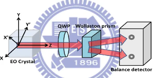
Fig. 2-1 Schematic figure of Electro-Optic Sampling
The principle can be explained as follow. Suppose z is the probe beam propagating direction, and x and y are the crystal axes of the EO crystal, respectively. When an electric field is applied to the EO crystal, the birefringence axes are induced by electric field x’ and y’ at an angle of with respect to x and y axes. If the input probe beam is polarized along x with amplitude, then the output beam can be expressed by
10
Where is the phase difference between the x’ and y’ polarizations, including dynamic term caused by THz field and static term, .
The intensity of probe beam in x and y direction can be expressed by
where is the input intensity and Ix+Iy=Io is the total energy. A Wollaston
prism is use to extract the and independently. A quarter-wave plate for balance detection that the static term is often set at . It’s operating at the linear region to avoid distortion. In the most cases of EO sampling, is much smaller than 1, so we can measure the signal and by a balance detector.
The signal difference that is proportional to the phase change
is
induced by THz field. Thus, we can obtain the total THz time-domain waveforms by measuring the signal difference via the balance detector as a function of delay time between the THz pulse and the laser probe pulse.11
2.3 - Time-Domain Measurement Technique
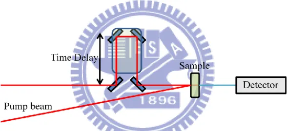
Pump-and-probe technique can be used to obtain the time-domain information on ultrafast phenomena. The general principles of pump-probe method need two ultrashort pulses: one is called “pump” beam which excites samples and the other one is called “probe” beam which can detect the temporal evolution of the perturbed sample. The time-resolved study of the photoexcited samples can be obtained by adjusting the time between pump and probe beamsThe single-cycle waveform of terahertz field can be obtained by this pump-and-probe method.
12
2.4 - Models and Analysis Methods
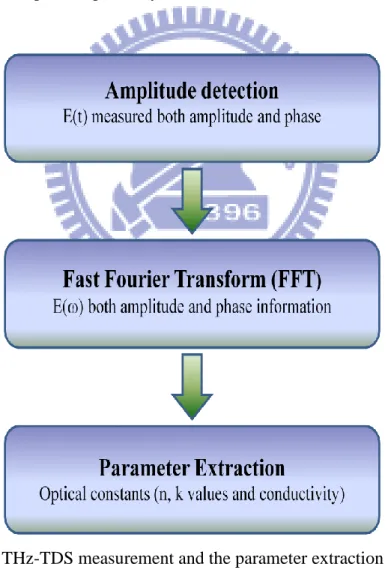
The THz time-domain spectroscopic (THz-TDS), both of frequency dependent amplitude and phase information can be obtained by Fast Fourier Transform (FFT). We can use these information to calculate the material’s frequency dependent optical constants of samples that including complex refractive index and conductivity without via Kramers-Kronig analysis. The information extraction process of time-domain spectroscopy is expressed as shown in Fig. 2-5. In this section, we will discuss the electromagnetic theories and analysis methods for two kinds of samples that are thick samples and thin samples, respectively.
13
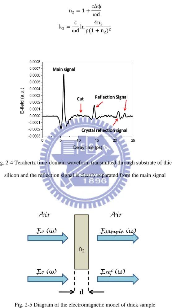
2.4.1 - Thick Samples
In general, the samples of thickness are hundred microns (typically 100m), the temporal terahertz reflection signal in time domain is clearly separated which caused by multiple reflections in the sample. We can reduce the reflection signal to simplify the analysis as show in Fig. 2.6. The schematic figure of the electromagnetic model is shown as Fig. 2.7, assuming normal and plane wave incidence. We assumed is the incident terahertz field, is the reference field, is the transmitted through the sample with thickness d, and c is speed of light in free space. and are refractive index for air and measured thick sample. The reference and signal field can be expressed by
Where and are transmission coefficient that is air (medium 1) to sample (medium 2) and sample to air, respectively. The formula can be expressed by
From above equations, the complex transmission coefficient of the sample can be expressed by
The complex transmission coefficient can be obtained from the Fast Fourier Transform (FFT) of experimental time-domain signals and . If
is much smaller than , we could ignore the influence of . Thus, complex refractive index can be obtained as
14
Fig. 2-4 Terahertz time-domain waveform transmitted through substrate of thick silicon and the reflection signal is clearly separated from the main signal
15
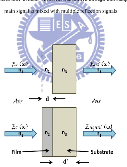
2.4.2 - Thin Samples
In general, the thickness of the samples was several micron meters or even only several hundred nanometers. So the reflection signal couldn’t be clearly separated in time-domain as shown in Fig. 2.8. The Fig. 2.9 illustrate with a schematic of the interaction of the THz pulse with sample. We assumed , , and be the incident THz field, the reference field through substrate with thickness d’ (substrate only), signal field transmitted through the thin film with thickness d and the signal field transmitted through both the thin film and substrate, respectively. In the formula, c is speed of light in free space. , and are refractive index for air, thin sample and thick substrate. and
is expressed as
We suppose a plane wave of impinging on the surface of the sample at normal incidence. Consider the multiple reflections within the thin film, can be represented by
Where q is the number of multiple reflections, and are Fresnel amplitude transmission and reflection coefficients which can be expressed by
16
Assuming the number of multiple reflections are infinite the
could be expressed as
The theoretical complex transmittance can be determined by
The transmission and reflection coefficients can be expressed by
The experimental data via the Fast Fourier Transform (FFT) that the time-domain signals are transformed into frequency domain. By dividing and , we obtained the experimental complex transmittance from THz-TDS data but there is no exact solution for the complex refractive index. For this goal, we use a numerical method and define an error function that can be expressed
If there exists a complex refractive index which makes the error function closest to zero at a part of frequency , we can extract the values at each frequency by use of mathematical program. We set a range of values for calculation and extract the best one that can makes the error function almost zero within them for each frequency to have the complex refractive index values.
17
Fig. 2-6 Terahertz time-domain waveform transmitted through thin samples and the main signal is mixed with multiple reflection signals
18
2.5 - Determination of Optical Conductivity and Mobility from
Drude Model and Drude Smith Model
In this section, we will discuss the optical conductivity and introduce Drude model and Drude-Smith model. From numerical methods discussed above, we have the frequency dependent complex refractive index of thin films. We can use the relation to obtain the frequency dependent complex optical conductivity. We start from Maxwell equation first of all. Assuming a simple conducting medium with flowing current, , and the formula can be expressed by
Where is the contribution of the bound electrons and is the effective dielectric constant. We can get by
and therefore the complex conductivity can be obtained from
The Drude model[25] was developed in the 1900s by Paul Drude that can be describe the transport properties of electrons in materials (especially metals). Consider the microscopic behavior of electrons in a solid as classical point electronic charges subject to random collisions that affect by an applied field. The classical simple Drude model that conductivity can be expressed by
19
The plasma frequency is defined by
, where N is carrier concentration, e
is the electronic charge, is the effective carrier mass and is carrier relaxation time. The DC conductivity is given by , where is carrier mobility. The simple Drude model indicates that the velocity of carriers is damped with a time constant and is randomized following each collision event. Many semiconductors in the terahertz region have been conform the simple Drude model, but still some materials, such as nanostructured materials cannot explain by simple Drude model.[26] Recently, Smith introduced a modified Drude model [27], which can explain the deviations from the simple Drude model, especially for the negative values of imaginary part of conductivity. Smith proposed the complex conductivity in the Drude-Smith model is given by
Where c is a parameter describing fraction of the electron’s original velocity after scattering and varied between -1 and 1. In the simple Drude model, the carrier is randomized after each scattering event, but in the Drude-Smith model, carriers retain a fraction c of their initial velocity. Mainly, c = 0 corresponds to the simple Drude conductivity and c = -1 means that carrier undergoes complete backscattering. The Drude-Smith model predicts a DC conductivity of and thus the reduced macroscopic DC mobility is given by .
20
Chapter 3 - Sample Properties
In this chapter, we describe the growth method and electric properties of a-plane and c-plane InN:Mg samples studied in this work.
3.1 - c-plane and a-plane InN and InN:Mg
Indium nitride (InN) is an interesting and potentially important semiconductor material with superior electric transport properties. Compared to all other group Ⅲ- Nitride, InN has small effective mass, high mobility and high saturation velocity. Therefore, it is very suitable for high speed and high frequency electronic device applications. The fundamental properties of InN are listed below.
InN Bandgap (eV) 0.7 Energy gap to next peak (eV) 2.8 Effective electron mass 0.07m0[28]
Mobility at 300k (cm2/Vs) 4000 Saturation speed (107cm/s) 4.2
Table 3-1 Physical properties of InN[29]
In this thesis report, a-plane and c-plane InN epitaxial films are studied. The crystal structure and atomic arrangement of a-plane and c-plane InN are shown in Fig. 3-1.In the c-plane InN film, the stacking series of its wurtzite structure is ABAB along the -c-axis direction.[30] In this growth direction, there are either In or N terminated polar surfaces in the surface layer and a-plane InN, both In and N exist along the surface. The built-in electric fields along the c-axis direction cause spatial separation of
21
electron and holes that in turn gives rise to restricted carrier recombination efficiency.[31-32] The wurtzite structure doesn’t have a mirror plane perpendicular to the c-axis and two surfaces can be defined by topmost single-broken-bond atom. The group Ⅲ- Nitride, such as In, Ga, or Al for cation-polarity ( ) plane and N for anion-polarity ( ) plane. Therefore, the polarization form anion-cation pair cannot disappearance by the inversion symmetry. In general, the growth direction along the c-axis called polar face and the a-axis or m-axis, we called non-polar face. Fig. 3-2 shows the atomic arrangement of InN along c- and a-plane [ ] and [ ] are crystal axis growth directions.
The thickness of InN films are in the range of 1-1.5 um. The c-plane { } undoped and Mg-doped InN epitaxial films with different concentrations were grown by plasma-assisted molecular beam epitaxy (PA-MBE) on Silicon (111) and the a-plane epitaxial films were grown on r-plane { } sapphire wafer. Mg doping was performed with a high-purity Mg (6N) Knudsen cell and the Mg doping level was controlled by resulting the cell temperature between 180 and 270℃. The electron concentrations and mobilities were determined by room-temperature Hall effect measurements. Fig. 3-3 is illustrated Magnesium cell temperature versus carrier concentration and Hall mobility.
22
Fig. 3-2 Atomic arrangement of InN along c- and a-plane [ ] and [ ] are crystal axis growth directions[7]
0 180 190 200 210 220 230 240 250 260 270 2.0x10¹⁷ 4.0x10¹⁷ 6.0x10¹⁷ 8.0x10¹⁷ 1.0x10¹⁸ 1.2x10¹⁸ 1.4x10¹⁸ 1.6x10¹⁸ 1.8x10¹⁸ 2.0x10¹⁸ 2.2x10¹⁸ c a rr ie r c o n c e n tr a ti o n (cm -3 ) Mg cell Temperature(oC) 0 200 400 600 800 1000 1200 H a ll m o b il it y ( cm 2 /V s )
Fig. 3-3 c-plane InN and InN:Mg Magnesium cell temperature versus carrier concentration and Hall mobility
23
c-InN and c-InN:Mg Sample Thickness (m) Mg cell Temp. (℃) Mobility (cm2/Vs) Concentration (cm-3) c-InN 091110 1.5 0 1120 2.0 x 10¹⁸ c-InN:Mg 080611 1.3 235 137 2.1 x 10¹⁸ c-InN:Mg 080525 1.0 195 176 1.6 x 10¹⁸ c-InN:Mg 090317 1.2 225 192 9.9 x 10¹⁷ c-InN:Mg 080624 1.2 225 530 4.3 x 10¹⁷
Table 3-2 List of c-plane and a-plane Undoped and Magnesium doped InN samples
a-InN Sample Thickness (m) Mg cell Temp. (℃) Mobility (cm2/Vs) Concentration (cm-3) a-InN 061229 (m-axis) 1.2 0 359 1.1 x 10¹⁹ a-InN 061229 (c-axis) 1.2 0 184 1.1 x 10¹⁹
24
Chapter 4 - Experimental Setups
In this chapter, we will introduce the laser system and our experimental THz-TDS systems (Electro-Optic THz system) used in this work.
4.1 - Femtosecond Laser System
In this work, we use two kinds of femtosecond laser systems that are oscillator titanium (Ti) sapphire laser and titanium (Ti) sapphire amplifier, respectively. The fundamental properties of two kinds of femtosecond laser systems are listed below.
Ti:Sapphire laser Regenerative amplifier Wavelength 800 nm 800 nm
Pulse Width 35 fs 50 fs
Repetition Rate 82 MHz 1 KHz
Energy 0.6 nJ 2 mJ
Polarization Vertical, linear Horizontal, linear Table 4-1 Properties of Ti-Sapphire laser and regenerative amplifier
25
The oscillator Ti:Sapphire laser (Tsunami, Spectra-Physics) is used as the seed laser that is pumped by a frequency-doubled diode-pumped Nd:YLF laser at 532nm with approximately 5W power (Millennia V). It can provide 35fs pulses with wavelengths ranging from 750 nm to 850 nm. The pulse repetition rate is ~82MHz and output power is up to 0.4W. The seed laser need stretched to avoid damaging the amplifier crystal and a Q-switched Nd:YLF laser (Empower) is used to pump the amplifier at 527nm with repetition rate is 1KHz and output power about 20W.. The pulse stretcher reduces the peak intensity and expending the pulse to several hundreds of picoseconds. After amplification, the amplified beam due to compressor and the beam’s pulse width compress about 50fs and output. This amplification process is called chirped pulse amplification. The pulse width of the Ti:sapphire regenerative amplifier (Spitfire, Spectra-Physics) beam is approximately 50fs with wavelength about 800nm. The repetition rate is 1KHz and provide the output power is about 2W corresponding to 2 mJ pulse energy.
4.2 - Experimental System
In this section, we will introduce our experimental system (Electro-Optic system). The setup of the Electro-Optic system is illustrated in Fig. 4-4. An amplified Ti:Sapphire laser providing 50fs, 800nm, 2mJ pulsed at repetition rate of 1KHz is used to drive this system. The linear s-polarized incident beam is divided into two separated beams by a beam splitter. The transmitted beam is used for the pump beam that to excite semiconductor to generating carriers and radiate THz pulse. The reflected beam is used as probe beam to detect the THz signal. We take the p-type InAs for emitter. Polarization of the pump beam is rotated to p-polarized by a half-wave plate (HWP). It’s used to generate p-polarized THz pulse in a
26
semiconductor surface emitter at the incident angle of 74.3 degrees to the surface normal which is close to Brewster angle. All the reflected laser beam from the emitter is blocked by a Teflon sheet which has a high transmission in the THz region. The generated THz radiation is collimated and focused onto the sample by a pair of silver-coated off-axis parabolic mirrors with focal 3 and 6 inches respectively. The transmitted THz radiation is again collimated and focused onto a 0.7-mm-thick (110) ZnTe crystal for free space electric-optic sampling by another pair of parabolic mirrors with the same focal lengths with previous pair. A pellicle beam splitter that is transparent to the THz beam and has a reflectivity of 5% for 800 nm light is used to make the probe beam collinear with the THz beam in the ZnTe crystal. The linear polarization of the probe beam is perpendicular to the polarization of the THz beam and we adjust the azimuth angle of the ZnTe crystal to achieve the highest modulation efficiency.
The evolution of the probe polarization is shown in series for the steps of the polarization manipulation with or without a THz field as shown in Fig. 4-3. The linear polarization of the probe beam without being modulated by THz radiation is converted to circular polarization and the probe beam modulated by the THz radiation is converted to ellipsoid polarization by a quarter-wave plate. After the quarter-wave plate, a Wollaston beam splitter is used to divide the modulated ellipsoid polarized probe beam into a linear s-polarized beam and p-polarized beam. A balanced detector with two photodiodes is used to detect the differential signal between two individual probe beams and the signal is proportional to the THz electric field. A motor stage within the probe beam path is used to scan the delay time between the probe pulse and the THz pulse imposing on the ZnTe crystal to obtain the entire THz time-domain waveform. In order to increase the signal to noise ratio (SNR), an optical chopper and a lock-in amplifier are used. The balance detector is connected to a lock-in amplifier
27
to amplify the signal and the signal can be obtained by a computer. The entire experimental setup is also located in a closed acrylic box for nitrogen purge which can decrease the environmental humidity to avoid the THz signal absorbed by water vapor.
Fig. 4-3 Probe polarization with and without a THz field are described before and after the polarization optics[33]
28
29
Chapter 5 - Experimental Results and Discussion
In this chapter, we first discuss the results of optical properties of InN:Mg samples measured by the electric-optical THz-TDS system. Afterward we discuss the a-plane experimental results. In this work, we can obtain all the transmittance of terahertz spectrum information.
5.1 - THz-TDS Measurement of c-plane InN and InN:Mg films
Undoped InN film
By using the THz-TDS system, the calculated of complex conductivity ( ) and refractive index ( ) can be studied from 0.3 to 2.1 THz. The details of sample description can be found in . For the parameter extraction, the temporal profiles of terahertz signal are recorded twice, the first time without the sample (only substrate), and the second time with the sample. The substrate of InN film is 370-m-thick silicon(111).
Figure 5-1(a) shows THz time domain waveforms with and without (in the free space) the silicon substrate. The amplitude and phase spectrums of air and silicon substrate are shown in Fig. 5-1 (b). The frequency dependent transmittance obtained via Fast Fourier Transform (FFT) is approximately 60% to 70% as shown in Fig. 5-1 (c). The extracted frequency-dependent refractive index and extinction coefficient (n and k value) are shown in Fig. 5-2 (a) and Fig. 5-2 (b), respectively. The frequency-dependent refractive index value of silicon is 3.4 which is the same as our previous result. Because the extinction coefficient (k value) is less than 0.05, it could be ignored for later calculation. After analysis of silicon substrate, we measured the terahertz time-domain spectrums of InN and InN:Mg samples. In the Fig 5-3 (a), the transmittance of InN film is about 20%.
30 0 3 6 9 12 15 -0.0004 -0.0002 0.0000 0.0002 0.0004 0.0006 0.0008 0.0010 0.0012 A m p li tu d e ( a .u .) Time delay (ps) Air Silicon
Fig. 5-1 (a) The terahertz time-domain signal transmitted through air and silicon
Fig. 5-1 (b) The corresponding amplitude and phase spectrums of air and silicon
0.0 0.5 1.0 1.5 2.0 2.5 3.0 0.00000 0.00001 0.00002 0.00003 0.00004 Frequency (THz) A m p li tu d e -100000 -50000 0 0.0 0.5 1.0 1.5 2.0 2.5 3.0 Air Silicon Frequency (THz) P h a s e
31 0.3 0.6 0.9 1.2 1.5 1.8 2.1 0.0 0.2 0.4 0.6 0.8 1.0 T ra n s m it ta n c e Frequency (THz)
Fig. 5-1 (c) The amplitude transmittance of silicon substrate
0.3 0.6 0.9 1.2 1.5 1.8 2.1 2.6 2.8 3.0 3.2 3.4 3.6 3.8 4.0 R e fr a c ti v e I n d e x n Frequency (THz)
32 0.3 0.6 0.9 1.2 1.5 1.8 2.1 0.00 0.05 0.10 0.15 0.20 E x ti n c ti o n c o e ff ic ie n t k Frequency (THz)
Fig. 5-2 (b) Frequency dependent extinction coefficient of silicon
0.3 0.6 0.9 1.2 1.5 1.8 2.1 0.0 0.2 0.4 0.6 0.8 1.0 T ra n s m it ta n c e Frequency (THz) 091110
33
The complex refractive index and conductivity of the InN film were calculated by using the methods at section 2.4 and are shown in Fig. 5-3 (b) and Fig. 5-3 (c), respectively. The frequency dependent conductivity results can be fitted theoretically by using the simple Drude model. The complex optical conductivity is defined by
The fit parameters, is the plasma frequency and is the carrier scattering time or called carrier damping rate. The fitting curves agree with the experimental data and two fitting parameters
40 THz and 49 fs were
obtained. The real conductivity of undoped indium nitride (091110 InN) decreases as the frequency increases, imaginary conductivity slowly increases. The best fitting curves for the real part and imaginary part of refractive index and conductivity are shown in Fig. 5-3 (c). Assuming an electron effective mass [34] for the undoped InN film, these fit parameters correspond to the carrier concentration about 1.5x1018 cm-3 and the carrier mobility 1155 cm2/V-s, in reasonable agreement with room-temperature electrical Hall effect measurement result of 2x1018 cm-3 and 1120.0 cm2/V-s.
34 0.3 0.6 0.9 1.2 1.5 1.8 2.1 0 5 10 15 20 25 30 35 40 R e fr a c ti v e i n d e x Frequency (THz) n k
Fig. 5-3 (b) Experimental data of refractive index and extinction coefficient of InN film 0.3 0.6 0.9 1.2 1.5 1.8 2.1 -100 -50 0 50 100 150 200 250 300 350 400 450 C o n d u c ti v it y (cm -1 O -1 ) Frequency(THz) Real Imaginary
Fig. 5-3 (c) Experimental data (open symbols) and fitting data complex conductivity (solid line) of InN film
35
Mg-doped InN film
Fig. 5-4 (a) shows the terahertz time-domain waveform of silicon substrate and the c-InN:Mg film. The amplitude and phase spectrums of silicon substrate and InN:Mg film are shown in Fig 5-4 (b). The transmittance of undoped InN film is less than 20%, whereas that of doping magnesium acceptors into InN films enhances the transmittance of terahertz around three times (>60%). Fig. 5-5 (c), (d), (e), and (f) are show the transmittance of each sample with different carrier concentration N from 4.3x10¹⁷ to 2.1x1018 cm-3. Interestingly, we found the terahertz transmittance does not have particular dependence on carrier concentration. After doping magnesium acceptors, acceptors and carries are to combine in the semiconductor. Thus all the transmittance of InN doping magnesium films are increase that indicates the conductivity were decrease. First, it is seen InN:Mg film with Hall measurement of carrier concentration (N=2.1x1018 cm-3) has similar to that of undoped InN film, but the transmittance is three times higher than that of undoped InN film. It is clearly indicating doping the magnesium acceptors affect the material property of InN semiconductor.
Fig 5-5 to 5-8 show the complex refractive index ( ) and optical conductivity ( ) of four selected c-InN:Mg films with different carrier concentrations. The calculated results shows the conductivity of imaginary part is almost zero for the c-InN:Mg films. The carrier concentration of each sample measured by Hall measurement is 2.1x10¹⁸, 1.6x10¹⁸, 9.9x10¹⁷, and 4.3x1017 cm-3, respectively. Despite of different carrier concentration, all the four samples of c-InN:Mg have a nearly frequency-independent conductivity of ~50cm-1Ω-1. This result can be fitted theoretically by using the simple Drude model. With the assumption of me=0.075m0, the whole best fitting parameters and are given in
36 Table 5-1. 0 5 10 15 20 25 -0.0002 0.0000 0.0002 0.0004 0.0006 0.0008 A m p li tu d e ( a .u .) Time delay (ps) Silicon InN:Mg
Fig. 5-4 (a) The terahertz time-domain signal transmitted through silicon and InN:Mg
Fig. 5-4 (b) The corresponding amplitude and phase spectrums of silicon and InN:Mg
0.0 0.5 1.0 1.5 2.0 2.5 3.0 0.000000 0.000005 0.000010 0.000015 0.000020 0.000025 Silicon InN:Mg Frequeancy (THz) A m p li tu d e -100000 -80000 -60000 -400000.0 0.5 1.0 1.5 2.0 2.5 3.0 Frequeancy (THz) P h a s e
37 0.3 0.6 0.9 1.2 1.5 1.8 2.1 0.0 0.2 0.4 0.6 0.8 1.0 T ra n s m it ta n c e Frequency (THz) 080611
Fig. 5-4 (c) The amplitude transmittance of InN:Mg film (N=2.1x1018 cm-3)
0.3 0.6 0.9 1.2 1.5 1.8 2.1 0.0 0.2 0.4 0.6 0.8 1.0 T ra n s m it ta n c e Frequency (THz) 080525
38 0.3 0.6 0.9 1.2 1.5 1.8 2.1 0.0 0.2 0.4 0.6 0.8 1.0 T ra n s m it ta n c e Frequency (THz) 090317
Fig. 5-4 (e) The amplitude transmittance of InN:Mg film (N=9.9x1017 cm-3)
0.3 0.6 0.9 1.2 1.5 1.8 2.1 0.0 0.2 0.4 0.6 0.8 1.0 T ra n s m it ta n c e Frequency (THz) 080624
39 0.3 0.6 0.9 1.2 1.5 1.8 2.1 -60 -40 -20 0 20 40 60 80 100 C o n d u c ti v it y (cm -1 O -1 ) Frequency (THz) Real Imaginary
Fig. 5-5 (a) Experimental data (open symbols) and fitting data complex conductivity (solid line) of InN:Mg film (080611 | N=2.1x1018 cm-3)
0.3 0.6 0.9 1.2 1.5 1.8 2.1 0 2 4 6 8 10 12 14 16 18 20 R e fr a c ti v e i n d e x Frequency (THz) n k
Fig. 5-5 (b) Experimental data of refractive index and extinction coefficient of InN film (080611 | N=2.1x1018 cm-3)
40 0.3 0.6 0.9 1.2 1.5 1.8 2.1 -60 -30 0 30 60 90 120 150 Real Imaginary C o n d u c ti v it y (cm -1 O -1 ) Frequency (THz)
Fig. 5-6 (a) Experimental data (open symbols) and fitting data complex conductivity (solid line) of InN film (080525 | N=1.6x1018 cm-3)
0.3 0.6 0.9 1.2 1.5 1.8 2.1 0 4 8 12 16 20 R e fr a c ti v e i n d e x Frequency (THz) n k
Fig. 5-6 (b) Experimental data of refractive index and extinction coefficient of InN film (080525 | N=1.6x1018 cm-3)
41 0.3 0.6 0.9 1.2 1.5 1.8 2.1 -40 -20 0 20 40 60 80 Real Imaginary C o n d u c ti v it y (cm -1 O -1 ) Frequency (THz)
Fig. 5-7 (a) Experimental data (open symbols) and fitting data complex conductivity (solid line) of InN:Mg film (090317 | N=9.9x1017 cm-3)
0.3 0.6 0.9 1.2 1.5 1.8 2.1 0 2 4 6 8 10 12 14 16 R e fr a c ti v e i n d e x Frequency (THz) n k
Fig. 5-7 (b) Experimental data of refractive index and extinction coefficient of InN film (090317 | N=9.9x1017 cm-3)
42 0.3 0.6 0.9 1.2 1.5 1.8 2.1 -40 -20 0 20 40 60 80 100 Real Imaginary C o n d u c ti v it y (cm -1 O -1 ) Frequency (THz)
Fig. 5-8 (a) Experimental data (open symbols) and fitting data complex conductivity (solid line) of InN:Mg film (080624 | N=4.3x1017 cm-3)
0.3 0.6 0.9 1.2 1.5 1.8 2.1 0 4 8 12 16 20 R e fr a c ti v e i n d e x Frequency (THz) n k
Fig. 5-8 (b) Experimental data of refractive index and extinction coefficient of InN film (080624 | N=4.3x1017 cm-3)
43
(c-plane InN and InN:Mg)
Parameters comparison of Hall effect measurement and TDS fitting by Drude model Sample p / 2 (THz) 0 (fs) N (TDS) (x1018 cm-3) N (Hall) (x1018 cm-3) (TDS) (cm-2 /V-s) (Hall) (cm-2 /V-s) InN (091110) 40 49 1.5 2.0 1155 1120 InN:Mg (080611) 36 9 1.2 2.1 204 137 InN:Mg (080525) 39 11 1.4 1.6 255 176 InN:Mg (090317) 28 12 0.7 1.0 287 192 InN:Mg (080624) 21 34 0.4 0.4 747 530
Table 5-1 Parameters comparison of Hall effect measurement and TDS fitting by Drude model
44
5.2 - Discussion of c-InN:Mg results
Our calculated carrier concentrations of all the InN:Mg films in Table 5-1 that agree well with those obtained by Hall measurement. The consistency of the results between Hall effect measurement and THz-TDS has an important implication that are n-type conductivity of InN:Mg films measured by Hall effect measurement may represent the electrical property of the whole film. In contrast, if we change to the hole effective mass ( ) to calculate the conductivity that is assumed the p-type conductivity of InN:Mg.[35][36] Thus the corresponding carrier concentration of each InN:Mg film can be much higher than the electron concentration and mobility lower than carrier mobility measured by Hall effect measurement. Despite the THz-TDS method cannot clearly make sure the type of semiconductor. Nontheless, we use electron effective mass to calculate the carrier concentration and carrier mobility are similar Hall effect measurement that may indicate our result is n-type semiconductor.
In Table 5-1, we found that the fitting of carrier scattering times of the InN:Mg films in our results are significantly reduced compared to undoped to that of undoped InN film. This result shows that magnesium doping induces the reduction of the conductivity and refractive index reduction. For semiconductor, the major contribution to the scattering time includes below:[37]
phonons:both acoustic and optical ionized impurities
neutral defects
other carriers (e. g. scattering between electrons and holes)
The photoluminescence (PL) intensity of the InN:Mg films is typically much weaker than that of undoped InN, implying the inferior crystalline quality of InN:Mg films
45
combined with impurities, defects, and dopants during the film growth.[38] A first-principles study also shows that dopants like magnesium in InN create the deep formation energy and magnesium acceptors substituted on In or N sites lead to the reduction in local symmetry associated with the relative positions of magnesium dopant and provide the scattering centers.[39] In addition, doped semiconductors, which are typically ionized, are charged and higher ionized impurity scattering slao occurs for highly doped semiconductor. Therefore, it clearly that impurity or defect scattering introduced by magnesium doping shortens the scattering time in the InN:Mg film and consequently leads to the terahertz transparency accompanied by low conductivity.
46
5.3 - THz-TDS Measurement of a-plane InN film
In this section, we will discuss the a-plane InN film experimental data. The substrate of a-plane InN film is grown on r-plane { } sapphire and the thickness is approximately 430-um-thick. Fig. 5-9 (a) and Fig. 5-9 (b) show the crystal structure of sapphire. We know sapphire is an anisotropic material, rhombohedral crystal structure. If the wave incidence to an anisotropic material that brings the birefringence. Because the anisotropic medium supports two modes with distinctly different phase velocities, therefore we can obtain different refractive index.
Fig. 5-9 (a) The crystal structure of sapphire
(http://www.namiki.net/product/jewel/sapphire/index.html)
47
Fig. 5-10 (a) shows the terahertz time-domain waveforms of sapphire substrate with different polarization field which are c-axis perpendicular and parallel terahertz wave, respectively. The time-domain terahertz signals of ordinary and extraordinary rays have different time delay. The amplitude and phase spectrums of air and sapphire substrate are shown in Fig. 5-10 (b). The transmittance of sapphire substrate obtained via Fast Fourier Transform (FFT) is approximately 70% as shown in Fig. 5-10 (c). The extracted frequency-dependent refractive index and extinction coefficient (n and k value) are shown in Fig. 5-10 (d) and Fig. 5-2 (e), respectively. The frequency-dependent refractive index value of sapphire is approximate 3.32 and 3.10 as terahertz field is parallel and perpendicular to c-axis, respectively and the extinction coefficient (k value) both orientations are approximately 0 (<0.02).
0 2 4 6 8 10 12 14 16 -0.0008 -0.0006 -0.0004 -0.0002 0.0000 0.0002 0.0004 0.0006 0.0008 0.0010 0.0012 0.0014 0.0016 A m p li tu d e ( a .u .) Time delay (ps) Air E c-axis E c-axis
Fig. 5-10 (a) The terahertz time-domain signal transmitted through air and sapphire with electric field perpendicular and parallel c-axis
48
Fig. 5-10 (b) The corresponding amplitude and phase spectrums of air and sapphire substrate with electric field perpendicular and parallel c-axis
0.3 0.6 0.9 1.2 1.5 1.8 2.1 0.0 0.2 0.4 0.6 0.8 1.0 T ra n s m it ta n c e Frequency (THz) E c-axis E c-axis
Fig. 5-10 (c) The amplitude transmittance of sapphire substrate with electric field perpendicular and parallel c-axis
0.0 0.5 1.0 1.5 2.0 2.5 3.0 0.00000 0.00002 0.00004 0.00006
Frequency (THz)
A
m
p
li
tu
d
e
-100000 -50000 0 0.0 0.5 1.0 1.5 2.0 2.5 3.0 Air E c-axis E c-axis P h a s e49 0.3 0.6 0.9 1.2 1.5 1.8 2.1 3.0 3.1 3.2 3.3 3.4 3.5 E c-axis E c-axis R e fr a c ti v e I n d e x n Frequency (THz)
Fig. 5-10 (d) Frequency dependent refractive index of sapphire with electric field perpendicular and parallel c-axis
0.3 0.6 0.9 1.2 1.5 1.8 2.1 0.00 0.05 0.10 0.15 0.20 0.25 0.30 R e fr a c ti v e I n d e x k Frequency (THz) E c-axis E c-axis
Fig. 5-10 (e) Frequency dependent extinction coefficient of sapphire with electric field perpendicular and parallel c-axis


![Fig. 1-2 The energy band gaps of Group -Ⅲ Nitride semiconductors [7]](https://thumb-ap.123doks.com/thumbv2/9libinfo/8241415.171341/15.892.245.651.397.756/fig-energy-band-gaps-group-nitride-semiconductors.webp)
![Table 3-1 Physical properties of InN [29]](https://thumb-ap.123doks.com/thumbv2/9libinfo/8241415.171341/31.892.166.633.491.821/table-physical-properties-of-inn.webp)
![Fig. 3-1 Crystal structure of InN [8]](https://thumb-ap.123doks.com/thumbv2/9libinfo/8241415.171341/32.892.320.571.881.1077/fig-crystal-structure-of-inn.webp)
