氮化矽記憶元件內電荷分佈與可靠性分析
63
0
0
全文
(2) 氮化矽記憶元件內電荷分怖與可靠性分析 Localized Charge Distribution and Read Current Noise in Nitride Storage Flash Cells. 研 究 生 : 王銘德. Student : Ming-Te Wang. 指導教授 : 汪大暉 博士. Advisor : Dr. Tahui Wang. 國立交通大學 電子工程學系 電子研究所碩士班 碩士論文. A Thesis Submitted to Institute Electronics College of Electrical Engineering and Computer Science National Chiao Tung University in Partial Fulfillment of the Requirements for the Degree of Master of Science in Electronic Engineering June 2004 Hsinchu, Taiwan, Republic of China.. 中華民國 九十三 年 六 月.
(3) 氮化矽記憶元件內電荷分佈與可靠性分析. 學生:王銘德 國立交通大學. 指導教授:汪大暉 博士 電子工程學系. 電子研究所. 摘要. 本篇論文主要著重於氮化矽記憶元件內儲存電荷分怖以及讀取電流不穩定 等可靠性議題之討論。這些可靠性議題主要包括:寫入狀態電荷之橫向分佈 (program charge lateral spread)、寫入動作干擾(program disturb effect)、以及讀 取電流雜訊(read current noise)。而在此研究中,氮化矽記憶元件為一 n 型通道 金氧半場效電晶體包含一 ONO 閘極結構。 由於雙位元操作,逆向讀取第二位元之臨界電壓時,可能受到第一位元儲存 電荷的干擾,故控制儲存電荷分佈為一重要可靠性議題,我們以電荷幫浦方法 (charge pumping)得以一窺氮化矽層中儲存電荷之分佈情形。此外,建立一套微秒 暫態量測電路(micro-second transient measurement circuit),藉著此電路的輔助, 我們將得以觀測短時間因寫入動作干擾所引發的可靠性議題,並研究因隨機雜訊 所引發之讀取電流不穩定,此一不穩定現象會隨著寫入/抹除次數增加和閘極長度 微縮而變差。且利用通道熱電子所寫入之不均勻電荷分佈亦會擴大其效應。憑藉 在本篇論文中所提及之氧化層改進方法,此種負面現象將得以舒緩。. i.
(4) Localized Charge Distribution and Read Current Noise in Nitride Storage Flash Cells. Student: Ming-Te Wang. Advisor: Dr. Tahui Wang. Department of Electronics Engineering & Institute of Electronics National Chiao Tung University. Abstract. This thesis will focus on the discussion of localized trapped charge distribution in nitride film and read current instability issue in a SONOS type flash memory cell, which include program charge lateral spread, program disturb effect, and read current noise. In this study, the flash memory cell is made of a n-channel MOSFET with an oxide-nitride-oxide gate structure. For two-bit storage, the control of programmed charge lateral distribution is particularly important since stored electrons at the first bit will affect the threshold voltage of the second bit in reverse read. We use a charge pumping method to explore the programmed charge distribution of each bit. In addition, a micro-second transient measurement circuit is set up to investigate the program disturb effect. Furthermore, program/erase cycling induced random. ii.
(5) telegraph noise in read current noise is observed. The amplitude of current fluctuation increases with P/E cycle number and with decreasing gate length. Non-uniform charge storage by CHE programming can further enhance read current fluctuation. The improvement of bottom oxide reliability can significantly reduce this effect.. iii.
(6) 致謝 人生的每一個遭遇,都是我們最真實的存在 首先,這本碩士論文的完成,必須感謝汪大暉教授的指導與鼓 勵,他紮實且深入的研究訓練,使我面對未來的挑戰更有信心。 論文研究上感謝小兔學長一年多來無私的教誨,細心與耐心的教 導,使我很容易對實驗上手,並有效率學習到新的知識及觀念。另外, David 學長的嚴謹治學與實事求是,令我受用無窮。 成長,就是尋找自己的旅程。感謝曾經一同走過的許多學長,及 參與研究的同學。首先感謝蔡慶威、吳俊威學長在研究生活中的鼓勵 與指導;感謝小凱、小翎學長、及兆琪學姐,有你們的陪伴,在嚴肅 的學問鑽研中增添輕鬆愉悅的氣氛。學識上的傾囊相授與人生經驗的 交流,特別感謝陳旻政學長,由衷地。感謝志昌、建文、子強、信榮、 政賢及文雄的陪伴,一起走過精彩的兩年。 最後,感謝我的父母、家人,在求學其間給我的鼓勵和支持,有 他們在背後無怨無悔的付出與關心,讓我毫無顧忌的專注於論文研 究。 五十多頁的文字,承載七百多個日子滿滿的回憶。. iv.
(7) Contents Chinese Abstract English Abstract Acknowledgements Contents Figure Captions Chapter 1 Introduction Chapter 2 Programmed Charge Lateral Spread 2.1. Introduction. 2.2. Charge Pumping measurement. 2.3. Programmed Charge Distribution 2.3.1 First Bit Icp 2.3.2. Two Bit Storage Icp. 2.4. Simulation of the Channel Field distribution. 2.5. Cycling Dependence. Chapter 3 Program Disturb Induced Erase State Vt Shift 3.1. Introduction. 3.2. Micro-Second Transient Measurement. 3.3. PCAT Model. 3.4. Program Disturb Behavior 3.4.1 Measurement Setting 3.4.2 Program-disturb Characteristics 3.4.3 Cycling Dependence 3.4.4 Summary. 3.5. Modified Erase Scheme. v. i ii iiv v vii 1 6 6 6 7 7 14 14 15 22 22 22 23 23 23 29 29 29 30.
(8) Chapter 4. P/E Cycling Induced Read Current Noise. 4.1. Introduction. 4.2. Random Telegraph Noise Measurement. 4.3. P/E Cycling Stress. 4.4. Length Dependence & Non-uniform Vt Effect. 4.5. Oxide Process Effect. Chapter 5 Reference. Conclusion. vi. 35 35 35 36 36 43 46 47.
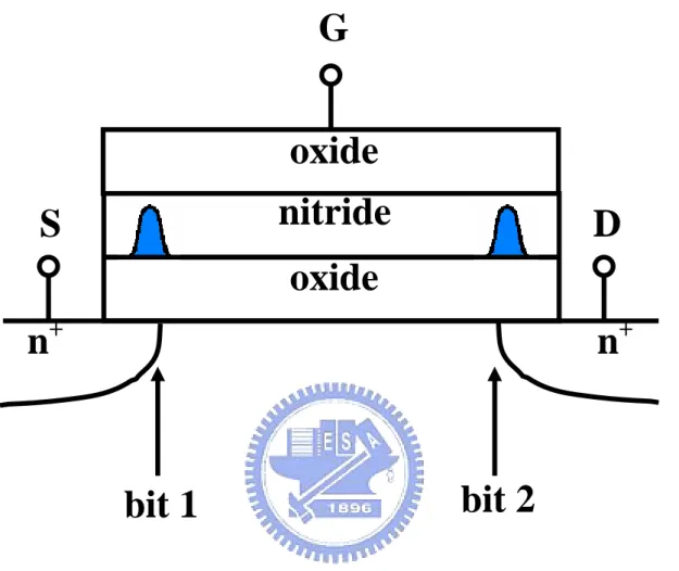
(9) Figure Captions Fig. 1.1. Schematic representation of a SONOS cell and two-bit storage. The shaded area in the nitride layer represents stored charges.. Table 1.1 Suggested bias conditions for MXVAND cell operation. Fig. 1.2. Drain current versus gate bias in erase state and in program state.. Fig. 2.1. Schematic diagram of a two-bit storage nitride cell and a CP measurement setup. The dashed line in the substrate represents the depletion region caused by Vd. The thickness of the ONO gate stack is 9nm (top oxide), 6nm and 6nm, respectively. Fig. 2.2. Schematic illustration of Vgl varying CP measurement. Vgh is above Vt and varying. Vgl. probed.. The. part. of. channel. undergoes. the. accumulation-inversion-accumulation contributes the Icp (bulk current). Fig. 2.3. Icp versus Vgl in a fresh cell, in program state, and in erase state, respectively. The Vt window (∆Vt) is 2V. Vd in CP measurement is 0V.. Fig. 2.4. The program-state Icp bump increases with Vt window due to more injected charges.. Fig. 2.5. The decrease of the program state Icp bump with Vd in CP measurement. The Vt window is 2V.. Fig. 2.6. The program state Icp measured at Vd=1.8V & Vs floating and Vs=1.8V & Vd floating.. Fig. 2.7. The Icp of the four states of two-bit storage. “11” represents both bits in erase-state and “10” represents one bit in erase-state and one bit in program-state.. Fig. 2.8. Comparison of the Icp of the first programmed bit and the secondly programmed bit. The 2nd bit Icp is measured with the first bit erased.. vii.
(10) Fig. 2.9. Lateral profiling of the programmed charge distribution of the 1st programmed bit and the 2nd programmed bit. An uniform interface trap distribution along the channel is assumed. Icp,max is 195pA.. Fig. 2.10 Calculated channel field distribution in 2nd bit programming from 2D device simulation. x=0 is at the n+ source edge and x=0.4 is at the n+ drain edge.Vs=6.5V and Vg=11V in 2nd bit programming. Fig. 2.11 The difference in Icp between program state and erase state as a function of drain bias for the 1st bit and source bias for the 2nd bit. ∆Icp is obtained from Fig. 2.8 at Vgl=1.6V. Fig. 2.12 The difference in Icp between program state and erase state as a function of Vd in CP measurement at various P/E cycle numbers. ∆Icp is measured at Vgl= 1.6V and is normalized to its value at Vd=0V to take into account interface trap creation in cycling. Fig. 3.1. Scheme of the virtual ground array and a technique to inhibit program disturb in adjacent cell. Programming D-bit of Cell P, program disturbs in Cell N with the same WL voltage (11V).. Fig. 3.2. Circuit diagram of micro-second measurement system. The applied bias of P/E phase and M/D phase are shown in the table.. Fig. 3.3. Photograph of our micro-second transient measurement circuit.. Fig. 3.4. Illustration of positive oxide charge assisted tunneling current (Isd). The time-dependence of Isd and corresponding Vt shift was gived.. Fig. 3.5. The applied waveform patterns. The resolution of the measurement and disturb phase is 200µs. Fig. 3.6. Program and read disturb characteristics of a 10K P/E cell. Lg=0.5µm.. Fig. 3.7. Vt shift versus wait time intermediately after erase. Applied Vg=Vd=Vs=Vb=0V during the wait time.. viii.
(11) Fig. 3.8. Cycle number dependence of Vt shift. Note that no Vt shift at a fresh cell and after 10K P/E cycles there is a 0.17V Vt shift during 100ms stress.. Fig. 3.9. Vt shift of conventional erase and with electrical anneal step erase. The anneal step is Vg/Vd=10/4V with 10K cycled cell.. Fig. 4.1. Experimental setup for RTN measurement.. Fig. 4.2. Representative RTN traces in a NROM cell (W/L=0.35µm/0.3µm). (a) fresh, (b) 1k P/E cycles, (c) 100k P/E cycles.. Fig. 4.3. Comparison of RTN amplitude in program-state and in erase-state (b) Dependence of ∆Id (two-level transition) on read current. The P/E cycle number is 100 P/E. The reverse read bias is Vg=4V, Vs=1.5V and Vd=0V.. Fig. 4.4. (a) Comparison of RTN amplitude for Lg=0.3µm and 0.5mm. (b) Dependence of ∆Id (two-level transition) on gate length. The read current level is about 1µA.. Fig. 4.5. Calculated gate length dependence of two-level RTN amplitude from 2D device simulation. For CHE injection, the trapped charge width is assumed to be 30nm. FN injection has uniform charge storage. The parameters in simulation are not calibrated.. Fig. 4.6. Typical RTN traces for uniform FN injection (a) and channel hot electron injection (b). Both cells have the same P/E stress conditions.. Fig. 4.7. Maximum ∆Id observed at a read current of 30µA from multi-level RTN. The sampling size is 105 readings.. Fig. 4.8. (a) The increment of charge pumping current (Icp) in device A and device B after 10k P/E cycles. (b) RTN traces in Device A after 10k P/E cycles (c) RTN traces in Device B after 10k P/E cycles. ix.
(12) Chapter 1 Introduction Currently, two major research thrusts in nonvolatile semiconductor memory are underway. One has data stored in a multi-layer gate structure in a field effect transistor and the other takes advantage of electrical polarization of ferroelectric material in a ferroelectric capacitor/transistor [1]. With respect to charge storage devices, there are two kinds of them. (a) Charge Trapping Devices: Charge is stored in traps at the interface of a multi-layer gate structure and/or in the bulk of insulator, such as the metal nitride oxide silicon (MNOS) structure [2], [3]. (b) Floating Gate Devices: Charge is stored in a thin conducting or semiconductor layer or conducting particles sandwiched between insulators [4], [5]. However, since its invention in 1967, the nitride-based nonvolatile memory structures, both MNOS and polysilicon oxide-nitride-oxide silicon (SONOS) [6]-[10], have received limited commercial acceptance due to their employment of ultra-thin dielectric (~20Å) and their non-ideal charge retention characteristics. In conventional SONOS cells, charges are stored uniformly in the nitride layer. This SONOS concept has recently evolved into a two-bit storage cell (NROM). Recently, the new SONOS flash EEPROM cell has soon gained great attention for their smaller size per bit (2.5F²/bit in Flash, where F is the feature size of the process) [11], [12], less fabrication complexity [13], no drain turn-on and better charge retentivity [14] This SONOS cell is made of a n-channel MOSFET with an oxide-nitride-oxide gate dielectric structure, as shown in Fig.1.1. The major difference between NROM and the conventional SONOS devices [15] is that the bottom oxide is about 60Å [11], which is much thicker than that of SONOS (~20 Å), where direct tunneling is involved for charge transport. By taking advantage of localized charge storage in the nitride layer above the n+. 1.
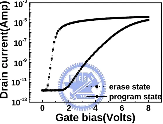
(13) source and drain junctions, two-bit per cell operation can be achieved. Channel hot electron injection and band-to-band hot hole injection are utilized for programming and erasing, respectively. Table.1.1 shows the operation bias of program, erase, and read [16]. The Id-Vgs of program state and erase state are shown in Fig.1.2 by using a reverse read method [17], which can be used to “read through” the first bit to obtain the information of the second bit. The sub-threshold swing deterioration in program state is due to a narrow charge trapping region, typically tens of nano-meter. Because of a thicker bottom oxide and the non-uniformity of charge stored in the nitride layer, the reliability issues in the two-bit storage SONOS cell are quit different from that in the conventional SONOS cells. Charge loss characteristics and cycling endurance of these kind of cells have been discussed, and the models have been proposed [16], [18]-[22]. Following the introduction, the programmed charge lateral spread in the nitride layer will be discussed in chapter two. In chapter three, we will demonstrate a micro-second transient measurement circuit to investigate program disturb effect. Random telegraph noise induced read current fluctuation will be discussed in chapter four. Finally, we will make a conclusion of this thesis.. 2.
(14) G oxide nitride. S. D. oxide n+. n+. bit 2. bit 1. Fig. 1.1. Schematic representation of a SONOS cell and two-bit storage. The shaded area in the nitride layer represents stored charges.. 3.
(15) Table.1.1. Bit 1. Bit 2. Suggested bias conditions for MXVAND cell operation.. Program. Erase. Read. Vg. 11V. -3V. 2.5V. Vd. 5V. 8V. 0V. Vs. 0V. 0V. >1.5V. Vg. 11V. -3V. 2.5V. Vd. 0V. 0V. >1.5V. Vs. 5V. 8V. 0V. 4.
(16) Drain current(Amp). -3. 10. -5. 10. -7. 10. -9. 10. -11. 10. -13. 10. 0. 2. 4. erase state program state 6 8. Gate bias(Volts). Fig. 1.2. Drain current versus gate bias in erase state and in program state.. 5.
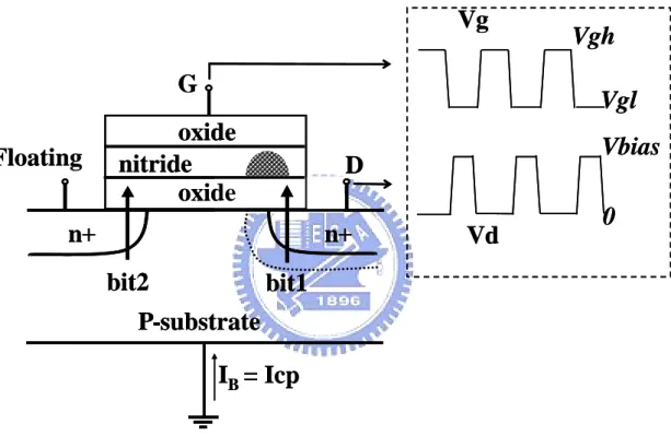
(17) Chapter 2 Programmed Charge Lateral Spread 2.1 Introduction NROM flash cells have received much interest recently due to their smaller bit size, simpler fabrication process and absence of drain induced turn-on. By taking advantage of localized charge trapping in nitride above the source and the drain junctions, two-bit storage of a nitride cell can be achieved by utilizing hot electron program and band-to-band hot hole erase with a reverse read scheme. For two-bit storage, the control of programmed charge lateral distribution is particularly important. This is because that in 2-bit operation, the stored electrons at the first bit will affect the threshold voltage of the second bit in reverse read and vice versa [23]. Furthermore, the lateral spread of programmed charge will cause a mismatch between programmed electron distribution and injected hole distribution in erase operation, thus resulting in the degradation of erase capability or ease speed [24]. In this work, we will use a modified charge pumping technique to explore the programmed electron distribution in the nitride layer. Moreover, we find that the programmed charge distribution spreads further into channel with program/erase cycle number. Finally, by using this profiling technique, the lateral spread of the first and secondly programmed bits can be characterized, and the cycling induced charge distribution broadening will be investigated.. 2.2 Charge Pumping Measurement The voltage waveforms in our charge pumping (CP) measurement are illustrated in Fig 2.1. We use trapezoidal gate pulses with a fixed Vgh and varying Vgl. The substrate current (called “charge pumping current (Icp)”) versus Vgl is measured. The. 6.
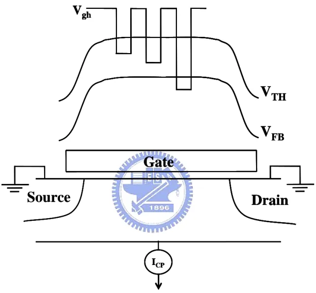
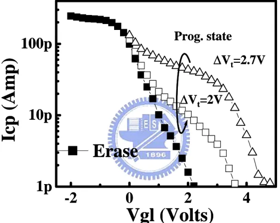
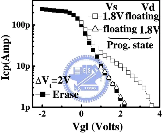
(18) fixed Vgh is sufficiently high to ensure that the entire channel is inverted [26]- [29]. By varying Vgl, only the part of channel where Vt is lower than Vgh can contribute to Icp (Fig 2.2). When the entire channel contributes to the charge pumping current, Icp reaches its maximum value. Vd is adjusted to modulate the drain (or source) depletion width while Vs is floating. The gate pulses have a frequency of 2.5 Mhz and 50% duty cycle. Rising and falling times are 2ns. The samples used in this work have a gate width of 0.35µm and a gate length of 0.5µm.. 2.3 Programmed Charge Distribution 2.3.1 First bit Icp Fig 2.3 shows Icp versus Vgl with Vd=0V and source is floating in a fresh cell, in program state and in erase state, respectively. Only the first bit (drain side) is P/E cycled. The threshold voltage window (∆Vt) is 2V. Here, Vt is defined as the gate voltage when the drain current is 1µA at a reverse read voltage of 1.6V. Note that Icp in a fresh cell and in erase state are almost identical. The negative charge trapping is reflected by an Icp bump in program state. The maximum Icp (Icp,max) bump is 195pA at Vgl=0V in Fig 2.3. The interface trap density (Nit) can be extracted by Eq. (2.1).. I cp , max = qfN itWLg. (2.1). where q is the elementary charge, f the gate pulse frequency, W the effective channel width, and Lg is the gate length. The program state Icp bump increases with the Vt window because of more injected charges in the ONO layer (Fig 2.4). The dependence of the program state Icp bump on applied drain bias in charge pumping measurement is shown in Fig 2.5. When a low drain bias is applied, traps underneath the programmed charge are partly masked by the drain depletion region. At a sufficiently large Vd, for example 1.8V, the program state Icp bump is completely suppressed. In contrast, when a Vs is applied in charge pumping measurement, the Icp. 7.
(19) Vg G Floating. Vgh Vgl. oxide nitride oxide. n+. n+ bit2. Vbias. D Vd. 0. bit1. P-substrate IB = Icp. Fig. 2.1 Schematic diagram of a two-bit storage nitride cell and a CP measurement setup. The dashed line in the substrate represents depletion region caused by Vd. The thickness of the ONO gate stack is 9nm (top oxide), 6nm and 6nm, respectively.. 8.
(20) Vgh gl. VTH VFB Gate Source. Drain. ICP. Fig. 2.2 Schematic illustration of Vgl varying in CP measurement. Vgh is above Vt and Vgl is varying. The part of channel undergoing accumulation-inversion-accumulation contributes to the Icp (bulk current). 9.
(21) Icp(Amp). 100p. 10p. 1p. Nitride charge trapping. ∆Vt=2V. fresh Prog. state Erase state -2. 0. 2. 4. Vgl(Volts) Fig. 2.3. Icp versus Vgl in a fresh cell, in program state, and in erase state, respectively. The Vt window (∆Vt) is 2V. Vd in CP measurement is 0V.. 10.
(22) Prog. state. Icp (Amp). 100p. ∆Vt=2.7V ∆Vt=2V. 10p. Erase 1p. -2. 0. 2. 4. Vgl (Volts) Fig. 2.4. The program-state Icp bump increase with Vt window due to more injected charges. 11.
(23) Icp (Amp). 100p. Vd 0V 0.8V 1.8V. Prog. state. 10p. ∆Vt=2V. Erase 1p. -2. 0. 2. Vgl (Volts) Fig 2.5. The decrease of the program state Icp bump with Vd in CP measurement. The Vt window is 2V.. 12. 4.
(24) Vs Vd 1.8V floating floating 1.8V. Icp(Amp). 100p. Prog. state 10p. ∆Vt=2V. Erase 1p. -2. 0. 2. Vgl (Volts) Fig 2.6. The program state Icp measured at Vd=1.8V & Vs floating and Vs=1.8V & Vd floating.. 13. 4.
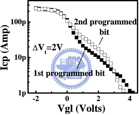
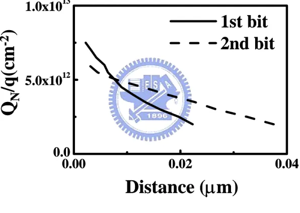
(25) bump is not affected at all (Fig 2.6). The drain pulse is 180o phase-shifted with respect to Vg that the drain bias is applied only during the trapped electron emission cycle [29]. This indicates that the programmed charge is highly localized near the drain edge. 2.3.2 Two bit storage Icp The Icp of four two-bit storage states, “11”, “10”, “01”, and “00” is shown in Fig 2.7. “00” denotes both bits in program state and have the same threshold voltage window of 2V. “01”&”10” represents one bit in erase state and the other in program state. “00” means both bits in erase state. Fig 2.8 compares the Icp of the first programmed bit and the secondly programmed bit. The Icp of the secondly programmed bit is measured with the first bit erased. Notably, a cross-over in Fig 2.8 is observed. This cross-over suggests that the secondly programmed bit has a wider trapped charge distribution but a smaller peak density. By using a charge spatial profiling technique (Eq. 2.2 & 2.3) similar to [27], the nitride charge spatial distribution can be obtained;. QN ( x) =. x=. C ONO (Vgl − Vt ) q. I cp (V gl ) I cp ,max. (2.2). Lg. (2.3). where QN(x) is the nitride charge density, Lg is the gate length and Vt is the threshold voltage of a fresh device. Here Icp,max denotes the saturated CP current at Vgl=0. X=0 is at the drain or source junction edge. The extracted charge distribution of the first programmed bit and the secondly programmed bit is shown in Fig 2.9.. 2.4 Simulation of the Channel Field Distribution To estimate lateral spread of the secondly programmed bit, we perform a 2-D simulation [30] to calculate the channel field distribution. The drain side is programmed with a 2.5V threshold voltage window and the program bias condition is. 14.
(26) Vg=11V and Vs=6.5V. The broader distribution of the secondly programmed bit (source side) is because a large channel field exists in the drain side during second bit programming (Fig 2.10). Such a large drain field arises from the stored electrons of the first programmed bit and will cause channel electrons to inject into the nitride earlier. It should be remarked that the above equation is derived from the 1D Vt model. For a narrow programmed charge distribution in a nitride flash cell, it only serves as a first-order approximation. Accurate profiling of a programmed charge distribution requires 2D device simulation by using MEDICI [30]. The programmed charge lateral extent can be also probed by varying Vd (or Vs) in CP measurement. The decrease of the program-state Icp bump with Vd (or Vs) is shown in Fig 2.11. The secondly programmed bit needs a larger junction bias to “mask” the programmed charge. In other words, the second bit has a broader charge distribution. 2.5 Cycling Dependence The P/E cycling stress effect on programmed charge distribution is shown in Fig 2.12. In order to eliminate interface trap creation effect during P/E cycling, the Icp bump is normalized to its value at Vd=0V. As cycling number increases, a large Vd in CP measurement is required to screen the programmed charge.. 15.
(27) Icp (Amp). "01"&"10". 100p. 10p ∆Vt=2V. 1p. -2. "00" "11". 0. 2. 4. Vgl (Volts) Fig. 2.7. The Icp of the four states of two-bit storage. “11” represents both bits in erase-state and “10” represents one bit in erase-state and one bit in program-state.. 16.
(28) Icp (Amp). 2nd programmed bit. 100p. 10p. ∆Vt=2V. 1st programmed bit 1p. -2. 0. 2. 4. Vgl (Volts) Fig. 2.8 Comparison of the Icp of the first programmed bit and the secondly programmed bit. The 2nd bit Icp is measured with the first bit erased. 17.
(29) 13. QN/q(cm-2). 1.0x10. 1st bit 2nd bit 12. 5.0x10. 0.0 0.00. 0.02. Distance (µm) Fig. 2.9 Lateral profiling of the programmed charge distribution of the 1st programmed bit and the 2nd programmed bit. An uniform interface trap distribution along the channel is assumed. Icp,max is 195pA.. 18. 0.04.
(30) Channel Field (V/cm). 6.0x10. 5. 4.0x10. 5. 2.0x10. 5. 0.0. 0.0. 0.1. 0.2. 0.3. 0.4. Distance (µm) Fig. 2.10 Calculated channel field distribution in 2nd bit programming from 2D device simulation. x=0 is at the n+ source edge and x=0.4 is at the n+ drain edge. Vs=6.5V and Vg=11V in 2nd bit programming.. 19.
(31) ∆Icp (Amp). 20.0p. 1st bit 2nd bit. 15.0p 10.0p 5.0p 0.0. 0.0. 0.5. 1.0. 1.5. 2.0. Drain/Source Bias (Volts) Fig. 2.11. The difference in Icp between program state and erase state as a function of drain bias for the 1st bit and source bias for the 2nd bit. ∆Icp is obtained from Fig. 2.8 at Vgl=1.6V.. 20.
(32) Normalized ∆Icp (Amp). fresh 50 P/E 1K P/E 50K P/E. 1.0. 0.5. 0.0. 0.0. 0.5. 1.0. 1.5. 2.0. Vd (Volts). Fig. 2.12 The difference in Icp between program state and erase state as a function of Vd in CP measurement at various P/E cycle numbers. ∆Icp is measured at Vgl= 1.6V and is normalized to its value at Vd=0V to take into account interface trap creation in cycling.. 21.
(33) Chapter 3 Program Disturb Induced Erase State Vt Shift 3.1 Introduction Erase state threshold voltage instability in nitride-based localized trapping storage memory cells is investigated and reported in our previous study [16], [21]. The responsible mechanisms, room temperature Vt drift and read disturb, show that positive oxide charge plays a major role [31]. In this chapter, we will identify a gate disturb mechanism, causing erase state threshold voltage shift during program operation. A model of positive oxide charge assisted tunneling into a nitride layer is adopted to explain this mechanism [32]. A general representation of a 2-bit nitride storage flash memory array is shown in Fig. 3.1. The programming of cell P involves high voltage on the gate (word line) and drain (bit line). Un-addressed cells neighboring cell P (cell N) experiencing a high voltage (10~12V) on the word line suffer from gate stress induced program disturb [33]. The gate voltage stress time for one bit is thus proportional to the number of P/E cycles, thus causing reliability concerns during array structure programming. The programming time for a single bit is typically about a few micro seconds. In order to explore the program disturb, a micro-second transient measurement circuit was employed. Extra electrical anneal step reducing this disturb effect will be discussed [34].. 3.2 Micro-second Transient Measurement Fig.3.2(a) illustrates the circuit diagram of the micro-second measurement system. This circuit was composed of high speed analog switches and a low noise amplifier. Its output signal was displayed at an excellent resolution, high speed digital oscilloscope (Tektronix TDS5054). The operating biases and connections were shown. 22.
(34) in Fig 3.2(b). Computer-controlled system monitors the threshold voltage shift immediately after stress. Fig. 3.3 shows the photography of our micro-second transient measurement circuit.. 3.3 PCAT Model Hole trap creation in the bottom oxide is generally believed to be the major cause of RT threshold voltage drift. Besides RT drift, the program disturb is also enhanced by positive oxide charges created during P/E cycling. The columbic potential caused by positive oxide trapped charge is incorporated in the electron tunneling barrier. When a positive Vg is applied at an cycling-stressed cell, the channel is inverted and a current component flowing from the gate to the source and the drain (Isd) arises due to positive oxide charge assisted electron tunneling (Fig. 3.4). If Vg is large, Isd becomes dominant and has a t-p time dependence with p~0.7 [35]. The gate-disturb induced ∆Vt should follow a power law time dependence with the power factor of n=0.2~0.3 (Eq. 3.1).. ∆Vt ∝ ∫ I sd (t )dt = t 1− p ∝ t n p=. with n=0.2~0.3. (3.1). me Φ e =0.7~0.8 mh Φ h. 3.4 Program Disturb Behavior 3.4.1 Measurement setup In order to measure the Vt shift caused by program disturb, the appropriate word-line (gate) and bit-line (source & drain) waveform patterns were designed, as shown in Fig.3.5. The patterns were generated by Agilent 8110A pulse generators. There are two phases in the pattern, P/E phase and M/D (measurement & disturb) phase. In the P/E phase, an appropriate bias was applied for program and erase. In the M/D phase, the disturb gate bias is the same as the program gate bias depending on. 23.
(35) VBL,m-1=5V. VBL,m=0V. VBL,m+1=0V. VWL,n-1=0V. VWL,n=11V. Cell-P. Cell-N. D S. D S. Polycide WL. VWL,n+1=0V Buried diffusion BL. Fig. 3.1. Scheme of the virtual ground array and a technique to inhibit program disturb in adjacent cells. When programming D-bit of Cell P, program disturb occurs in Cell N sharing the same WL voltage (11V).. 24.
(36) P/E. M/D. R. G oxide nitride oxide. M/D. M/D. D. S. P/E. P/E. bit2. -. +. Vo=I*R. Tektronix TDS 5054 Oscilloscope. bit1 B. Low noise amplifier. (a). PGM. VG. VD. Time. Vs. 11. 5. 10µs. 0. Is. OSC.. Bypass To GND. GND. ERS. -4. 7. 10ms. 0. Disturb. 11. 0. µs~s. 0. Fed into OP. Vo. Meas.. 2.5. Virtual Ground. µs~ms. 1.6. Fed into OP. Vo. (b) Fig. 3.2. Circuit diagram of the micro-second measurement system. The applied biases of P/E phase and M/D phase are shown in the table.. 25.
(37) Fig. 3.3. Photograph of our micro-second transient measurement circuit.. 26.
(38) Isd SiN. Qp. ∆ V ∝ ∫ I (t ) dt = t t. Fig. 3.4. Ib. 1- p. sd. ≈t. n. with n=0.2~0.3. Illustration of positive oxide charge assisted tunneling current (Isd). The time-dependence of Isd and corresponding Vt shift was given.. 27.
(39) ERS. PGM. D. M. D. M. D. 11V. Gate Pulse. ~Vt. 0V -4V 7V 5V. Drain Pulse 0V. Source Pulse. 1.6V. 0V. Fig. 3.5. The applied waveform patterns. The time interval of the measurement and disturb phase is 200µs.. 28.
(40) operation conditions and Vd=Vs=0V. The measurement gate bias was applied near the threshold voltage and Vd=0.1V. 3.4.2 Program-disturb characteristics The devices have a gate length of 0.35µm and a gate width of 0.5µm. Fig. 3.6 shows the disturb characteristics of a 10K P/E cycled cell in two different disturb conditions. The program disturb bias is Vg=11V. It is found that Vt shift (solid square) exhibits a power-law time dependence tn, i.e., a linear plot in a log-log scale with n~0.3, which is consistent with the PCAT model [32]. The open square shows the read disturb effect measured by Agilent 4155C and exhibits the same time dependence. Fig. 3.7 shows the Vt shift versus the wait time after erase. Here, we see no Vt shift if we wait 100ms after erase and then have a 20ms disturb at Vg=11V. 3.4.3 Cycling Dependence In a P/E stressed cell, the Vt shift induced by program disturb is found to be larger than that in a fresh cell. Fig.3.8 shows the threshold voltage shift versus P/E cycle number. The dependence of the Vt shift implies that the charge gain behavior in low Vt state is due to positive oxide charge detrapping. At low P/E stress, oxide trap creation is minimal and thus Vt shift is small. 3.4.5 Summary Based on this work, we realize that erase state Vt drift measured by Agilent 4155C is underestimated since charge tunneling starts immediately after erase. From the above measurement results, micro-second time scale Vt shift can be probed. The Vt shift is much more severe in an array because of accumulated gate stress time during programming.. 3.5 Modified Erase Scheme Except for room-temperature drift and read disturb, our study showed that program disturb is also a reliability concern in the low Vt state. Some ways to prevent disturb such as isolated sector structure was proposed [36]. An alternative approach is. 29.
(41) to use an appropriate voltage pulse to reduce this stress effect. After BTBT hot hole erase, an extra electrical anneal is reported to be effective [34]. As positive charges are accumulated during erase, subsequent anneal step will remove the cycling induced positive charges in the bottom oxide. An electrical pulse at Vg=10V and Vd=4V can significantly reduce program disturb effect (Fig. 3.9).. 30.
(42) 0 1. t0.3. 1. ∆Vt (Volts). 0 0 1. Vg=11V (prog.-disturb). 3 0 1 2 0 1 1 0 1 0 0 1 1 0 1 2 0 1 3 0 1 4 0 1 2 0 1. Vg=5V (read.-disturb). Disturb time (sec) Fig. 3.6. Program and read disturb characteristics of a 10K P/E cell. Lg=0.5µm.. 31.
(43) 8 0 . 0 6 0 . 0 4 0 . 0 2 0 . 0. 2 0 1 1 0 1 0 0 1. 1. 0 1 2 0 1 3 0 1 4 0 1 5 0 0 0 1 . 0. ∆Vt (Volts). 0 1 . 0 11V 20ms. Wait time (sec) Fig. 3.7. Vt. shift. versus. wait. time. after. Vg=Vd=Vs=Vb=0V during the wait time.. 32. erase..
(44) s ssm mm0 000 241. 5 1 . 0 0 1 . 0 5 0 . 0. ∆Vt (Volts). 0 2 . 0 0 0 . 0 5 0 1. 4 0 1. 3 0 1. 2 0 1. 1 0 1. 0 0 1. P/E cycles Fig. 3.8. Cycle number dependence of Vt shift. Note that no Vt shift observed in a fresh cell. After 10K P/E cycles, there is a 0.17V Vt shift after 100ms disturb.. 33.
(45) 0 0 1. w/o +Qox annealing 1. 0 1. ∆Vt (Volts). Vg:. 1 0 1. 0 0 1. 1. 2. 0 1. 3. 4. 0 1. 5. 0 1. 0 1. 0 2 -1 0 1. w +Qox annealing. Vd: erase. Disturb time (sec) recombination of +Qox and hot e.. Fig. 3.9. Vt shift of conventional erase and modfiied erase with an electrical anneal step. The anneal voltage is Vg/Vd=10/4V.. 34.
(46) Chapter 4 P/E Cycling Induced Read Current Noise 4.1 Introduction In this chapter, we investigate P/E cycling induced random telegraph noise (RTN) in non-uniform charge storage nitride flash cells for the first time. The amplitude of RTN increases with P/E cycle number and with decreasing gate length. Non-uniform charge storage by channel hot electron programming can further enhance read current fluctuation. The large amplitude of read current fluctuation implies we must allow for more margins in cell operation and needs careful attention especially in Multi-level cell (MLC) application. Therefore, to probe the RTN phenomenon and to find the solutions will be an important issue in SONOS type two-bit storage flash memory cells. According to our investigation, read current noise can be significantly reduced by the improvement of bottom oxide reliability.. 4.2 Random Telegraph Noise Measurement The charge transport through a MOSFET device characterized by discrete switching events of the drain current, has often been observed and attributed to the trapping/detrapping of conduction carriers by a single defect near Si/SiO2 interface [37]-[39]. Different names exist for the phenomenon, like burst noise or Random Telegraph Noise (RTN). Micro-second Transient measurement system we mentioned at chapter 3 for measuring read current noise is shown in Fig. 4.1. This setup can monitor the drain current noise in fixed read bias. The sampling rate in our experiments is 10khz, which enables the observation of fast transitions of read current with time constant down to 0.1ms, which corresponds to 105 reading in each measurement of 10 seconds. The devices used in this work have a gate length of. 35.
(47) 0.35µm and a gate with from 0.5µm to 0.3µm.. 4.3 P/E Cycling Stress In a P/E cycled cell, the read current fluctuation induced by oxide trap is found to be larger than that in a fresh cell. Fig. 4.2 shows read current fluctuation at program state in a fresh cell, after 1k P/E cycles and after 100k P/E cycles. The cell biased in weak inversion and the read current is near 1µA. Apparent random telegraph noise patterns are observed in a 100k P/E cycled cell while it is undetected in a fresh cell. The RTN rises from the charging/discharging of single oxide trap or multiple oxide traps created by P/E cycling stress [40]. At a low cycle number the RTN exhibits two-level transitions (Fig. 4.2(b)) while at a large cycle number multi-level transitions (4-level) are occasionally observed (Fig. 4.2(c)). These multi-level transitions, superimposed by several independent two-level RTN waveforms, may exhibit a large ∆Id and result in a read failure. The dependence of noise amplitude on read current level is shown in Fig. 4.3. In this measurement, a NROM cell is programmed to different Vt and the reverse read bias is at |Vds|=1.5V and Vgs=4V. The cycle number is 100 that only two-level transitions are obtained. As shown in Fig. 4.3(a), ∆Id is found to increase from 0.04µA in a high-Vt cell (1µA read current) to 0.18µA in a low-Vt cell (30µA read current).. 4.4 Length Dependence & Non-uniform Vt Effect The gate length effect on RTN is shown in Fig. 4.4. The read current level is about 1µA. The RTN amplitude with two-level transitions is shown in Fig. 4.4(a), a noticeable increases of ∆Id with decreasing gate length [41]. A two-dimensional device simulation is performed to calculate the gate length dependence. A similar trend is obtained (Fig. 4.5). Moreover, RTN is found to be further enhanced by localized charge storage. Fig. 4.6 shows the current fluctuations by FN injection and. 36.
(48) P/E. read. G oxide nitride oxide. read. P/E. read. D. S B. R. Vo=I*R. +. Tektronix TDS 5054 Oscilloscope. Fig. 4.1. Experimental setup for RTN measurement.. 37. P/E.
(49) Id (µA). 1.2. fresh. 1.1 1.0 0.0. 0.5. 1.0. 1.5. 2.0. Time (sec) (a). Id (µA). 1.2. 1k P/E 1.1 1.0 0. 100. 200. 300. 400. 500. 600. Time (ms) Id (µA). (b) 1.2. 100k P/E. 1.1 1.0 0. 10. 20. 30. 40. Time (ms) (c) Fig. 4.2. Representative. RTN. traces. in. a. NROM. cell. (W/L=0.35µm/0.3µm). (a) fresh, (b) 1k P/E cycles, (c) 100k P/E cycles.. 38.
(50) 30.5 30.4. ∆ Id. Id (µA). 30.3 30.2 30.1 1.4 1.3 1.2 1.1 1.0. Time (ms) (a). 0.20. ∆Id (µA). 0.16 0.12 0.08. Vg/Vd=4V/1.5V. 0.04 0.00. 0. 5. 10. 15. 20. 25. 30. Read current (µA) (b) Fig. 4.3. Comparison of RTN amplitude in program-state and in erase-state (b) Dependence of ∆Id (two-level transition) on read current. The P/E cycle number is 100 P/E. The reverse read bias is Vg=4V, Vs=1.5V and Vd=0V.. 39.
(51) 75nA. Lg=0.3µm. Lg=0.5µm. 200ms. 125ms. ∆Id 0. (a). ∆Id (µA). 0.08. 0.06. 0.04. 0.02. 0.00. 0.30. 0.35. 0.40. 0.45. 0.50. Gate length (µm) (b) Fig. 4.4. (a) Comparison of RTN amplitude for Lg=0.3µm and 0.5µm. (b) Dependence of ∆Id (two-level transition) on gate length. The read current level is about 1µA.. 40.
(52) 0.12. CHE injection FN injection. ∆Id (µA). 0.09 0.06 0.03 0.00 0.2. 0.3. 0.4. 0.5. Gate length (µm). Fig. 4.5. Calculated gate length dependence of two-level RTN amplitude from 2D device simulation. For CHE injection, the trapped charge width is assumed to be 30nm. FN injection has uniform charge storage. The parameters in simulation are not calibrated.. 41.
(53) 1.2. FN injection 1.1. ∆Id (µA). 1.0 1. 2. 3. 4. time (s) (a) 1.2. CHE injection 1.1 1.0 0. 50. 100. 150. 200. time (ms) (b). Fig. 4.6. Typical RTN traces for uniform FN injection (a) and channel hot electron injection (b). Both cells have the same P/E stress conditions.. 42.
(54) CHE injection, respectively. The two cells experience the same cycling procedure but have different injection conditions in the last programming. In the uniform FN injection cell (Fig. 4.6(a)), RTN is very small or undetectable in a measurement span of 4 seconds. The simulated result in Fig 4.5 also shows that uniform injection yields smaller RTN. Our result here is consistent with earlier work in [42] that non-uniform channel Vt-distribution can increase 1/f noise. Fig 4.7 shows the maximum read current fluctuation and corresponding number of levels in read current in a 0.3µm cell. The read current is about 30µA. At 100k P/E cycles, 5-level transitions in read current is noticed and maximum ∆Id is ~0.7µA in a sampling space of 105 reading. RTN with more levels and a large ∆Id is still expected as more reading are taken [43].. 4.5 Oxide Process Effect To evaluate bottom oxide process effect on RTN, two different oxide process conditions with a 0.5µm gate length (device A and device B) are used. Device B is known to have better oxide endurance from a charge pumping measurement result (Fig. 4.8(a)) RTN traces in device A and B are shown in Fig. 4.8. Note that device B exhibits smaller amplitude in read current fluctuation. This is because device B has less oxide traps creation and thus the probability of multi-level RTN is much reduced.. 43.
(55) 0 .8. Max. ∆Id (µA). Lg=0.3µm 0 .6. (a). 0 .4 0 .2 0. 10. Fig. 4.7. 103 P/E cycles. 105. Maximum ∆Id observed at a read current of 30µA from multi-level RTN. The sampling size is 105 readings.. 44.
(56) (a). NROM. Process A. Process B. ∆Icp(10k). 70pA. 40pA. ∆Id (µA). 1.30 1.25 1.20. (b). 1.15 1.30 1.25 1.20 1.15. (c) 0. 20. 40. 60. 80. 100. 120. Time (ms) Fig. 4.8. (a) The increment of charge pumping current (Icp) in device A and device B after 10k P/E cycles. (b) RTN traces in Device A after 10k P/E cycles (c) RTN traces in Device B after 10k P/E cycles.. 45.
(57) Chapter 5 Conclusion Programmed charge distribution in the ONO layer and the effects of read current noise in a localized trapping storage cell have been discussed in this thesis. The lateral distribution of programmed charge is investigated by using a charge pumping technique. The secondly programmed bit has a broader trapped charge distribution than the first programmed bit. The relationship between trapped charge and P/E cycle stress can be realized. By using our micro-second transient measurement circuit, word-line disturb induced threshold voltage shift is investigated and is found to be a serious reliability issue in this cell. Oxide charge trapping/detrapping induced read current fluctuation is discussed. Read current noise is increased in localized charge storage cells due to non-uniform Vt distribution. As the cycle number increases, the read current instability caused by RTN will become more severe. The improvement of bottom oxide reliability can significantly reduce this effect.. 46.
(58) Reference [1]. Herman E. Maes and Jan F. Van Houdt, “Silicon Scaling and its Consequences for Memory Technology,” Non-Volatile Semi. Memory Workshop, pp. 7-10, 2003.. [2]. H. C. Pao and O’Connell, “Memory Behavior of an MNS Capacitor,” Appl. Phys. Lett., Vol. 12, p. 260, 1968.. [3]. H. A. R. Wegener, A. J. Lincoln, H. C. Pao, M. R. O’Connel, and R. E. Oleksiak, “The. Variable. Threshold. Transistor,. A. New. Electrically-Alterable,. Non-destructive Read-only Storage Device”, IEEE IEDM Abstract, p. 420, 1967. [4]. L. A. Kasprzak, R. B. Laibowitz, and M. Ohring, “Dependence of the Si-SiO2 Barrier Height on SiO2 Thickness in MOS Tunnel Structures”, J. Appl. Phys., Vol. 48, p. 4281, 1977.. [5]. S. Lai, “Flash Memories: Where we are and where we are going”, IEDM Tech. Dig., pp. 971-973, 1998.. [6]. M. L. French and M. H White, “Scaling of Multidielectric Nonvolatile SONOS Memory Structures”, Solid-State Electronics, Vol. 37, p.1913, 1995. [7] Y. L. Yang, A. Purwar, and M. H. White, “Reliability Considerations in Scaled SONOS Nonvolatile Memory Devices”, Solid-State Electronics, Vol. 43, p.2025, 1999. [8] M. H. White, Y. L. Yang, A. Purwar and M. L. French, “A Low Voltage SONOS Nonvolatile Semiconductors Memory Technology”, Non-Volatile Semi. Memory Workshop, p. 52, 1996. [9] Y. L. Yang and M. H. White, “Charge Retention of Scaled SONOS Nonvolatile Memory Devices at Elevated Temperatures”, Solid-State Electronics, Vol. 44, p.949, 2000. [10] J. Bu and M. H. White, “Effects of Two-Step High Temperature Deuterium Anneals on SONOS Nonvolatile Memory Devices”, IEEE Elect. Dev. Lett., Vol. 22, p. 17, 2001. [11] B. Eitan, P. Pavan, I. Bloom, E. Aloni, A. Frommer, and D. Finzi, “NROM: A Novel Localized Trapping, 2–Bit Nonvolatile Memory Cell”, IEEE Elect. Dev.. 47.
(59) Lett., Vol. 21, pp. 543-545, 2000. [12]. B. Eitan, P. Pavan, and I. Bloom, “NROMTM – A New Technology for Non-Volatile Memory Products” Solid-State Electronics Vol. 46, pp. 1757-1763, 2002.. [13]. B. Eitan, “Non-Volatile Semiconductor Cell Utilizing Asymmetrical Charge Trapping”, U. S. Patent 5 768192, June 16, 1998.. [14]. M. K. Cho and D. M. Kim, “High Performance SONOS Memory Cells Free of Drain Turn-On and Over-Erase: Compatibility Issue with Current Flash Technology”, IEEE Elect. Dev. Lett., Vol. 21, p. 399, 2000.. [15]. M. White, “On the Go with SONOS,” IEEE Circuit and Device Magazine, pp.22-31, 2000.. [16]. W. J. Tsai, N. K. Zous, C. J. Liu, C. C. Liu, C. H. Chen, Tahui Wang, Sam Pan, Chih-Yuan Lu, and S. H. Gu, “Data Retention Behavior of a SONOS Type Two-Bit Storage Flash Memory Cell” IEDM Tech. Dig., pp. 719-722, 2001.. [17]. L. Larcher, G. Verzellesi, P. Pavan, E. Lusky, I. Bloom and B. Eitan, “Impact of Programming Charge Distribution on Threshold Voltage and Subthreshold Slope of NROM Memory Cells,” IEEE Trans. Electron Devices, pp.1939-1946,2002.. [18]. Y. Roizin, M. Gutman, E. Aloni, V. Kairys, and P. Zisman, “Retention Characteristics of microFLASHTM Memory (Activation Energy of Traps in the ONO Stack)”, Non-Volatile Semi. Memory Workshop, pp. 128-129, 2001.. [19]. E. Lusky, Y. Shacham-Diamand, I. Bloom, and B. Eitan, “Electron Discharge Model of Locally-Trapped Charge in Oxide-Nitride-Oxide (ONO) Gate for NROMTM Non-volatile Semiconductor Memory Devices”, Ext. Abst. Conf. Solid State Devices and Materials, pp. 534-535, 2001.. [20]. W. J. Tsai, S. H. Gu, N. K. Zous, C. C. Yeh, C. C. Liu, C. H. Chen, Tahui Wang, Sam Pan, and Chih-Yuan Lu, “Cause of Data Retention Loss in s Nitride-Based Localized Trapping Storage Flash Memory Cell”, Proc. Int. Reliability Phys. Symp., pp. 34-38, 2002.. 48.
(60) [21]. Tahui Wang, W. J. Tsai, S. H. Gu, C. T. Chan, C. C. Yeh, N. K. Zous, T C. Lu, Sam Pan, and Chih-Yuan .Lu, “Reliability Models of Data Retention and Read-Disturb in 2-bit Nitride Storage Flash Memory Cells (Invited Paper),” IEDM Tech. Dig., pp. 169-172, 2003.. [22]. M. Jannai, “Data Retention, Endurance and Acceleration Factors of NROM Devices,” Proc. Int. Reliability Phys. Symp., pp. 502-505, 2003.. [23]. S. H. Gu, M. T. Wang, C. T. Chan, N. K. Zous, C. C. Yeh, W. J. Tsai, T. C. Lu, Tahui Wang, Joseph Ku, and Chih-Yuan Lu, “Investigation of Programmed Charge Lateral Spread in a Two-bit Nitride Storage Flash Memory Cell by Using a Charge Pumping Technique,” Proc. Int. Reliability Phys. Symp., pp. 639-640, 2004.. [24]. W. J. Tsai, N. K. Zous, M. H. Chou, Smile Huang, H. Y. Chen, Y. H. Yeh, M. I. Liu, C. C. Yeh, Tahui Wang, Sam Pan, and Chih-Yuan Lu, “Cause of Erase Speed Degradation During Two-bit per Cell Operation of A Trapping Nitride Storage Flash Memory Cell,” Proc. Int. Reliability Phys. Symp., pp. 522-526, 2004.. [25]. W. Chen and T. P. Ma, “A New Technique for Measuring Lateral Distribution of Oxide Charge and Interface Traps near MOSFET Junctions,” IEEE Elect. Dev. Lett., Vol. 12, p.393, 1991.. [26]. Wenliang Chen, Artur Balansinski and T. P. Ma, “Lateral Profiling of Oxide Charge and Interface Traps near MOSFET Junctions,” IEEE Trans. Electron Devices, Vol. 40, pp.187-196, 1993.. [27]. Chun Chen and T. P. Ma, “Direct Lateral Profiling of Hot-Carrier-Induced Oxide Charge and Interface Traps in Thin Gate MOSFET’s,” IEEE Trans. Electron Devices, Vol. 45, pp.512-520, 1998. [28]. Yujun Li and T. P. Ma, “Suppression of Geometric Component of Charge-Pumping Current in SOI/MOSFETs,” Int. Symp. On VLSI-TSA., pp. 144-148, 1995. 49.
(61) [29]. Tran Ngoc Duyet, Hiroki Ishikuro, Makoto Takamiya, Takuya Saraya and Toshiro Hiramoto, “Effects of Body Reverse Pulse Bias on Geometric Component of Charge Pumping Current in FD SOI MOSFETs,” Proc. IEEE Int. SOI Conf., pp. 79-80, 1998.. [30]. MEDICI User’s Manual, Synopsis.. [31]. W. J. Tsai, C. C. Yeh, N. K. Zous, C. C. Liu, S. K. Cho, Tahui Wang, S. Pan, and Chih-Yuan Lu, “Positive Oxide Charge-Enhanced Read Disturb in a Localized Trapping Storage Flash Memory Cell,” IEEE Trans. Electron Devices, pp. 434-439, 2004.. [32]. F. Schmidlin, “Enhanced Tunneling Through Dielectric Films due to Ionic Defects,” J. Appl. Phys., Vol. 37, pp. 2823-2832, 1966.. [33]. Anirban Roy, Reza Kazerounian, Adam Kablanian, and Boaz Eitan, “Substrate Injection Induced Program disturb – A New Reliability Consideration for Flash-EPROM Arrays,” Reliability Phys. Symp. Annual Proc., pp. 68-75, 1992.. [34]. C. C. Yeh, W. J. Tsai, T C. Lu, H. Y. Chen, H. C. Lai, N. K. Zous, Y. Y. Liao, G. D. You, C. C. Liu, F. H. Hsu, L. T. Huang, W. S. Chiang, C. J. Liu, C. F. Cheng, M. H. Chou, C. H. Chen, Tahui Wang, Wenchi Ting, Sam Pan, Joseph Ku, and Chih-Yuan .Lu, “Novel Operation Schemes to Improve Device Reliability in a Localized Trapping Storage SONOS-type Flash Memory Cells,” IEDM Tech. Dig., pp. 173-176, 2003.. [35]. T. Wang, N. K. Zous, J. L. Lai, and C. Huang, “Hot Hole Stress Induced Leakage Current Trancient in Tunnel Oxides,” IEEE Elect. Dev. Lett., Vol.19, pp. 411-413, 1998.. [36]. Paolo Cappelletti,. Carla Golla, Piero Olivo, and Enrico Zanoni, Flash. Meomories, Kluwer Academic Publishers, 1999 [37]. K. K. Hung, P. K. Ko, Chenming Hu, and Yiu Chung Cheng, “Random Telegraph Noise of Deep-Submicrometer MOSFET’s,” IEEE Elect. Dev. Lett., Vol. 11, pp.90-92, 1990.. 50.
(62) [38]. P.. Fang,. Kwok. K.. Hung,. Ping. K.. Ko,. and. Chenming. Hu,. “Hot-Electron-Induced Traps Studied Through the Random Telegraph Noise,” IEEE Elect. Dev. Lett., Vol. 12, pp.273-275, 1991. [39]. Ming-Horn Tsai, Hirotaka Muto, and T. P. Ma, “Random Telegraph Signals Arising from Fast Interface States in Metal-SiO2-Si Transistors,” Appl. Phys. Lett., Vol. 10, pp. 1691-1693, 2001.. [40]. Ming-Horn Tsai, T. P. Ma, “The Impact of Device Scaling on the Current Fluctuation in MOSFET’s,” IEEE Trans. Electron Devices, Vol. 41, pp.2061-2068, 1994.. [41]. Ming-Horn Tsai, T. P. Ma, and Terence B. Hook, “Channel Length Dependence of Random Telegraph Signal in Sub-Micron MOSFET’s,” IEEE Elect. Dev. Lett., Vol. 15, pp.504-506, 1994.. [42]. Jun-Wei Wu, J. C. Kuo, Kai-Lin Chiu, Chih-Chang Cheng, W. Y. Lien, G. W. Huang, and Tahui Wang, “Modeling of Pocket Implant Effect on Drain Current Flicker Noise in High Performance Analog CMOS Devices,” Ext. Abst. Conf. Solid State Devices and Materials, pp. 416-417, 2003.. [43]. Akiko Ohata, Akira Toriumi, Masao Iwase, and Kenji Natori, “Observation of Random Telegraph Signals: Anomalous Nature of Defects at the Si/SiO2 Interface,” J. Appl. Phys., Vol. 6, pp. 200-204, 1990.. 51.
(63) 簡. 歷. 姓名: 王銘德 性別: 男 生日: 民國 69 年 11 月 9 日 籍貫: 台灣台北縣 地址: 台北縣中和市連城路 117 號 學歷: 國立清華大學工程與系統科學系. 87.9-91.6. 國立交通大學電子工程研究所碩士班 91.9-93.6 碩士論文題目:. 氮化矽記憶元件內電荷分佈與可靠性分析. Localized Charge Distribution and Read Current Noise in Nitride Storage Flash Cells. 52.
(64)
數據
+7


相關文件
Thesis Assessment: One dissertation in English (include a summary written in English) and oral examination in English (the oral defence will be conducted separately
The formation mechanism has been studied in this work through dynamic light scattering method which can get information about growth and distribution curve of particle size in
Students are asked to collect information (including materials from books, pamphlet from Environmental Protection Department...etc.) of the possible effects of pollution on our
(2007) gave a new algorithm which will only require less than 1GB memory at peak time f or constructing the BWT of human genome.. • This algorithm is implemented in BWT-SW (Lam e
A smaller aperture increases the range in which A smaller aperture increases the range in which the object is approximately in focus. Di
In this article, we discuss the thought of Jie-huan’s A Concise Commentary on the Lotus Sutra written in Sung Dynasty, focus on the theory of teaching classification, the
In this work, we will present a new learning algorithm called error tolerant associative memory (ETAM), which enlarges the basins of attraction, centered at the stored patterns,
This thesis will focus on the research for the affection of trading trend to internationalization, globlization and the Acting role and influence on high tech field, the change
