國立交通大學
顯示科技研究所
碩士論文
Optimization of Hydrogenated Amorphous
Silicon Single-Junction Solar Cells
氫化非晶矽薄膜太陽能電池之最佳化研究
研究生: 陳達欣 Da-Shin Chen
指導教授: 蔡娟娟 教授 Prof. C.C. Tsai
氫化非晶矽薄膜太陽能電池之最佳化研究
Optimization of Hydrogenated Amorphous Silicon Single-Junction
Solar Cells
研究生 : 陳達欣 Student: Da-Shin Chen
指導教授 : 蔡娟娟 教授 Advisor: Prof. C.C. Tsai
國立交通大學
顯示科技研究所
碩士論文
A thesis
Submitted to Department of Photonics Display Institute
College of Electrical Engineering and Computer Science National Chiao Tung University
In partial Fulfillment of the Requirements For the Degree of
Master In
Electro-Optical Engineering August 2009
Hsinchu, Taiwan, Republic of China
中文摘要
中文摘要
中文摘要
中文摘要
在此本論文中,我們利用射頻電漿輔助化學氣相沉積系統(RF-PECVD)在玻璃上沉 積非晶矽薄膜太陽能電池。首先,對於本質非晶矽,p 型非晶矽跟 n 型非晶矽 的單膜 的光電特性進行分析,並且找出最佳適用於薄膜太陽能電池。著我們利用加入甲烷 (CH4) 以改變 p 型非晶矽的光學特性,光學能隙可到 2 eV。但由於加入甲烷使得 p 型非晶矽 的導電性變差,以必須選擇適當的條件。驗結果顯示太陽能電池加入非晶矽碳可以增加 開路電壓從 0.75V 增加到 0.78V 短路電流也可以從 10.23mA/cm2 到 12.76mA/cm2。 一方面將太陽能退火處理,可使太陽能電池的特性變好。最佳的薄膜太陽能特性是效率 是 8.67%。
Abstract
In this study, hydrogenated amorphous silicon (s-Si:H) solar cell was fabricated by
plasma enhanced chemical vapor deposition (PECVD). First, we optimized condition of the
deposited single layer for p-layer, i-layer and n-layer, respectively. In order to investigate film
property, the optoelectronic and optical properties was measured by Fourier Transform
Infrared Spectroscopy (FTIR), UV/VIS/NIR spectrometers. The property of hydrogenated
amorphous silicon carbide (a-SiC:H) p-layer was measured and discussed. Comparing the
photovoltaic performances of the as grown solar cell with p-layer for a-Si:H and
a-SiC:H ,respectively. By using wide bandgap p-layer, the open-circuit voltage (Voc) increased
from 0.75V to 0.78V with corresponding short-circuit current (Jsc) increased from
10.23mA/cm2 to 12.76mA/cm2. Post-treatment of the cell was also carried out and significant
increase in the fill factor (FF), efficiency, and Voc were observed. The experiment result
showed an improvement between the Ag back electrode and amorphous n-layer. Different cell
area of 2×2 cm2 and 1×1 cm2 were also fabricated. A cell conversion efficiency of 8.67% was
誌謝
誌謝
誌謝
誌謝
本論文得以順利完成,真的要感謝許多曾幫過我的人,首先必須要感
謝我的指導教授蔡娟娟老師,他教導我許多做人處事方法以及研究學問的
態度,在這兩年研究生涯的敦敦教誨之下使我受益匪淺。尤其是實驗研究
部份,老師的全心投入與栽培,更是支持學生繼續走下去的動力泉源。光
電所冉曉雯老師,在學生感到困惑時,給學生許多的支持與鼓勵,以及在
實驗上給我的各種幫忙。交通大學綠色能源科技中心的支持,內心亦不勝
感激。
還要感謝光電所博士班顏國錫、
黃 彥 棠
學長、博後徐振航學長、光電
所王建敏同學、顯示所曾威豪、姚芳弘同學及
許翼鵬、許宏榮、李建亞、
鄭柏翔學弟除了協助實驗之外並
在我最艱苦的時候陪我渡過最後的關頭,
謝謝大家。此外,交通大學奈米中心的崔秉鉞主任、林聖欽先生、倪月珍
小姐、黃國華先生、何惟梅小姐、優貝克的陳江耀、張文心及張智浩 ,核
能研究所的蔡文發,陳泳智跟余沛慈老師實驗室的黃正宇對於實驗上的幫
助跟協助,在此獻上我最誠摰的祝福與謝意
還要感謝口試委員林明璋、冉曉雯、李柏璁於百忙之中撥冗前來,提
供我許多寶貴意見,使得本論文更臻於完善。最後,要深深感謝我最愛的
家人,陪我度過許多挫折及分享我的喜悅,並在精神上永遠支持我,有你
們在背後的支持真好,在此,願將這份榮耀與你們一同分享。
Contents
中文摘要 I Abstract II 誌謝 III Contents IV Figure Captions VI Table Captions IX Chapter 1 Introduction 1 1.1 Preface 11.2 Amorphous Silicon and Crystalline Silicon 3
1.3 The Structure of Thin Film Solar Cell 4
1.4 AM1.5 Light Source 6
1.5 Staebler–Wronski Effect 8
1.6 PECVD 9
1.7 An Overview of Amorphous Silicon Solar Cell 9
1.8 Motivation 11
1.9 Thesis Outline 12
Chapter 2 Experimental Details 14
2.1 Radio-Frequency Plasma-Enhanced Chemical Vapor Deposition 14
2.2 Introduction of Experiment 17
2.3 Determination of Thin Film Thickness 18
2.4 Conductivity Analysis 19
2.5 Determination of Optical Properties 20
Chapter 3 Result and Discussion 26 3.1 Optimization of Intrinsic Hydrogenated Amorphous Silicon 26 3.1.1 Effect of the Silane Flow Rate on the Film Property 26 3.1.2 Effect of the Electrode Spacing on the Film Property 29 3.2 Doping of Hydrogenated Amorphous Silicon 32
3.2.1 Phosphorus Doping of n-type a-Si:H 32
3.2.2 Boron Doping of p-type a-Si:H 34
3.3 Optimization of Hydrogenated Amorphous Silicon Carbide 35 3.4 Hydrogenated Amorphous Silicon Solar Cell 38 3.4.1 Solar Cell Fabrication on TCO-Coated Glass 38
3.4.2 Effect of Annealing on cell Performance 40
Chapter 4 Conclusion and Future Work 46
4.1 Conclusion 46
Figure Captions
Figure 1.1 Transforming the global energy mix: The exemplary path until 2050/2100 [1] 1
Figure 1.2 Efficiency and cost projections for first-, second- and third-generation PV technologies (wafer-based, thin films, and advanced materials and structures, respectively) [2]
2
Figure 1.3 Silicon network in (a) crystalline silicon (b) hydrogenated amorphous silicon. 3
Figure 1.4 (a) The superstrate cell configuration and (b) the substrate cell configuration. 5
Figure 1.5 Schematic of air mass 7
Figure 2.1 Schematic diagram of capacitively-coupled rf PECVD system 14
Figure 2.2 Surface reactions during the a-Si:H film growth [23] 16
Figure 2.3 The dependence of etching rate of the [100] silicon in 30 wt.% KOH on
temperature [25] 18
Figure 2.4 The dependence of etching rate of the silicon dioxide in 30 wt.% KOH on
temperature[25] 19
Figure 2.5 Sample configuration for the conductivity measurement of a-Si:H, where t is the
film thickness 20
Figure 2.6
(
α
hω
)
12 as a function of photon energy( )
hω
, and the Tauc bandgap 21Figure 2.7 (a) The I-V characteristics and (b) power density versus voltage of solar cell, Vm
and Im are the voltage and current corresponding to the maximum power density of the cell 24
Figure 3.1 The dark-conductivity (σdark) and the photo-conductivity (σphoto) as a function of
the silane flow rate 26
Figure 3.3 The microstructure parameters and the hydrogen content as a function of the
silane flow rate 28
Figure 3.4 The integrated absorption of the SiH and SiH2 bonding configurations as a
function of the silane flow rate 28
Figure 3.5 Dependence of photo- (σphoto) and dark-conductivity (σdark) of intrinsic a-Si:H on
the electrode spacing 29
Figure 3.6 The deposition rate as a function of the electrode spacing 30
Figure 3.7 The hydrogen content and microstructure parameters versus the electrode
distance, respectively 31
Figure 3.8 The integrated absorption of the SiH and SiH2 bonding configurations versus the
electrode spacing 31
Figure 3.9 Dark-conductivity as function of the phosphine-to-silane flow ratio 33
Figure 3.10 The bandgap and deposition rate as function of the silane-to-phosphine flow
ratio 33
Figure 3.11 The dark-conductivity of the p-type a-Si:H as a function of the diborane–to-
silane flow ratio 34
Figure 3.12 Bandgap and deposition rate versus the diborane-to-silane flow ratio 35
Figure 3.13 The conductivity of a-SiC:H versus the methane-to-silane flow ratio 36
Figure 3.14 The bandgap and deposition rate as a function of the methane-to-silane flow
ratio 37
Figure 3.15 Photovoltaic performance of the as-deposited solar cell with a-Si:H and
a-SiC:H as window layers 39
Figure 3.16 The I-V curves for the as-deposited, and the annealed solar cell after annealing
Figure 3.17 Voc, Jsc, fill factor and efficiency of the solar cell as a function of the annealing
temperature 42
Figure 3.18 The I-V curves of the solar cells which were annealed before and after the Ag electrode was deposition, as compared to the as-deposited cell 43
Figure 3.19 Diagrams of Voc, Jsc, fill factor and efficiency with different solar cell area of
Table Captions
Table 3.1 The deposition condition of each layer in the fabricated a-Si:H solar cell 39
Table 3.2 The solar cell parameters with different p-layer material 40
Table 3.3 The performance of the as-deposited solar cell and the annealed solar cell where the annealing was done before and after the silver deposition, respectively. 44
Table 3.4 The solar-cell performance with cell area of 0.5×0.5 cm2, 1.0×1.0 cm2 and
Chapter 1 Introduction
1.1
Preface
The world is currently dependent on fossil fuels and other sources of
non-renewable energy. The constant consumption and world-wide demography expansion add
to the potential risks of ecological and human disaster associated with global warming. These
reserves are finite resources and as such the need to reduce our dependency on them is widely
agreed on, to the point where ideally energy generation could be self sustaining over the
whole planet. This makes it a necessity to develop renewable energy technologies. Renewable
energy can be harvested from many natural sources including wind, geothermal heat, sunlight,
hydroelectricity, etc. From the Figure1.1, the solar power has more potential to compensate
energy gap.
Solar Cells are classified into three generations which indicates the order of which
each became important as shown in Figure 1.2. First generation cells consist of wafer base,
high quality and single-junction devices. But the cost is too high. Second generation cells is
thin film solar cell such as a-Si:H solar cell ,CIGS, CdTe, etc. These materials are applied in a
thin film to a supporting substrate such as glass reducing material mass and therefore costs.
Third generation technologies aim to enhance poor electrical performance of second
generation (thin-film technologies) while maintaining very low production costs. It involves
new material and new solar cell structure. In this work, we will focus on second generation,
amorphous silicon solar cell.
Figure 1.2 Efficiency and cost projections for first-, second- and third-generation PV
1.2 Amorphous Silicon and Crystalline Silicon
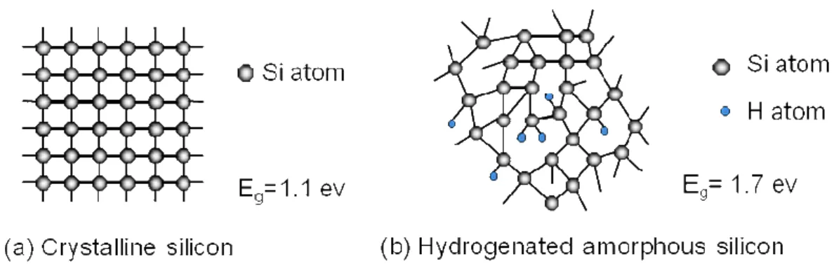
Figure 1.3 illustrates the different silicon network in crystalline silicon and hydrogenated
amorphous silicon. Crystalline silicon is a four-fold coordinated atom that is normally
tetrahedrally bonded to four neighboring silicon atoms. The tetrahedral structure is continued
over a large range, forming a well-ordered lattice (crystal), as shown in Figure 1.3 (a).
Hydrogenated amorphous silicon (a-Si:H) is the non-crystalline allotropic form of silicon.
It can be deposited in thin films at low temperatures onto a variety of substrates. In
amorphous silicon this long range order is not present and the atoms form a continuous
random network, as shown in Figure 1.3 (b). Although amorphous silicon lacks the long range
order, it has the same short range as single crystalline silicon. Due to the disordered nature of
the amorphous silicon, some silicon atoms have a dangling bond. There are covalently bonded
to only three silicon atoms and have on unpaired electron, a so-called dangling bond. These
dangling bonds are defects in the silicon random network, which cause anomalous electrical
behavior.
When amorphous silicon was deposited in such a way that hydrogen can be incorporated
in the atomic network, the material can be passivated by hydrogen. Thus, the dangling bond
density can reduce by several orders of magnitude. In general, there exist about 10 at.%
hydrogen concentrations in hydrogenated amorphous silicon thin film. Because hydrogen
radical would passivate dangling bond, hydrogenated amorphous silicon has a sufficiently low
amount of defects to be used within devices. Due to Si-H bonding (1.7eV) was formed,
amorphous silicon bandgap (1.75eV) is large than crystalline silicon bandgap (1.12eV).
However, the hydrogen is unfortunately associated with light induced degradation of the
material, termed the Staebler-Wronski effect.
One advantage is that a-Si or its alloys can be deposited at very low temperatures. This
allows for deposition on not only glass, but plastic as well, making it a candidate for a
roll-to-roll processing technique [4-6]. Another advantage is that amorphous silicon can be
deposited over large areas by PECVD.
1.3 The Structure of Thin Film Solar Cell
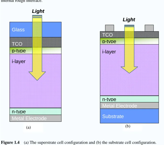
There are two basic configurations of thin film solar cell, as shown in Figure 1.4. From
the Figure 1.4(a), it is termed superstrate configuration and the substrate usually is used
transparent material. The p-layer is deposited first, then the intrinsic layer and the n-layer
deposited last. From the Figure 1.4(b), it is substrate configuration and occurs when a cell is
configuration. In the case of the superstrate configuration, the glass usually was coated with
transparent conductive oxide (TCO) film. In addition, the TCO layer has to be surface
textured in order to enhance light absorption inside the solar cell due to the scattering at
internal rough interface.
Figure 1.4 (a) The superstrate cell configuration and (b) the substrate cell configuration.
Thin film a-Si:H must be grown with an intrinsic region as opposed to pn junction to
compensate for low carrier drift mobility. The electric field across the intrinsic region is
required to achieve effective separation of generated carriers and a rectifying junction. (b)
i-layer
n-type
Metal Electrode
p-type
TCO
Glass
i-layer
n-type
Metal Electrode
p-type
TCO
Substrate
L
L
i
i
g
g
h
h
t
t
L
L
i
i
g
g
h
h
t
t
(a)Both configurations are usually illuminated through a TCO/p-layer interface. This
improves cell performance by generating most carriers close to this interface, lowing hole
recombination probability. Due to the low hole mobility of a-Si:H, efficient collection is a
priority for ensuring good cell performance. So the p-layer also call window layer in the solar
cell structure.
1.4 AM1.5 Light Source
Solar radiation closely matches a black body radiator at 5,800 K. As the sunlight travels
though the atmosphere, chemicals react with the sunlight and absorb certain wavelengths.
Perhaps the best known example is the stripping of ultraviolet light by ozone in the upper
atmosphere, which dramatically reduces the amount of short wavelength light reaching the
Earth's surface. A more active component of this process is water vapor, which results in a
wide variety of absorption bands at many wavelengths, while molecular nitrogen, oxygen and
carbon dioxide add to this process.
Atmospheric scattering also plays a role, removing higher frequencies from direct
sunlight and scattering it about the sky. The greater the distance of atmosphere the sunlight
travels through, the greater this effect, which is why the sky looks pink at sundown when the
For a thickness lo of the atmosphere, the path length l through the atmosphere for solar
radiation incident at angle θ relative to the normal to the Earth's surface is
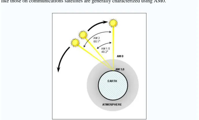
l = lo / cos θ (1) The ratio l / lo is the air mass coefficient.
As shown in Figure 1.5, the spectrum outside the atmosphere, the 5,800 K black body, is
referred to as "AM0", meaning "zero atmospheres". Cells used for space power applications,
like those on communications satellites are generally characterized using AM0.
Figure 1.5 Schematic of air mass
The spectrum after traveling through the atmosphere to sea level with the sun directly
overhead is referred to as "AM1". This means "one atmosphere". Conveniently, silicon solar
cell development is concentrated in the United States, Europe and Japan, an AM number
representing the spectrum at mid-latitudes is much more common. "AM1.5", which is
1.5 times the atmosphere thicknesses, corresponds to a solar zenith angle of 48°, and is almost
universally used to characterize solar panels. "AM1.5G", where G stands for ‘global’ and
includes both direct and diffuse radiation.
1.5 Staebler–Wronski Effect
The Staebler-Wronski Effect (SWE) refers to light-induced metastable changes in the
properties of hydrogenated amorphous silicon. The defect density of hydrogenated amorphous
silicon (a-Si:H) increases with light exposure, to cause an increase in the recombination
current and lead to the reduction in the sunlight to electricity conversion efficiency. It was
discovered by Staebler and Wronski in 1977 [3]. They showed that the photo-conductivity of
hydrogenated amorphous silicon can be reduced significantly by prolonged illumination with
intense light. However, it could reverse the effect by heating the samples to above 150℃.
The efficiency of an amorphous silicon solar cell typically drops during the first six
months of operation. This drop may be in the range from 10% up to 30% depending on the
material quality and device design. After this initial drop, the effect reaches equilibrium and
causes little further degradation. Most commercially available a-Si modules have SWE
degradation in the 10 to 15% range and suppliers typically specify efficiency based on
cell the efficiency is reduced by up to 30% in the first 6 months as a result of the
Staebler–Wronski effect, and the fill factor falls from over 0.7 to about 0.6. This light induced
degradation is the major disadvantage of amorphous silicon as a photovoltaic material.
1.6 PECVD
Plasma enhanced chemical vapor deposition (PECVD) system is widely used to fabricate
silicon thin film solar cell. Using PECVD system to deposit silicon thin film is a low
temperature process, usually less than 300℃. So silicon thin film can deposit onto variety of
substrates such as glass, stainless steel, or plastic substrate. Comparing the silicon wafer
substrate, employing the above substrates is the good point of view to industry for large scale
productions and cost drop. Besides, doping and alloy layers are made easily by using PECVD
method. For example, introducing source gases SiH4 and B2H6 or SiH4 and PH3 mixture,
doping layers can be easily deposited onto different substrates.
1.7 An Overview of Amorphous Silicon Solar Cell
First commercially available thin-film solar cells based on a-Si:H were produced for
consumer applications such as pocket calculators and solar watches. Today, a new generation
of a-Si:H-based solar modules enters the market focusing on power applications. Several
manufacturing facilities with multi-megawatt capacity have started production, are currently
being installed, or are announced [4, 7, 8].
in 1976 [9]. This single junction p-i-n a-Si:H solar cell deposited on a glass substrate coated
with transparent conductive oxide (TCO) and aluminium back contact exhibited a 2.4%
conversion efficiency. Only one year later Staebler and Wronski discovered the light-induced
degradation of a-Si:H (Staebler–Wronski effect, SWE) [3]– a severe drawback in a-Si:H solar
cell technology. During exposure of solar cells to light the SWE results in a decrease of
efficiency until a saturation value is reached. Since the recognition of the SWE, development
strategies have focused on improvements of the stabilized efficiency reached after long-term
operation. The stacked-cell concept has emerged as a powerful tool to enhance the stabilized
efficiency [10]. Moreover, the use of component cells with different optical bandgaps
provides a better utilisation of the solar spectrum [11, 12].
Much research in the field of a-Si:H solar cell was devoted to developing and
optimizing a-Si:H base alloys in the 1980s. A p type hydrogenated amorphous silicon carbide
(a-SiC:H) was incorporated in solar cells as a low absorbing layer, usually denoted as a
window layer [13]. Hydrogenated amorphous silicon germianium (a-SiGe:H) became an
attractive low bandgap material for stacked solar cells [14]. Surface textured substrates were
introduced to enhance optical absorption [15]. Optimized transparent conductive oxide (TCO)
films and TCO/metal back reflectors minimize reflection losses and provide an effective light
trapping.
a-SiGe:H (hydrogenated amorphous silicon germanium) films and corresponding alloys
improves the electronic properties of these materials in both the initial and the light-soaked
state [16–18]. All these techniques are combined in a triple-junction a-Si/a-SiGe:H/a-SiGe:H
cell which yields a stable active area efficiency of 13% [12]. This value represents the current
world record for solar cells based on a-Si:H and its alloys. Hydrogenated microcrystalline
silicon deposited by the low temperature PECVD technique emerged in this period as a new
candidate for the low bandgap material in multijunction a-Si:H based solar cells [19].
Research has concentrated on understanding and improving light trapping
techniques, where surface textures as well as new TCO material play a crucial role. This
activity has resulted in the commercialization of novel deposition techniques for ZnO as an
alternative TCO material for SnO2 [20]. Several deposition machine manufacturers have
started developing commercial production machines for the fabrication of thin film silicon
solar cell [21]. Most improvements in stabilized solar cell efficiency are based on adapted cell
designs and advanced light-trapping concepts. Many fundamental questions remained
regarding the growth and the material properties of a-Si:H and its alloys as well as the optical
and electrical function of complete solar cell devices.
1.8 Motivation
Thin film silicon in general, are expected to be promising material for applications to
device-grade a-Si:H, reactive sputtering, mercury-sensitized photo-chemical-vapor deposition
(CVD), direct-photo CVD, hot-wire CVD, and plasma-enhanced CVD (PECVD). Among the
variety of growth methods, PECVD is widely used due to its high potential for yielding a
uniform high-quality silicon thin film on a large-area substrate.
In this study, hydrogenated amorphous silicon (s-Si:H) solar cell was fabricated by
Radio-Frequency Plasma Enhanced Chemical Vapor Deposition (PECVD). The absorption in
the a-Si:H intrinsic layer contributes to the current generation, the optimal optical and
optoelectronic property was crucial role for solar cell performance. Due to lower mobility of
holes in comparison to electrons in a-Si:H , the p-layer a-Si:H of quality is the other effect for
solar cell performance. Because light enters the solar cell through the p-layer, there is
substantial absorption in this layer. The photogenerated carriers in the p-layer do not
contribute to the photocurrent because the electron quickly recombined. Therefore, the
absorption of the p-layer has to minimize, which is done by minimizing the thickness and
alloying the p-layer with carbon.
1.9 Thesis Outline
This thesis is organized into the following chapters:
In the chapter 1, a brief overview of thin film solar cell technology is introduced to
describe its advantages and bottlenecks. The motivation of the studies is also described in
In the chapter 2, the process flow of the samples is introduced. The measurement method
also shows here in detail.
In the chapter 3, here shows the dependence of material properties and device
performance on various conditions with different hydrogen dilution ratios.
In the chapter 4, this chapter will discuss the results from chapter 3. The effect and the
dependence of the material properties on different conditions will be explain here.
In the chapter 5, the results of our experiments in chapter 3 and discussions in chapter 4
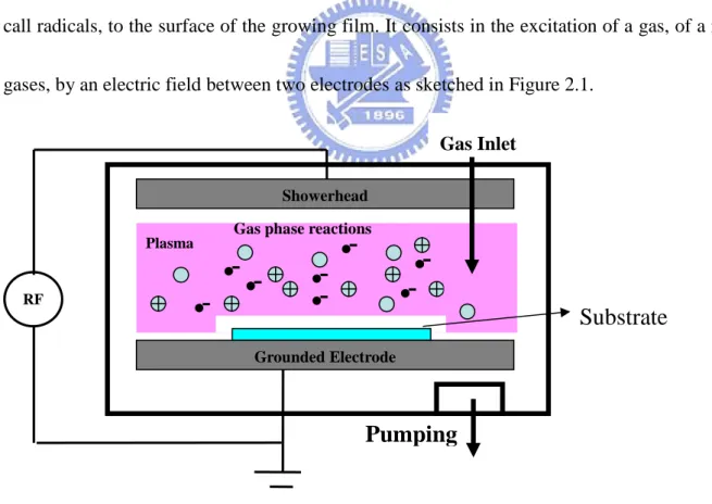
Chapter 2 Experimental Details
2.1 Radio-Frequency Plasma-Enhanced Chemical Vapor DepositionPlasma-enhanced chemical vapor deposition (PECVD) is common technique used
during the manufacturing of most microeletronic device. The role of the plasma is to provide
a source of energy to dissociate silicon bearing gas, which is usually silane (SiH4), hydrogen
(H2), etc. This is done by collisions with electrons, which originate as secondary electrons in
the plasma an build up their energy by acceleration in an electric field. The growth of an
a-Si:H film is accomplished by attaching reactive particles of dissociated silane molecules,
call radicals, to the surface of the growing film. It consists in the excitation of a gas, of a mix
gases, by an electric field between two electrodes as sketched in Figure 2.1.
Figure 2.1 Schematic diagram of capacitively-coupled rf PECVD system
RF
Pumping
Plasma
Substrate
Grounded Electrode Gas phase reactions
Showerhead
The initial event in the growth process of a-Si:H is electron-impact dissociation of
the source gas materials in silane (SiH4) and silane-to-hydrogen (SiH4/H2) glow-discharge
plasma. SiH4 and H2 molecules were through electronic excited states of these molecules by
inelastic collisions with high-energy electros in the plasma. Electronic excited states of
complicated molecules such as SiH4 are usually dissociating states at which dissociation
occurs spontaneously to SiH3, SiH2, SiH, Si, H2 and H.
Reactive neutral and ionic species produced in the plasma undergo secondary
reaction mostly with SiH4 and H2 molecules, forming a steady state. Rate constants for each
reaction are summarized in the literature [22]. Therefore, highly reactive species such as SiH2,
SiH, and Si (short-lifetime species) have much smaller values of densities than SiH3 in the
steady-state plasma, although the generation rates of those species are not very different from
that of SiH3, which indicates low reactivity with SiH4 and H2( long-lifetime species).
In the growing amorphous silicon, the SiH3 radicals reaching the film-growing
surface start to diffuse on the surface. During surface diffusion, SiH3 abstracts
surface-covering bonded hydrogen, forming SiH4 and leaving a dangling bond on the surface
(growth-site formation). Another SiH3 radical toward the dangling-bond site on the surface
and forms the Si-Si bond (film growth), as schematically shown in Figure 2.2. This surface
reaction scheme for film growth has been proposed on the basis of two experimental results
Figure 2.2 Surface reactions during the a-Si:H film growth [23]
Through other radicals contribute much less to the growth, they do play an important
role in determining the properties of the film. The SiH2 and higher silane radicals have higher
sticking coefficients than SiH3 and be incorporated directly into the hydrogen terminated
surface [24]. However, the contribution of these radical to the growth results in poor quality
film, and therefore the presence of these radicals in the plasma should to be avoided.
An important advantage of plasma enhanced CVD deposition is that the deposition is
2.2 Introduction of Experiment
Hydrogenated amorphous silicon films were deposited using pure SiH4 by radio
frequency (27.12 MHz) plasma enhanced chemical vapor deposition (PECVD) system.
Doping layers were prepared by using B2H6 or PH3 with pure SiH4 and H2 dilution.
Amorphous silicon carbide was deposited by mixing SiH4 and CH4. Prior to deposit all the
samples, the chamber was introduced gas NF3 and Ar to clean the chamber. Corning
Eagle2000 glass and crystalline silicon wafer substrate were clean by KG Cleaner and RCA
standard cleaning process, respectively. All the samples were started to prepare after the
background pressure of the reactor chamber reach to 10-7 torr. In this study, samples were
prepared simultaneously on 5.0 cm * 5.0 cm Corning Eagle 2000 glass and 1.5cm * 1.5cm
c-si wafer. The samples gown on glass substrate was used to analysis optoelectrial properties
and the films on c-si wafer were used to determine the hydrogen bonding configuration. The
devices were deposited on the glass coated TCO.
The complete range of deposition conditions include: substrate temperature (TS) :
190~210°C, pressure: 0.3~1 torr, background pressure: 10-7 torr, power: 20~40 W, electrode
2.3 Determination of Thin Film Thickness
The measurement of thin film thickness has a lot of methods such aAlpha stepper and
ellipsometery. In the measurement of the alpha stepper, it has to be step profile. So chemical
etching is necessary to make step high. Chemical etching may occur by any of several
different processes. The simplest modes of etching involve dissolution of the material in a
liquid solvent without any change in the chemical nature of the dissolved species. So
choosing solvent is important for chemical etching. And we find the material, 30 wt.% KOH,
can etch silicon. Although it still etches silicon dioxide, it etches slowly at room temperature.
Figure 2.3 The dependence of etching rate of the [100] silicon in 30 wt.% KOH on temperature [25]
Figure 2.4 The dependence of etching rate of the silicon dioxide in 30 wt.% KOH on temperature[25]
The Figure 2.3 and Figure 2.4 show the correction between the etching rate and
temperature[25]. The 30 wt.% KOH can etch amorphous silicon. We use the tape attach a part
of sample area. It immerses in the 30 wt.% KOH, until the amorphous silicon was removed.
This method leaves a well defined step profile which was measured at intervals of 25mm
along the length of the slide using a mechanical alpha step.
2.4 Conductivity Analysis
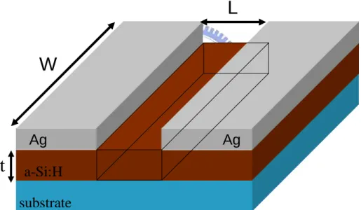
In order to investigate the conductivity of the a-Si:H, metal contacts were deposited by
thermal evaporation method onto the film. Conductivity (σ) is calculated by equation (2),
to conductivity is determined by the width (W), length (L), and thickness (t) of a cuboid
located between the conducting contacts used to probe the sample in the Figure 2.5.
(2)
A prepared a-Si:H film with silver contacts is show in Figure 2.5. Photo-conductivity
was measured by AM1.5G light spectrum with power at 100mw/cm2. For the amorphous
silicon germanium film, the thickness is about 600 nm. For the intrinsic amorphous silicon,
the thickness is about 600 nm. The thickness of doping layer is about 200 nm .
Figure 2.5 Sample configuration for the conductivity measurement of a-Si:H, where t is the film thickness
2.5 Determination of Optical Properties
2.5.1 Tauc Bandgap
The optical bandgap of thin film use UV/VIS/NIR spectrometers to measure
substrate
a-Si:H
Ag
W
t
Ag
L
=
t
1
W
L
V
I
σ
transmission (T) spectra were carried out between 200nm and 1.3 µm in the step of 2 nm.
Calculating optical bandgap (Eg) has to use transmission spectra and thickness of thin film in
equation (3).
(
α
h
ω
)
2=
c
(
h
ω
−
E
opt)
1
(3)
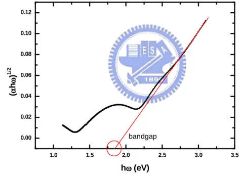
Where α is the absorption coefficient of a-Si:H,
h
ω
is the photon energy, and Eopt is Taucoptical bandgap. From Figure 2.6,
(
α
hω
)
12as a function of the photo energy( )
h
ω
. Thebandgap value can be determined from the expanding linear region line intercepts a-axis.
1.0 1.5 2.0 2.5 3.0 3.5 0.00 0.02 0.04 0.06 0.08 0.10 0.12 (αααα hωωωω ) 1 /2 hωωωω (eV) bandgap
Figure 2.6
(
α
hω
)
12 as a function of photon energy( )
hω
, and the Tauc bandgap2.5.2 Fourier Transform Infrared Spectroscopy
Since hydrogen is an important element in passivation, the incorporation and stability of
hydrogen in a-Si:H has the topic of intensive research. Infrared absorption spectroscopy is
Three characteristic infrared absorption bands are observed in a-Si:H: a peak at 640 cm-1, and
absorption peaks in the rage of 2000-2200cm-1. The peak at 640 cm-1 reflects the rocking
mode of hydrogen covalently bonded in all possible bonding configurations, such as silicon
monohydride (SiH), dihydride (SiH2), and trihydride (SiH3) and polymeric (Si-H2)n bonding
configurations. Thus, this peak is used to determine the hydrogen content in a-Si:H [26]. And
peak around 2000cm-1 isassigned to the stretching mode of the isolated Si-H bonds and a peak
in the range of 2060-2160cm-1 includes contributions from the stretching mode of Si-H bonds
at internal surface, such as voids, Si-H2 and Si-H3.
Infrared absorption measurements were made with Fourier Transform Infrared
Spectroscopy on films deposited on crystalline silicon. The data were analyzed following
Brodksy et al. [27]. The integrated absorption, I, for each bond was determined from the
relationship.
( )
d
I
ω
ω
ω
α
∫
=
(4)Where α(ω) is the absorption coefficient of the film at the wavenumber ω. A ‘microstructure
parameter’, denoted as R, is determined from the equation (5).
SiH2 SiH SiH2
I
I
I
R
+
=
(5)Where ISiH and ISiH2 are the integrated absorption strength of the peak at wavenumber
integration of the Si-H rocking-wagging mode [28] at 640 cm-1. The complete procedure can
be expressed by the following equation (6):
(
)
=
∫
∞∞( )
≈
∑
( )
∆
N
A
d
N
A
at.%
C
-si w si w Hω
ω
ω
α
ω
ω
ω
α
(6)Where Aw=1.6x1019 cm-2 is the proportionality constant, and Nsi=5x1022 cm-3 is the
atomic density of pure silicon.
2.6 Measurement of Thin Film Solar Cell
An I-V characteristic is measured by performing a voltage sweep from a small reverse
of forward bias whilst measuring current flow at each bias point. An illuminated I-V
characteristic provides a figure for cell efficiency and incident light source is AM 1.5G with
power density 100mW/cm2. Isc and Voc can be determined directly from the vertical and
horizontal intercepts of the sweep.
From Figure 2.7, it shows a typical illuminated I-V characteristic using real measured
data. The current density is that measured current divided by cell area. The corresponding
power function is shown alongside it and this is created by multiplying every voltage bias
point of the I-V characteristic by the current measured at that bias. Important labeled features
of the graphs include Voc, Jsc, the bottom of the graph is maximum power density
Figure 2.7 (a) The I-V characteristics and (b) power density versus voltage of solar cell, Vm and Im are the voltage and current corresponding to the maximum power density of the cell
The solar cell efficiency (η) is the ratio between incident light power density (Pin) and
the device convert the maximum power density. Equation (7) can calculate the cell efficiency.
P
I
V
P
P
in m m in Max=
=
η
(7) (a) -0.4 -0.2 0.0 0.2 0.4 0.6 0.8 1.0 -10 -5 0 5 10 15 20 C u rr e n t D e n s it y ( m A /c m 2 ) Voltage(V)V
ocJ
scP
max(V
m, J
m)
-0.4 -0.2 0.0 0.2 0.4 0.6 0.8 1.0 -10 -5 0 5 10 15 Voltage(V) P o w e r D e n s it y (m W /c m 2 )P
max(V
m,J
m)
(b)Where the ratio of the maximum power density (PMax = Vm Jm) and Pin is the light source
power density. And the other parameter is the fill factor (FF) can describe PV solar cell quality.
It is the ratio of the maximum power density (PMax = Vm Jm) and a cell should supply if it was
ideal (P = Voc Jsc) like equation (8). And the FF can be connect with the efficiency, it like the
equation (9). sc oc Max
J
V
P
FF
=
(8) in sc oc in m mP
FF
J
V
P
I
V
=
=
η
(9)Chapter 3 Result and Discussion
3.1 Optimization of Intrinsic Hydrogenated Amorphous Silicon3.1.1
Effect of the Silane Flow Rate on the Film Property
The optoelectronic properties of the a-Si:H deposited by the PECVD are dominated by
deposition parameters , such as pressure of the gas, flow rate , substrate temperature , power
density, the electrode spacing, etc. In this work, we discuss the effects of the silane flow rate
and electrode distance on the qualities of amorphous silicon thin films.
Here, the substrate temperature was held at 190℃. As shown in Figure 3.1, the dark-
conductivity (σdark) and photo-conductivity (σphoto) as a function of the silane flow rate are
demonstrated. 20 40 60 80 10-12 10-11 10-10 10-9 10-8 10-7 10-6 10-5
σσσσ
dark C o n d u c ti v it y ( c m −1−1−1−1 ΩΩΩΩ −1−1−1−1 ) SiH 4 Flow (sccm)σσσσ
PhotoFigure 3.1 The dark-conductivity (σdark) and the photo-conductivity (σphoto) as a function of
From Figure 3.2, the dependence of deposition rate with on silane flow is also illustrated.
The deposition rate significantly increased with raising silane flow rate from 15 to 30 sccm.
When silane flow rate was raised from 30sccm to 80 sccm, the deposition rate didn’t change
too much. The surface reaction caused the restriction of deposition rate. Both the σphoto and
σdark decreased with increasing of the silane flow rate.
20 40 60 80 2.5 3.0 3.5 4.0 D e p o s it io n r a te ( A /s ) SiH 4 Flow (sccm) Figure 3.2 The dependence of deposition rate on silane flow rate
The dependence of hydrogen bonding configuration on silane flow rate is illustrated in
the Figure 3.3. The integrated absorption of SiH and SiH2 species depended on the silane flow
rate, as shown in Figure 3.4. The hydrogen content almost was constant. When the silane flow
rate varied from 30sccm to 50sccm, the R value was minimized. The silane was depleted
20 40 60 80 0.0 0.2
R
SiH
4Flow (sccm)
6 8 10 12H
c
o
n
te
n
t
(a
t.
%
)
Figure 3.3 The microstructure parameters and the hydrogen content as a function of the silane flow rate
0 20 40 60 80 10 20 30
SiH
4Flow (sccm)
In
te
g
ra
te
d
A
b
s
o
rp
ti
o
n
(
a
rb
.u
n
it
)
SiH (2000cm
-1)
SiH
2(2090cm
-1)
Figure 3.4 The integrated absorption of the SiH and SiH2 bonding configurations as a
On the contrary, the silane flow rate was so much that induced gas phase reaction
drastically. The SiH2 bonding increased slowly as silane flow rate from 50sccm to 80 sccm.
The good qualities of amorphous silicon thin films were attained while the silane flow rate
varied from 30 sccm to 50 sccm. The films contained a majority of SiH2 bonding while the
silane entirely decomposed, which was in agreement with the study of Knights and Lujan [29]
and Street et al. [30].
3.1.2 Effect of the Electrode Spacing on the Film Property
The photo- and dark-conductivity of intrinsic a-Si:H was depended on electron spacing,
as shown in the Figure 3.5. The dark-conductivity decreased with increasing electrode
spacing. 16 20 24 10-11 10-10 10-9 10-8 10-7 10-6 10-5
σσσσ
darkElectrode Spacing (mm)
C
o
n
d
u
c
ti
v
iy
( ΩΩΩΩ -1
c
m
-1 )σσσσ
PhotoFigure 3.5 Dependence of photo- (σphoto) and dark-conductivity (σdark) of intrinsic a-Si:H on
Due to the property of defect would cause the film to be more conductive or resistive,
the quality of films didn’t determine by the dark-conductivity. From the Figure 3.6, deposition
rate significantly increased as raising electrode spacing. Increasing electrode spacing induced
more gas-phase reaction. That is reason the deposition rate increase strongly when the
electron spacing varied from 20mm to 25mm.
16
20
24
1
2
3
4
5
6
D e p o s it io n R a te ( A /s ) Electrode Spacing (mm)Figure 3.6 The deposition rate as a function of the electrode spacing
The results of IR spectra were shown in the Figure 3.7, including the hydrogen content
and microstructure parameters with different electrode spacing, respectively. From
the Figure 3.8, the hydrogen bond configuration of SiH and SiH2 bonding was as a function of
16 20 24 0.0 0.2 0.4 R Electrode Spacing (mm) 6 8 10 12 H C o n te n t (a t. % )
Figure 3.7 The hydrogen content and microstructure parameters versus the electrode distance, respectively 12 16 20 24 0 10 20 30 Electrode Spacing (mm) In te g ra te d A b s o rp ti o n ( a rb .u n it )
SiH
2(2090cm
-1)
SiH (2000cm
-1)
Figure 3.8 The integrated absorption of the SiH and SiH2 bonding configurations versus the
It figured out that the increases of microstructure and hydrogen content were due to
increase electrode spacing. The electrode spacing significantly affected on SiH and SiH2
species contained in the film. When the electrode distance increased, it caused more gas-phase
reaction. Therefore, it induced the increase of SiH2 bonding. It concluded the optimal
electrode spacing of film quality was in the range of from 14mm to 17mm.
The different hydrogen bonding configuration within the film can be understood from
Paschen’s law. Increasing pressure or electrode spacing, the electrons are more likely to
collide with the plasma constituents than the electrodes. Thus, it promotes polymerization and
can lead to the inclusion of SiH2 chain within the film. On the other hand, as pressure is
lowered or as electrode spacing is decreased, the electron energy is limit by collision with the
electrodes. In this study, it concluded that increasing electrode spacing induces more
gas-phase reaction.
3.2 Doping of Hydrogenated Amorphous Silicon
3.2.1 Phosphorus Doping of n-type a-Si:H
The purpose of doping is to change electrical conductivity and its magnitude by adding
a controlled amount of impurity atoms. The principal doping elements used in a-Si:H are the
same as in crystalline silicon, boron for p-type and phosphorus for n-type material. It change
conductivity of a-Si:H by mixing the silicon source gas, silane (SiH4), with phosphine (PH3)
2 4
10-3
10-2
10-1
PH3/SiH4 Flow Ratio (x10-3)
D a rk C o n d u c ti v it y ( ΩΩΩΩ −1−1−1−1 c m -1 )
Figure 3.9 Dark-conductivity as function of the phosphine-to-silane flow ratio
2 4
2 4
PH3/SiH4 Flow Ratio (x10-3)
D e p o s it io n r a te (A /s ) 1.0 1.5 2.0 2.5 B a n d g a p (e v )
Figure 3.10 The bandgap and deposition rate as function of the silane-to-phosphine flow ratio
From the Figure 3.9, the dark-conductivity as a function of the diborane-to-silane flow
ratio. As a result of heavy doping, the dark-conductivity didn’t change too much. The
dark-conductivity was almost 10-2 (Ω-1Cm-1). As shown in the Figure 3.10, the bandgap and
deposition rate as a function of phosphine-to-silane flow ratio. The doping material was too
small concentration to change the bandgap.
3.2.2 Boron Doping of p-type a-Si:H
The dark-conductivity (σd) of p-type a-Si:H as a function of the diborane-to-silane flow
ratio, as shown in the Figure 3.11. The conductivity increased as increasing flow ratio.
But the diborane-to-silane flow ratio was large than 1, the conductivity didn’t increase.
Because the doping of a-Si:H inevitably caused the creation of dangling bond [32], it reduced
the conductivity. 0 1 2 10-6 10-5 10-4 D a rk C o n d u c ti v it y ( ΩΩΩΩ -1 c m -1 ) B
2H6/SiH4 Flow Ratio (x10
-2 )
An additional important different between a-Si:H and single crystal silicon is that when
the concentration of boron and phosphorous atoms in a-Si:H increase, then Fermi level
doesn’t move close to the valence and conduction band mobility edges than 0.3eV and to
0.15eV, respectively. 0 1 2 2 4 D e p o s it io n R a te (A /s ) 1 2 B
2H6/SiH4 Flow Ratio (x10 -2 ) B a n d G a p (e v )
Figure 3.12 Bandgap and deposition rate versus the diborane-to-silane flow ratio
The presence of tail and defect states in the bandgap does not allow a full shift of the
Fermi level towards the band edges. This is the reason the conductivity of p-type amorphous
silicon was lower than n-type.
3.3 Optimization of Hydrogenated Amorphous Silicon Carbide
The purpose of alloying a-Si:H for photovoltaic application is to shift the optical
absorption spectrum to higher of lower photon energies and in this way to adjust the optical
slightly changed by varying the hydrogen content in a film [33]. This is done by changing the
deposition conditions, such as the substrate temperature of dilution of silane with hydrogen. A
substantial shift of the absorption coefficient can be achieved by alloying a-Si:H with carbon,
oxygen, nitrogen or germanium.
1.0 1.5 2.0
10-6 10-5 10-4
CH4/SiH4 Flow Ratio
C o n d u c ti v it y ( ΩΩΩΩ −1−1−1−1 c m -1 )
Figure 3.13 The conductivity of a-SiC:H versus the methane-to-silane flow ratio
Alloying can easily be accomplished by adding the appropriate gases to the silane
source gas in the CVD process. Amorphous silicon carbide is mixed silane with methane in
the process. It can easily change the amorphous silicon bandgap by varying the methane-to-
silane flow rate ratio[34, 35]. The conductivity and bandgap depended on methane-to-silane
flow ratio, as shown in the Figure 3.13. The conductivity of doped a-SiC:H decreased strongly,
more by alloying carbon. 1.0 1.5 2.0 2 4 D e p o s it io n R a te (A /s ) CH
4/SiH4 Flow Ratio
1.8 2.0 B a n d G a p (e v )
Figure 3.14 The bandgap and deposition rate as a function of the methane-to-silane flow ratio
The bandgap verses methane-to-silane flow ratio as shown in the Figure 3.14.
The effective of alloying carbide can improve bandgap for amorphous silicon.
The bandgap of the p-type amorphous silicon typical is 1.7 eV, but the amorphous silicon
carbide was large than 2 eV. Therefore, amorphous silicon carbide can improve the device
performance by inducing more photo energy to the device. On the other hand, alloying carbon
would reduce the conductivity. Thus, The p-layer a-SiC:H is a trade-off between conductivity
3.4 Hydrogenated Amorphous Silicon Solar Cell
3.4.1 Solar Cell Fabrication on TCO-Coated Glass
In a-Si:H, the diffusion length of the charge carriers is shorter than in crystalline silicon.
In intrinsic a-Si:H, the ambipolar diffusion length is about 0.1 to 0.3 µm. In doped a-Si:H layers,
the defect density of doping a-Si:H is two or three orders of magnitude higher than intrinsic
a-Si:H. Due to the short diffusion length the photogenerated carriers would virtually all
recombine in the doped a-Si:H layers before reaching the depletion region of the p-n junction.
Therefore, an a-Si:H solar cell is designed differently compared to the standard p-n junction of
a crystalline silicon solar cell.
The doped layer are usually very thin at a-Si:H thin film solar cell. The thickness of
p-type a-SiC:H layer is less than 30nm thick, the thickness of the a-Si:H p-layer is less than
30nm thick, and an n-type a-Si:H is less than 30nm thick. The doping layer has two function of
the amorphous silicon solar cell. First, a sufficiently high electrical conductivity is required for
both p- and n- layers in order to form a high built-in voltage across the p-i-n junction. Second,
the doping layers establish low loss ohmic electrical contact with the electrode. The
steabler-Wronski effect deteriorate the collection of carriers, the thickness of intrinsic
amorphous silicon can’t be too thick. So the optimal thickness of the thickness of the intrinsic
layer is in the range of 250nm to 320 nm [36]. The deposition conditions of each layer in the
p-layer (a-Si:H) p-layer (p-a-SiC:H) i-layer (i-a-Si:H) n-layer (n-a-Si:H) Substrate temperature (℃℃℃) ℃ 190 190 190 190 Deposited
material SiH4+B2H6 SiH4+CH4+B2H6 SiH4 SiH4+PH3+H2
Table 3.1 The deposition condition of each layer in the fabricated a-Si:H solar cell
-0.5 0.0 0.5 1.0 1.5 -10 0 10 20
a-SiC:H
p-layer
C u rr e n t D e n s it y (m A /c m 2 ) Voltage (V)a-Si:H
p-layer
As-deposited
Figure 3.15 Photovoltaic performance of the as-deposited solar cell with a-Si:H and a-SiC:H as window layers
From the Figure 3.15, photovoltaic performances of the as-deposited solar cell with
a-Si:H p-layer and a-SiC:H p-layer, respectively. The characteristic of solar cell with different
shows increase in the open-circuit voltage (Voc) from 0.75V to 0.78V and in the short–circuit
current (Jsc) from 10.23 mA/cm2 to 12.76 mA/cm2 at the same time. Because the wide bandgap
p-layer also increases the open-circuit voltage by reducing recombination at the p-i interface
[37]. p-layer
V
oc(V)J
sc(mA/cm2)FF
(%)η
(%) a-Si:H (1.75eV) 0.752 10.23 65 5 a-SiC:H (1.94eV) 0.788 12.76 64.12 6.57Table 3.2 The solar cell parameters with different p-layer material
But in the I-V curve shows an S-shaped character, which the current starts falling off
already at low forward bias.The curve bending in the Figure 3.15 has shown an imperfection of
the cell. Therefore we performed a thermal annealing process try to eliminate the current
instability and enhance the performance of the solar cell.
3.4.2 Effect of Annealing on cell Performance
In the Figure 3.15 shows an S-shaped character, which the current starts to fall off already
at low forward bias. In order to find the origin for this S-shaped I-V characteristic, the
photovoltaic property of a pin type solar cell is characterized by the series resistance Rs and the
performance. The bias-annealing increased the open-circuit voltage, fill factor, and the cell
efficiency [38]. Their conclusion is the series resistance and the shunt resistance of the
hydrogenated amorphous silicon solar cell can be observed to decrease and increase
respectively after bias-annealing [39].
-0.5 0.0 0.5 1.0 1.5 -10 0 10 As-deposited 75oC anneal 100oC anneal 150oC anneal 210oC anneal C u rr e n t D e n s it y (m A /c m 2 ) Voltage (V)
AM1.5 Cell Area=0.25cm2
150oC
Figure 3.16 The I-V curves for the as-deposited, and the annealed solar cell after annealing at 75℃, 100℃, 150℃ 210℃, respectively ,
The important parameter is annealing temperature. Y. Arai et al. eliminated the process of
bias-annealing. They also can improve solar cell performance by annealing without bias [40].
Figure 3.16 shows the I-V curve for the as-deposited, and the annealed solar cell after annealing
temperature at 75℃, 100℃, 150℃, 210℃, respectively. The result shows that with adequate
Figure 3.17. The results in the Figure 3.17 indicate significant increase of Voc and FF, while Jsc
remains the same.
0 50 100 150 200 250 0.7 0.8 0.9 Annealing Temperature(oC) V o c (v ) 12 14 J sc (m A /c m 2 ) 60 75 F F ( % ) 6 8 10 ηηηη ( % )
Figure 3.17 Voc, Jsc, fill factor and efficiency of the solar cell as a function of the annealing
temperature
In the thin film silicon solar cell, there are three main factors can affect the fill factor.
First, the recombination loss in the i-layer or at the p/i and n/i interface. Second, partial
micro-shunts through the i-layer. Third, the contact and doped layers are too high resistance
which may due to the degradation of interface quality.
In order to investigate the thermal annealing effect for the solar cell, experiment of the
sequence between Ag deposition and annealing was carried out Ag deposition and annealing
was carried out. The IV curve of the solar cell which were annealed before and the Ag
electrode was deposited, as compared to the as-deposited cell, as shown in the Figure 3.18.
The result indicates that the n/Ag interface and contact quality is main issue for the thermal
annealing. The as-deposited and the annealing without Ag electrode didn’t change observably.
But the annealing after Ag electrode deposited improved performance with annealing 150 ℃.
-0.5 0.0 0.5 1.0 1.5 -10 -5 0 5 10 15 20
C
u
rr
e
n
t
D
e
n
s
it
y
(m
A
/c
m
2)
Voltage (V)
As-depositedAnneal before Ag deposited Anneal after Ag deposited
Annealing Temprature = 150
oC
Figure 3.18 The I-V curves of the solar cells which were annealed before and after the Ag electrode was deposition, as compared to the as-deposited cell
Voc(V) Jsc (mA/Cm2) FF (%)
ηηηη(%) As-deposited 0.788 13.11 65.32 6.75 Annealed before Ag deposition 0.788 12.76 65.27 6.57 Annealed after Ag deposition 0.851 13.75 74.11 8.68
Table 3.3 The performance of the as-deposited solar cell and the annealed solar cell where the annealing was done before and after the silver deposition, respectively.
0 1 2 3 4 0.8 1.0 Cell Area (cm2) V o c (V ) 12 14 J s c ( m A /c m 2 ) 60 75 F F ( % ) 8.0 8.5 9.0 ηηηη (% )
Figure 3.19 Diagrams of Voc, Jsc, fill factor and efficiency with different solar cell area of
Cell area (cm2) Voc (V) Jsc (mA/cm2) FF (%) η ηη η (%) 0.5×0.5 0.85 13.75 74.11 8.68 1.0×1.0 0.85 13.57 74.66 8.69 2.0×2.0 0.85 14.4 70.75 8.67
Table 3.4 The solar-cell performance with cell area of 0.5×0.5 cm2, 1.0×1.0 cm2 and 2.0×2.0
cm2
It can conclude the thermal annealing can get better between silver and n-type layer
interface. Because the defect in the interface introduce states in the semiconductor bandgap
which can trap charges and influence the potential distribution at the junction. A high density
of interface states reduces the open-circuit voltage and degrades the photovoltaic performance
of the devices. The cells with size of 0.5×0.5 cm2, 1.0×1.0 cm2 and 2.0×2.0 cm2 were
fabricated to verify the cell performance related to uniformity. The results can be seen in the
Figure 3.19 and Table 3.9. The result shows cell performance did not degraded on the cell
area was enlarged to 2.0×2.0 cm2. The efficiency of about 8.5 % and high performance were
Chapter 4 Conclusion and Future Work
4.1 ConclusionIn this work, we have studied the property of a-Si:H as function of the silane flow rate,
electrode spacing and dopant concentration. Increasing the electrode spacing promoted
polymerization and can lead to the inclusion of SiH2 chain within the film. The high quality
intrinsic a-Si:H was obtain at which contains 8~9 atomic % of hydrogen predominated
bonded as SiH configuration. The p-layer and n-layer have been doped with appropriate
dopant concentration. Alloying a-Si:H with carbon causes the bandgap to widen, but it also
reduce the conductivity. Usage of the wide bandgap p-layer would increases the open-circuit
voltage and the short-circuit current of the solar cell by increasing incident light and reducing
electron-hole recombination at the p-i interface. In this study, the optimal a-SiC:H window
layer has bandgap 1.94ev and carbon composition 20 %.The annealing would affect solar cell
performance significantly with optimal annealing temperature of 150℃ The n/Ag interface is . the main improvement of the solar cell when underwent thermal annealing. The structure of
a-Si:H solar cell with area sizes of 2×2cm2 and 1×1cm2 was also fabricated, respectively. The
cell performance did not degrade on the cell area was enlarge to 2×2cm2. The best conversion
4.2 Future Work
The performances of single junction a-Si:H solar cells decrease during the initial
stage of due to light induced degradation. The solar cell degradation due to illumination is the
manifestation of the Staebler-Wronski effect. After the initial degradation, the performance of
solar cells stabilizes. Therefore, the a-Si:H solar cell structure and the properties of the
individual a-Si:H based layers must be optimized for the light soaked state. In addition, in this
study we considered only single-junction solar cell. This work can be extended for tandem
solar cells, with a-Si:H cell as the bottom cell and the a-SiGe or µc-Si thin film solar cell as
![Figure 1.1 Transforming the global energy mix: The exemplary path until 2050/2100 [1]](https://thumb-ap.123doks.com/thumbv2/9libinfo/8559071.188422/12.892.212.786.653.1084/figure-transforming-global-energy-mix-exemplary-path.webp)
![Figure 1.2 Efficiency and cost projections for first-, second- and third-generation PV technologies (wafer-based, thin films, and advanced materials and structures, respectively) [2]](https://thumb-ap.123doks.com/thumbv2/9libinfo/8559071.188422/13.892.201.744.548.977/efficiency-projections-generation-technologies-advanced-materials-structures-respectively.webp)
![Figure 2.3 The dependence of etching rate of the [100] silicon in 30 wt.% KOH on temperature [25]](https://thumb-ap.123doks.com/thumbv2/9libinfo/8559071.188422/29.892.173.681.554.938/figure-dependence-etching-rate-silicon-wt-koh-temperature.webp)
![Figure 2.4 The dependence of etching rate of the silicon dioxide in 30 wt.% KOH on temperature[25]](https://thumb-ap.123doks.com/thumbv2/9libinfo/8559071.188422/30.892.171.694.114.511/figure-dependence-etching-rate-silicon-dioxide-koh-temperature.webp)