減少嵌入式處理器之程式記憶體的資料匯流排耗電
66
0
0
全文
(2) 減少嵌入式處理器之程式記憶體的資料匯流排 耗電. Power Minimization in the Program Memory Data Bus for Embedded Processors Student:Chin-Tzung Cheng. 研 究 生:鄭 欽 宗 指導教授:單 智 君. 博士. Advisor:Dr. Jean, Jyh-Juin Shann. 國 立 交 通 大 學 資 訊 工 程 學 系 碩 士 論 文. A Thesis Submitted to Department of Computer Science and Information Engineering College of Electrical Engineering and Computer Science National Chiao Tung University in Partial Fulfillment of the Requirements for the Degree of Master In Computer Science and Information Engineering July 2004 Hsinchu, Taiwan, Republic of China. 中華民國 九十三 年 七 月.
(3) 減少嵌入式處理器之程式記憶體的資料匯流排 耗電 學生:鄭欽宗. 指導教授:單智君 博士. 國立交通大學資訊工程學系碩士班. 摘要 隨著嵌入式處理器快速發展,省電考慮也日益重要。由於 off-chip 匯流排 耗電佔了整體系統的耗電蠻大部分,許多研究已經著重在如何減少 off-chip 匯 流排的電耗。因為匯流排上的電耗大約成正比於其上傳送的資料位元變化量,所 以減少匯流排上的位元變化量是降低匯流排電耗的一個有效的方法。 目前已經有許多減少位址匯流排電耗的研究被提出,然而減少資料匯流排電 耗的方法卻很少。因此針對目前嵌入式處理器在程式記憶體的資料匯流排上電 耗,我們提出 BIBITS 匯流排編碼方法來減少程式記憶體的資料匯流排上電耗。 我們也提出 modified register relabeling 結合 BIBITS 匯流排編碼方法,使編 碼過後的程式,在程式記憶體的資料匯流排上傳送時的位元變化量更小。 根據實驗數據結果顯示,我們提出的方法比完全都沒做過編碼的情況平均減 少了 64% 的 bit transition,比起單純只有 register relabeling 多出約 57% 的 bit transition 減少量,比起 Petrov 提出的方法多出約 16% 的 bit transition 減少量。而且我們的方法在針對全部基本區塊(basic-block)編碼所需要儲存的 資料約只要 Petrov 提出的方法的一半。並且我們的方法在解碼電路的實作比他 的方法簡單。整體而言,這項研究成果在嵌入式處理器上能有更進一步的省電效 果。. i.
(4) Power Minimization in the Program Memory Data Bus for Embedded Processors Student:Chin-Tzung Cheng. Advisor:Jean, J.J Shann. Institute of Computer Science and Information Engineering National Chiao-Tung University. Abstract Reducing the power consumption of embedded processor has gained a lot of attention recently. Many research works have focused on reducing power consumption in the off-chip buses as they consume a significant amount of total power. Reducing the bus switching is an effective way to reduce bus power since the bus power consumption is about proportional to the switching activity. While numerous techniques exist for reducing bus power in address buses, only a handful of techniques have been proposed for data-bus power reduction. For the low power requirement on the program-memory data bus of current embedded processors, we proposed a BIBITS bus encoding scheme to reduce power consumption on program memory bus. A modified register relabeling algorithm is also proposed to be combined with BIBITS bus encoding scheme to further reduce bit transitions. These techniques aim at reducing more switching activity and hence, more power consumption. The simulation results showed that the overall average switching reduction is 64% over original data and 57% more than original register relabeling scheme only and 16% more than Petrov’s bus encoding scheme only. Contrary to Petrov’s bus encoding scheme, our proposed scheme need only a half transformation table size to encode all basic blocks. Moreover, our decoder implementation is simpler than theirs. Therefore, the extra hardware overhead of our proposed is lower than Petrov’s bus encoding scheme. We can conclude with certainly that our research results may have more power saving opportunities.. ii.
(5) 誌謝. 首先必須向我的指導老師 單智君教授,獻上我最真摯的謝意。在老師諄諄 教誨、每週辛勤的指導下,我得以完成此碩士論文,並且順利通過畢業口試。同 時感謝實驗室的另一位大家長 鍾崇彬教授,多次提出批評與指正,使得論文更 加嚴謹。再者感謝口試委員 陳正教授、盧能彬教授,在口試時提供許多寶貴的 意見,使得這篇論文更加完整,而我本人也受益良多。. 除此之外,我也很感謝實驗室的博士班謝萬雲、喬偉豪學長對我的研究提出 問題並給予建議。還有,感謝實驗室的全體學長姊、同學、以及學弟們,你們的 陪伴使我的研究生活更加充實與豐富。. 最後,感謝我的家人與好友默默地給予我支持與鼓勵,讓我可以堅持追求自 己的理想,在兩年的碩士生涯裡投入課業以及論文研究之中。. 謹向所有支持過我、勉勵我的師長與親友,奉上最誠摯的祝福。謝謝你們。. 鄭欽宗 2004.7.21. iii.
(6) Table of Contents 摘要 ...................................................................................................... i Abstract ................................................................................................ ii 誌謝 .................................................................................................... iii Table of Contents ................................................................................ iv List of Figures..................................................................................... vi List of Tables..................................................................................... viii Chapter 1. Introduction .....................................................................1. 1.1. Power Constraint of Embedded Systems...........................................1. 1.2. Research Motivations.........................................................................2. 1.3. Research Goal ....................................................................................3. 1.4. Organization of This Thesis ...............................................................4. Chapter 2. Backgrounds....................................................................5. 2.1. Overview of Embedded Systems .......................................................5. 2.2. Source of Power Consumption ..........................................................6. 2.3. Baseline System ...............................................................................10. 2.4. Previous Research of Power Reduction on Buses ........................... 11 2.4.1. Bus Invert Power Saving Technique.........................................12. 2.4.2. Bus Invert Transition Signaling Power Saving Technique .......13. 2.4.3. Petrov’s Bus Encoding Power Saving Technique.....................14. 2.4.4. Register Relabeling Power Saving Technique..........................20. 2.4.5. Summary of Previous Researches.............................................23. Chapter 3 3.1. Design of BIBITS Bus Encoding..................................26 BIBITS Bus Encoding Scheme........................................................27 iv.
(7) 3.1.1. BIBITS Encoding Method Algorithm.......................................27. 3.1.2. Hardware Support for BIBITS Encoding .................................30. 3.1.3. Decoding-Control Logic ...........................................................30. 3.2. Modified Register Relabeling for BIBITS Bus Encoding Scheme .33. 3.3. Basic Block Selection Algorithm.....................................................36. Chapter 4. Simulation and Analysis................................................39. 4.1. Experimental Benchmarks ...............................................................39. 4.2. Experimental Methods .....................................................................40 4.2.1. Experimental Toolset ................................................................40. 4.2.2. Experimental Flow....................................................................42. 4.2.3. Designing Experiments.............................................................44. 4.3. Simulation Results and Analyses .....................................................46 4.3.1. Bit Transition Reduction of Different Techniques....................46. 4.3.2. Bit Transition Reduction of Techniques with Different. Transformation Table Sizes..........................................................................49. Chapter 5. Conclusion and Future Works .......................................53. Reference ............................................................................................55. v.
(8) List of Figures Figure 2-1: The structure of a CMOS inverter...............................................7 Figure 2-2: (a) The 0→1 and (b) 1→0...........................................................8 Figure 2-3: Architecture model of baseline system .....................................10 Figure 2-4: Schematic diagrams of bus-invert (a) encoder (b) decoder ......12 Figure 2-5 : Schematic diagrams of BITS (a) encoder (b) decoder.............13 Figure 2-6: Design flow of Petrov’s bus encoding scheme .........................15 Figure 2-7: Basic concept ............................................................................16 Figure 2-8: 3-bit block word encoding example..........................................16 Figure 2-9: 3-bit block word decoding example..........................................17 Figure 2-10: Hardware support....................................................................18 Figure 2-11: 4-bit and 5-bit block words example.......................................19 Figure 2-12: Comparison of transformation table size ................................20 Figure 2-13: MIPS instruction format..........................................................21 Figure 2-14: Example code fragment ..........................................................21 Figure 2-15: (a) Frequency distribution of register pairs (b) Register Histogram Graph..................................................................................22 Figure 2-16: RHG after register relabeling..................................................23 Figure 3-1 Static-time design flow of BIBITS bus encoding scheme with modified register relabeling .................................................................26 Figure 3-2: BIBITS encoding method .........................................................28 Figure 3-3: BIBITS encoding basic concept................................................28 Figure 3-4: BIBITS encoding example........................................................29 Figure 3-5: System architecture with BIBITS encoding..............................30 Figure 3-6: BBIT and Transformation Table...............................................31 vi.
(9) Figure 3-7: Decoder circuit..........................................................................32 Figure 3-8: Comparison of original register relabeling and modified register relabeling for BIBITS bus encoding ....................................................34 Figure 3-9: (a) Register pairs frequencies of some program (b) An example of register histogram graph ..................................................................35 Figure 3-10: An example of greedy-basic -block selector algorithm ..........37 Figure 4-1: Experimental flow by using our experimental toolset ..............43 Figure 4-2: Transition reduction of different techniques .............................47 Figure 4-3: mmul - Bit transition reduction with different transformation table sizes .............................................................................................49 Figure 4-4: sor - Bit transition reduction with different transformation table sizes......................................................................................................50 Figure 4-5: ej - Bit transition reduction with different transformation table sizes......................................................................................................50 Figure 4-6: fft - Bit transition reduction with different transformation table sizes......................................................................................................51 Figure 4-7: tri - Bit transition reduction with different transformation table sizes......................................................................................................51 Figure 4-8: lu - Bit transition reduction with different transformation table sizes......................................................................................................52 Figure 4-9: Average bit transition reduction for full benchmarks with different transformation table sizes......................................................52. vii.
(10) List of Tables Table 2-1: 3-bit block word transformation .................................................17 Table 2-2: 4-bit block word transformation .................................................18 Table 2-3: Extra hardware comparison of the power saving techniques .....24 Table 3-1: The 16 functions of two Boolean variables ................................28 Table 3-2: Computing contribution ratio of each basic block......................38 Table 4-1: Benchmark..................................................................................39 Table 4-2: Benchmark program size and numbers of each basic block.......40 Table 4-3: Experimental toolset descriptions...............................................41 Table 4-4: Comparison with transformation table size ................................47. viii.
(11) Chapter 1. Introduction. First, an overview of saving power consumption on embedded systems is given in this chapter. The research motivation and goal are then introduced. The organization of this thesis is described at last.. 1.1 Power Constraint of Embedded Systems. The requirement in reducing the power of a processor has grown dramatically over the past few years. This requirement has changed the evaluation metrics of processors. Performance was the single most important feature of a microprocessor until recently. However, designers are more concerned with the power dissipation today. In some cases, especially in portable and mobile applications low power becomes the key design goal. Power optimization for embedded systems produces an active area of research that has received considerable attention with the growing market for portable and mobile applications in recent times. Low-power consumption is an important design goal for battery-powered potable embedded systems such as cellular phone and PDA (Personal Digital Assistants). It has been shown that the majority of the area and power cost is not as a result of the datapath or the controllers, but the global communication and memory interaction [1] in such systems that involve multidimensional streams of signals such as images, video or voice sequences. The ever-growing improvements in process technology have made SoC (System on Chip) design approaches attractive. A typical SoC (System on Chip) design has several embedded processor cores, 1.
(12) which are responsible for various parts of the total system functionality. Each processor accesses an on-chip or off-chip instruction memory containing the application code. The processor typically accesses this memory to fetch the next instruction every cycle. However, transferring addresses and data along long interconnect buses consumes a significant amount of power because of the bus line’s high capacitance. Therefore, the interaction between a processor and its instruction memory significantly contributes to total power consumption. Having the instruction memory off-chip (for example, external flash memory) further aggravates this effect, because of the significantly higher capacitance of the bus lines going through the system I/O pins.. 1.2 Research Motivations. As mentioned in Section 1.1, the major power consumption comes from the buses. In fact, 50% to 80% of the power cost in application-specific integrated circuits (ASIC) for real-time signal processing is dissipated as a consequence of memory traffic caused by the ASIC and the off-chip memories [1]. A considerable amount of power is required at the I/O pins of the microprocessor when data have to be transmitted over the bus as a result of the intrinsic capacitances of the bus lines. More specifically, it has been estimated that the capacitance driven by the I/O nodes is usually much larger (up to three orders of magnitude [1]) than the one seen by the internal nodes of the microprocessor. This implies that design techniques leading to decrease in power dissipation in this part will make a significant impact on the overall power dissipation of the application. As a consequence, dramatic optimizations of the average power consumption can be achieved by minimizing the number of transitions 2.
(13) (i.e., the switching activity) on system-level buses. Instruction streams could be encoded at static time. Moreover, contents on bus transactions reflect program execution behaviors. Execution flow is composed of many simple blocks by analyzing the execution flow of programs. These simple blocks are well known as basic blocks [3]. Basic block is an instruction sequence that begins with a branch target instruction and ends with a branch instruction and most import of all, contains no other branch target or branch instruction at all. It means that basic block is the execution unit of program. Processor executes the whole basic block except interrupting by exceptions. Executing program loops also reflects this fact that one loop might contain one or more entire basic blocks. During loops execution, these basic blocks transmit on bus repeatedly and thus cause unnecessary power consumption. If these frequently executed basic blocks can be transmitted with lower bit transitions, power can be efficiently saved. Pervious low-power bus encoding techniques either need a complicated encoder or a large transformation table. Moreover, these techniques are not considered to be combined with compiler techniques such as to further reduce power consumption.. 1.3 Research Goal. An instruction encoding method combined with post-compilation techniques is proposed to further reduce the runtime power dissipated on the system-level buses in this thesis. We focus on the instruction bus to exploit the repetitions of instructions for reducing power dissipations on buses. A pre-selected transformation table is applied for the sake of reducing the bit transitions of the repeated instructions from transmitting on the buses. This transformation table is working as internal memory 3.
(14) nearby the processor core. These techniques need extra hardware support includes a decoder, a basic-block identification table and a transformation table.. 1.4 Organization of This Thesis. This thesis is divided as follows. Chapter 2 shows the background of embedded system, power consumption model, and discusses previous relative researches on bus power reduction. In Chapter 3, bus power reduction techniques for instruction bus are introduced. The experimental environment, simulation results and relative analysis are presented in Chapter 4. Finally, we summarize our conclusions and future works in Chapter 5.. 4.
(15) Chapter 2. Backgrounds. The main purpose of this chapter is to provide the necessary background for the concepts and methods presented in the following chapters. First, we will give an overview of the embedded systems. The main sources of power consumption in VLSI circuits based on static CMOS technology are then introduced. More specifically, we highlight how the dominant fraction of the average power dissipation in CMOS circuits is due to the switching power caused by the transition activity of the gate outputs. The main parameters affecting the switching power, namely the clock frequency, the supply voltage, the capacitive load, and the switching activity are briefly analyzed. Finally, the chapter provides a non-comprehensive review of the related approaches for bus power optimization and estimation appeared in the literature in the last few years.. 2.1 Overview of Embedded Systems. Embedded systems abound in everyday life today. Examples include the modern cellular phone, PDA, the engine control unit of an automobile and the aircraft autopilot. These systems are also found in process monitoring and control, signal processing, home appliances, industrial robots, and laser printers. Typical metrics that impact the design of embedded systems include reliability, performance, cost, and form factors, which include size, weight, and power constraints. Embedded systems can be divided into two broad classes based on performance. Low to moderate performance systems have severe cost and form factor requirements. Examples include controllers for home appliances. For these applications, 5.
(16) microcontrollers are typically sufficient. High performance systems are required more powerful microprocessors. Examples include cellular phone, PDA and aircraft autopilot.. 2.2 Source of Power Consumption. It has shown that 50% to 80% of power cost is due to memory traffic in Chapter 1. Our target system is a typical memory-intensive embedded system. According to the Amdahl’s law, we tend to reduce the power consumption on buses. Power dissipation in CMOS circuits can be considered as composed of a static and a dynamic component. Static power is due to the leakage current. However, in “well-designed” CMOS devices, static power dissipation can be considered insignificant in most designs [5]. Dynamic power is the main source dissipation for most CMOS designs. Leakage power will become a significant problem as process feature sizes decrease, but one that we will not discuss [6]. The dominant part of the power dissipation in CMOS circuits is thus the dynamic component, which is in turn composed of two terms. The first term, indicated as the switching power, is due to the charge and discharge of the circuit node capacitances at the output of each logic gate. The second term, indicated as short-circuit power, represents the short-circuit current from the supply to the ground voltage during output transitions. There are three most contributions of average power consumption in digital CMOS circuits which are summarized in the following equation: [4]. Pavg = Pswitching + Pshort−circuit + Pleakage 2 = α 0→1C L ⋅ Vvdd ⋅ f clk + I sc ⋅ Vdd + I leakage ⋅ Vdd . (1). The first represents the switching power, where CL is the load capacitance, Vdd is the 6.
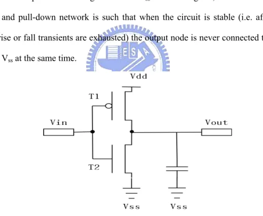
(17) supply voltage, fclk is the clock frequency and α0→1 is the node switching activity factor (the average number of times the node makes a power consuming transition in one clock period). Let us analyze each contribution in detail, considering a simple static CMOS gate, an inverter, as a motivating example. Other combinational and sequential gates show a similar behavior. Figure 2-1 shows the structure of the generic static CMOS inverter. The pull-up network is built with PMOS transistors (T1 for the selected inverter) and it connects the output node Vout to the power supply Vdd. Conversely, the pull-down network is composed of NMOS transistors (T2 for the selected inverter) and it connects the output node to the ground node Vss. In CMOS gates, the structure of the pull-up and pull-down network is such that when the circuit is stable (i.e. after the output rise or fall transients are exhausted) the output node is never connected to both Vdd and Vss at the same time.. Figure 2-1: The structure of a CMOS inverter When an input transition causes a change in the conductive state of the pull-up and the pull-down network, the electric charge is transferred from the power supply to the output capacitance CL or from the output capacitance to ground. The transition causes power dissipation on the resistive pull-up and pull-down networks. Let us 7.
(18) consider a rising output transition (see Figure 6-a). Power is by definition Psw (t) = d E(t) / dt = id (t) v (t), where id (t) is the current drawn from the supply and v (t) is the supply voltage Vdd. The total energy provided by the supply is [13]: Tr. Vdd. 0. 0. E r = ∫ id (t )v(t )dt = Vdd ∫ C L dVout = CoutVdd2. where Tr is the time interval long enough for the transient exhaustion. Notice that we implicitly assume that all current provided by Vdd is used to charge the output capacitance. We also assume the output capacitance to be a constant. At the end of the transition, the output capacitance is charged to Vdd, and the energy stored in it is given by: Es = 1/ 2C LVdd2 . Hence, the total energy dissipated by T1 during the 0→1 output transition is: Ed = C LVdd2 − 1 / 2C LVdd2 = 1 / 2C LVdd2 .. (a). (b) Figure 2-2: (a) The 0→1 and (b) 1→0. If we consider the falling output transition (see Figure 6-b), no energy is stored in the output capacitance. For the conservation of the energy, the total energy dissipated 8.
(19) by T2 during a falling output transition is given by Es = 1/ 2C LVdd2 . This derivation leads us to the fundamental expression of the switching power consumption [13]:. Psw = αC LVdd2 f where CL is the load capacitance, Vdd is the supply voltage, f is the clock frequency and α is the node switching activity factor. Factor CL is decided once the manufacture process has been chosen. Decreasing the Vdd factor has a quadratic effect and can be an effective way. However, the supply voltage is usually determined by the system and technology consideration, and decreasing Vdd will accordingly increase the propagation delay. The computing time will be definitely extended by reducing the factor f, clock speed. It is an unacceptable defect to trade performance of embedded system that usually has real-time demands. Moreover, the power of other idle modules cannot be omitted since execution time increases. Therefore, the most important factor that distinguishes power is its dependence on the switching activity. There are two ways to cut-down the switching activity on buses in execution time, 1.. Reducing transaction counts: Reducing requests of memory access is a direct approach to reduce bit transitions on buses. Buses can keep idle and eliminate power consumption since requests are saved. To increase the reusability of transmitted values is a common example of this idea.. 2.. Reducing numbers of switch activities per transaction: Reducing numbers of switch activities per transaction that make the current transmitted bits near previous ones can reduce number of capacitances needed to be driven. Bus masking is a general technique 9.
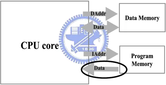
(20) to eliminate variability between two sequential accesses.. 2.3 Baseline System. Our baseline architecture model is as Figure 2-3. The processor sends address request and receives instructions from main memory directly at this baseline system. We find that repeatedly executed instructions will continuously drive the same bus transactions and consume power. Therefore, power consumption of instruction bus is reduced by reducing memory transactions.. DAddr. Data Memory. Data. CPU core. IAddr Data. Program Memory. Figure 2-3: Architecture model of baseline system The power consumption on instruction and address buses all follows the follows the formula for that of CMOS circuit. The power consumption model on buses of the baseline system is. 10.
(21) PowerBaseline = PBUS Dynamic + PBUS Static 2. ∝ ntoggles C LVdd f BUS ∝ ntoggles where PBUS Static , static power dissipatio n can be ignored ntoggles , numbers of bit toggle s on bus C L , load capacitanc es of bus line Vdd , supply voltage f BUS , bus frequency. The average power consumption also concludes the leakage power and the short-circuit power, which are not in our discussion. The static power dissipated by CMOS VLSI gate is in the nanowatt range [1], which is ignored. Using this evaluation metric, we can calculate the power consumption during programs executing. We mention above that the capacitances and supply voltage should remain unchanged. Our design goal is reducing numbers of bit transitions on bus with less power consumption.. 2.4 Previous Research of Power Reduction on Buses. Four previous researches in reducing the switching activities on buses are introduced in the following sections: bus invert encoding scheme [7], BITS (Bus Invert Transition Signaling) encoding scheme [8], Petrov’s bus encoding scheme [10], and register relabeling [9]. As described in Chapter 1, there are two ways to reduce the numbers of switching activities. All belong to reducing numbers of switching activities per transaction. According to the characteristics of buses, bus invert and 11.
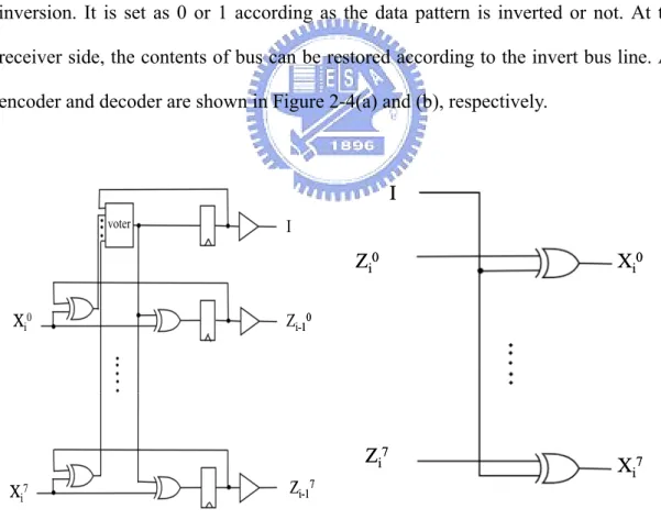
(22) BITS perform well on instruction and data buses. Petrov’s bus encoding scheme and register relabeling can only reduce transactions on instruction buses.. 2.4.1 Bus Invert Power Saving Technique. This method [7] first computes the hamming distance between the present value and the data value on a bus. If the number of transitions between the current pattern on the bus, denoted by Xi, and the previous pattern, denoted by Zi-1, exceeds half the width, the current pattern is transferred with each bit inverted. Otherwise, the current pattern keeps unchanged. An extra bus line, denoted by I, is used to signal the inversion. It is set as 0 or 1 according as the data pattern is inverted or not. At the receiver side, the contents of bus can be restored according to the invert bus line. An encoder and decoder are shown in Figure 2-4(a) and (b), respectively.. I voter. I. Zi0 Xi0. Zi-10. Zi7 Xi7. Xi0. Zi-1. 7. Xi7. Figure 2-4: Schematic diagrams of bus-invert (a) encoder (b) decoder. 12.
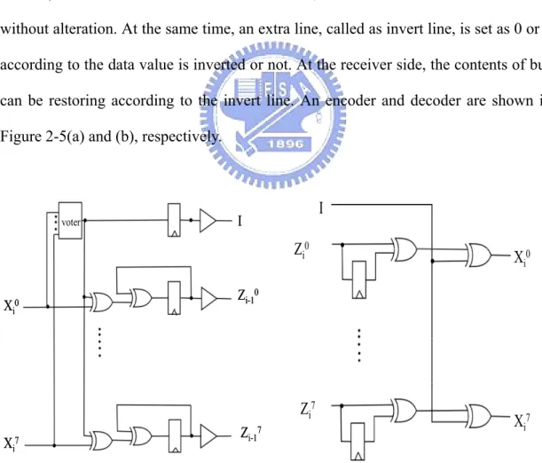
(23) Bus-Invert method presents a trade-off between performance and power dissipation. The performance decreases because the comparator and majority voting circuits increase the area and delay of the data-path. Another trade-off is that an extra I/O pin (invert line) is needed.. 2.4.2 Bus Invert Transition Signaling Power Saving Technique. This method [8] first computes the 1s in present value Xi on a bus. If the number of 1s in Xi is larger than half the bus width, then each bit of Xi is inverted (with line I set to 1) and then transition-encoded. Otherwise, each bit of Xi is transition-encoded without alteration. At the same time, an extra line, called as invert line, is set as 0 or 1 according to the data value is inverted or not. At the receiver side, the contents of bus can be restoring according to the invert line. An encoder and decoder are shown in Figure 2-5(a) and (b), respectively.. voter. I. I. Zi0 Xi0. Zi-10. Zi7 Xi7. Xi0. Zi-17. Xi7. Figure 2-5 : Schematic diagrams of BITS (a) encoder (b) decoder Bus-Invert Transition Signaling method presents a trade-off between 13.
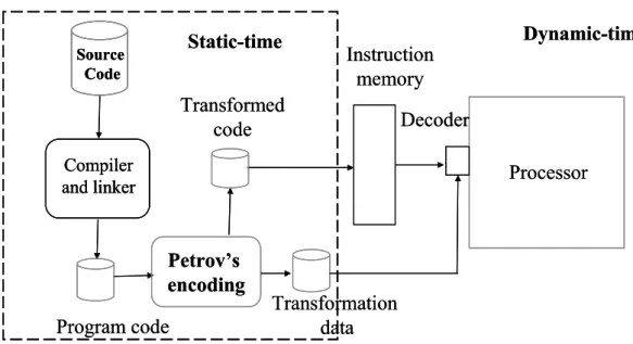
(24) performance and power dissipation. The performance decreases because the comparator and majority voting circuits increase the area and delay of the data-path. Another trade-off is that an extra I/O pin (invert line) is needed.. 2.4.3 Petrov’s Bus Encoding Power Saving Technique. Petrov’s bus encoding scheme [10] minimizes the total number of transitions on each bit line of data bus from the instruction memory. Therefore, it can reduce the significant power overhead in processor memory communication. This technique is an application-specific dynamic customization for power minimization in the instruction memory’s data bus. Fundamentally, it uses application-specific information to identify optimal power encoding. The encoded instructions reside in memory, and the processor core receives information about the transformation, either when loading the program or when running the software. The processor’s fetch module uses this information to efficiently restore the original bit sequence on each bus line. Figure 2-6 is design flow of this bus encoding method.. 14.
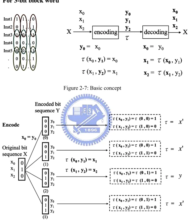
(25) Static-time. Source Code. Dynamic-time. Instruction memory. Transformed code. Decoder. Compiler and linker. Processor. Petrov’s encoding Program code. Transformation data. Figure 2-6: Design flow of Petrov’s bus encoding scheme. An application typically spends most of its execution time on a few tight loops. Data bus transfers form instruction storage causes many transitions on each bus line. Vertical bit sequences are targeted for this encoding method that independently considers the bit streams associated with each bus. Consider arbitrary bit sequence X = {…, xn+3, xn+2,…, xn-3,….}. They want to find alternative bit sequence Y = {…, yn+3, yn+2,…, yn-3,….} and transformation τ such that the total number of bit flips in Y is less than in X. and X =τ(Y). The bit sequence length can be arbitrarily long. Identifying a single transformation that maps Y to X and providing the necessary hardware support would permit restoration of the original bit sequence. Given block size k, identifying the optimal subset of transformations requires finding transformationτ(xi-1 , yi) for every block word, such that X =τ(Y) and the number of bit transitions in Y is minimal. Therefore, this transformation must satisfy the following system of equations:. x0 = y0 ; xi = τ (x i-1 , y i ), i ≤ k This system of equation must be solved with variable τ for all 2k block words 15.
(26) for the sake of finding optimal transformation τ of each block word. Figure 2-7 illustrates the basic concept of Petrov’s encoding scheme. Figure 2-8 and Figure 2-9 are encoding and decoding examples for 3-bit block word.. For 3-bit block word Inst1 1 1 . . . 0 Inst2 0 1 . . . 1. X. Inst3 1 0 . . . 1 Inst4 0 0 . . . 0 Inst5 0 0 . . . 1 .. 0 0...1. .. 0 1...0. x0 x1 x2. encoding. y0 y1 y2. τ. decoding. x0 x1 x2. X. y0 = x0. x0 = y0. τ(x0 , y1) = x0. x1 = τ(x0 , y1). τ(x1 , y2) = x1. x2 = τ(x1 , y2). Figure 2-7: Basic concept Encoded bit sequence Y Encode x0 = y 0 Original bit sequence X x0 0 x1 1 x2 0. τ( x0 , y1) =τ (0 , 0) = 1. 0 y0 0 y1 0 y2 (0) 0 y0 0 y1 1 y2 (1) 0 y0 1 y1 0 y2. τ( x1 , y2) =τ (1 , 0) = 0. τ( x0 , y1) =τ (0 , 0) = 1 τ( x1 , y2) =τ (1 , 1) = 0. τ=. x'. τ=. x'. τ=. y. τ=. x'. τ (x0 , y1) = x1 τ (x1 , y2) = x2. τ( x0 , y1) =τ (0 , 1) = 1 τ( x1 , y2) =τ (1 , 0) = 0. (2) τ( x0 , y1) =τ (0 , 1) = 1. 0 y0 1 y1 1 y2. τ( x1 , y2) =τ (1 , 1) = 0. (1). Figure 2-8: 3-bit block word encoding example According to Figure 2-8, we can construct Table 2-1 that shows the transformation mapping for 3-bit block word. It uses three transformation functions. Therefore, transformation data per block word is 2 bits. 16.
(27) Table 2-1: 3-bit block word transformation. Decode. x0 = y0 x1 = τ (x0 , y1). Encoded bit sequence Y. x2 = τ (x1 , y2). y0 0 y1 0 y2 0. x 0 = y0 = 0 τ=. x'. x1 = τ (x0 , y1) = x0 ' = 1 x2 = τ (x1 , y2) = x1 ' = 0. Original bit sequence X 0 x0 1 x1 0 x2. Figure 2-9: 3-bit block word decoding example Table 2-2 shows the transformation mapping for 4-bit block word. It uses five transformation functions. Therefore, transformation data per block word is 3 bits.. 17.
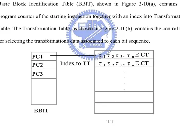
(28) Table 2-2: 4-bit block word transformation. The hardware support of this implementation is presented in Figure 2-10. The Basic Block Identification Table (BBIT), shown in Figure 2-10(a), contains the program counter of the starting instruction together with an index into Transformation Table. The Transformation Table, as shown in Figure 2-10(b), contains the control bits for selecting the transformations data associated to each bit sequence. τ1τ2τ3..τn E CT. PC1 PC2. Index to TT. τ1τ2τ3..τn E CT . . . .. PC3. BBIT TT. Figure 2-10: Hardware support Suppose that there are N instructions in a basic block, and each instruction is 32 bits. When the block size is four bits, the number of transformation data for a basic block is ⎡( N − 1) / 3⎤ × 32 .. 18.
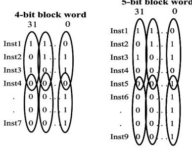
(29) 5-bit block word 0 31. 4-bit block word 0 31. Inst1 1. 1...0. Inst1 1. 1...0. Inst2 0. 1...1. Inst2 0. 1...1. Inst3 1. 0...1. Inst3 1. 0...1. Inst4 0. 0...0. Inst4 0. 0...0. Inst5 0. 0...1. Inst6 0. 0...1. .. 0. 0...1. .. 0. 0...1. .. 0. 0...1. Inst7 0. 0...1. .. 0. 0...1. Inst9 0. 0...1. Figure 2-11: 4-bit and 5-bit block words example We let TTsize denote transformation table size. According to Figure 2-11, we can compute the TTsize as follows:. TTsize = ⎡( N − 1) / 3⎤ × 32 × 3bits. [( N − 1) / 3]× 32 × 3bits ≤ TTsize ≤ [( N − 1) / 3 + 1]× 32 × 3bits 32( N − 1)bits ≤ TTsize ≤ 32( N + 2)bits When the block size is five bits, the transformation data for a basic block is ⎡( N − 1) / 4⎤ × 32 .. TTsize = ⎡( N − 1) / 4⎤ × 32 × 3bits. [( N − 1) / 4]× 32 × 3bits ≤ TTsize ≤ [( N − 1) / 4 + 1]× 32 × 3bits 24( N − 1)bits ≤ TTsize ≤ 24( N + 3)bits The bit transition reduction is higher for codes with shorter block size. However, having shorter block words leads to higher hardware overhead. Selecting the appropriate block size is a tradeoff between hardware overhead and the solution’s efficacy.. 19.
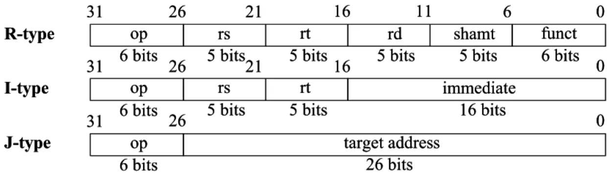
(30) Comparison of Transformation Table Size 35. Transformation Table Size (N-1)bits. 30. 25. 20. Petrov's method 15. 10. 5. 0 2. 3. 4. 5. 6. 7. Block word size (bits). Figure 2-12: Comparison of transformation table size When the block size is four bits, the transformation table size is about equal to the size of total instructions in the basic block. Therefore, block sizes of 5 and 6 bits should receive primary consideration to be compared with our proposed method later.. 2.4.4 Register Relabeling Power Saving Technique. In a typical RISC ISA, register fields are in fixed positions within the instruction encoding and occupy a significant part of the instruction word. Figure 2-13 shows MIPS instruction format. These general-purpose registers are interchangeable.. 20.
(31) 31 R-type 31 I-type 31 J-type. op 6 bits op 6 bits. 26. 21. 26. rs 5 bits 21 rs 5 bits. 26. 16 rt 5 bits. 16. 11. 6. rd 5 bits. funct 6 bits. shamt 5 bits. rt 5 bits. op 6 bits. 0. immediate 16 bits. 0. target address 26 bits. Figure 2-13: MIPS instruction format The basic concept of register relabeling [9] is to minimize the bit changes of the register fields during instruction fetches by re-assigning register numbers. Naïve register labeling can incur significant bit transitions in consecutive register fields of the instruction word. Since general-purpose registers are interchangeable, this technique reassigns registers so that the bit transitions within the register index streams are minimized. Figure 2-14 shows an example code fragment. It could achieve reduction in bit transition with no performance penalties.. Bit transitions on Register fields:. 7 4 +. 5. add sub sub mul. r3, r6, r3, r4,. r2, r3, r2, r4,. r4 r5 r6 r5. r3 r6. r6 r7. add sub sub mul. r6, r7, r6, r4,. r2, r6, r2, r4,. r4 r5 r7 r5 +. 3 4 3 10. 16 Figure 2-14: Example code fragment. 21. 0.
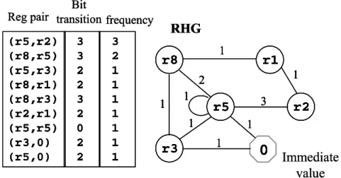
(32) Bit Reg pair transition frequency (r5,r2) (r8,r5) (r5,r3) (r8,r1) (r8,r3) (r2,r1) (r5,r5) (r3,0) (r5,0). 3 3 2 2 3 2 0 2 2. 3 2 1 1 1 1 1 1 1. RHG 1. r8. r1 1. 2 1. 1. 3. r5. 1. r3. r2. 1 1. 0 Immediate value. Figure 2-15: (a) Frequency distribution of register pairs (b) Register Histogram Graph. Register Histogram Graph (RHG) is introduced for capturing the utilization frequency and relation between register pairs. RHG nodes correspond to registers and literals. Each RHG edge annotated with the frequency of occurrence. Figure 2-15 (a) shows all pairs of registers and literal-register pairs, which appear in the code and the quantity of each pair. Figure 2-15 (b) is one RHG example. The following algorithm utilizes the RHG to reassign the register name.. Algorithm Iterate through the edges starting from the most frequent ones Rename the registers yet unassigned so that hamming distance to all their assigned neighbors in the graph is minimized Figure 2-16 shows the RHG after register relabeling.. 22.
(33) R5 1. 1. R7. 2 3. R1. 1. R4. Unassigned Register Names. 1. R1 R2 R3 R4 R5 R6 R7. 1. R3. 1 1. 0. Number of transitions reduced from 28 to 12 ! Figure 2-16: RHG after register relabeling The register fields that occupy the instruction set encoding are small than 50%. Moreover, the best assignment can only be one hamming distance for each register pair with different registers. Therefore, when the distribution of all register pairs is very skew, or the numbers of some register pairs are very large, there is some improvement space to further reduce bit transitions.. 2.4.5 Summary of Previous Researches. This section gives a brief summary of previous researches mentioned above. The bus-invert method performs well when patterns to be transmitted are randomly distributed in time and no information about pattern correlation is available. Therefore, the method seems to be appropriate for encoding the information traveling on data buses. Major drawbacks of this approach are related to the required redundant bus line and the overhead due to the logic to implement the voter to decide whether the Hamming distance exceeds N / 2. Also, an additional bus line is required to mark if the buses are inverted or not. Moreover, it appropriates for narrow bus. BITS method can efficiently reduce bit transitions when the transition signaling is biased. Moreover, it appropriates for narrow bus. But it also needs a complicated 23.
(34) encoder and a redundant control line. Petrov’s bus encoding scheme is efficient for programs include frequently executed loops and no encoder requirement, but it need large transformation table that stores transformation data and a complicated decoder. Register relabeling can only reduce bit transitions on register fields. It’s not very efficient method because register fields that occupy the instruction set encoding are small than 50%. Moreover, the best assignment can be only one hamming distance for each register pair with different registers. We observe that the distribution of various register pairs is highly skewed, or the numbers of some register pairs is very large. Taking advantage of this skew, there is some improvement space so as to further reduce bit transitions. And it has an advantage that does not need extra hardware overhead. These four techniques are compared in Table 2-3. The symbol “—” means that there is not this kind of extra hardware requirement. We also list our design here to compare with these methods. The detail description of our design will be discussed in the next chapter. Table 2-3: Extra hardware comparison of the power saving techniques BI. BITS. Petrov’s. Register. Our design,. method. relabeling. BIBITS. Encoder complexity. High. High. —. —. —. Decoder complexity. Low. Low. High. —. Medium. —. —. Large. —. Small. Table size. From the next chapter, a new power reduction scheme that provides the abilities of low power and real-time execution will be proposed. The proposed method is 24.
(35) designed for reducing the power consumption on instruction buses. It divides the power-saving scheme into two phases so that process the complicated phase is able to be processed in the software offline.. 25.
(36) Chapter 3. Design of BIBITS Bus Encoding. The design of reducing the switching activity on system-level buses through the application of dedicated encoding schemes is discussed in this chapter. The aim is to propose innovative encoding techniques combined with register relabeling to minimize the total number of bit transitions on each bit line on the data bus from the instruction memory. Figure 3-1 shows the static-time design flow of BIBITS bus encoding scheme with modified register relabeling. We add modified register relabeling step before BIBITS bus encoding scheme.. Source Code. Traditional Compiler/ Register Allocator. Transformed code. Code Generation. BIBITS Encoding. Transformation data. Modified Register Relabeling. Linker. Program code. Figure 3-1 Static-time design flow of BIBITS bus encoding scheme with modified register relabeling. BIBITS encoding scheme for power saving is discussed in Section 3.1. Based on the design of BIBITS encoding scheme, a further technique, BIBITS encoding scheme with register relabeling, is introduced so as to further reduce power consumption in Section 3.2. A basic block selection algorithm used in our design is proposed in Section 3.3. 26.
(37) 3.1 BIBITS Bus Encoding Scheme. Our design, BIBITS bus encoding scheme, is applied only for the major application loop. This method is divided as three phase: BIBITS encoding method algorithm, hardware mechanism, and basic-block selection algorithm. The part of BIBITS encoding method algorithm introduces how to encoding instruction at static time .The hardware mechanism of our design includes decoding-control logic, basic block identification table and transformation table. The part of basic-block selection algorithm is responsible to choose the most important basic-blocks to lower numbers of bit transitions on bus.. 3.1.1 BIBITS Encoding Method Algorithm. First, all basic blocks of the original program are encoded. Because we intend to combine an encoding method with register relabeling, we let the partition size equal to register field size. In other words, the partition size is five bits. Bit 6 and bit 30 are not encoded because bit 30 has less bit transitions by statically analysis. An instruction format is partitioned like Figure 3-2 so as to let one register field exactly be one partition. Each partition of current instruction is compared with the corresponding partition of previous instruction, and then the best encoding function that can reduce the most bit transitions for each partition is chosen.. 27.
(38) Basic Block B1 B3. B2 B4. 1 0 1010. 00001. 00100. 00101. 00101. 1. 11000. 0 1 0101. 00011. 00101. 00111. 00000. 0. 11011. 1 0 0001. 00010. 00110. 00101. 00001. 1. 11111. 0 0 1001. 00001. 00101. 00100. 00000. 1. 00111. 1 0 1001. 00111. 00011. 00101. 00001. 1. 11011. 31. 0. 5 bits partition. Figure 3-2: BIBITS encoding method Let HDn,p be the Hamming distance between partition Bn,p and Bn-1,p given by HDn,p = # 1s of (Bn,p ♁ Bn-1,p) The objective function then is to minimize. ∑ ∑ N. 6. n =1. p =1. HDn , p. xi: Original current pattern yi: Encoded current pattern yi-1: Encoded previous pattern encoder xi. yi = xi op yi-1. yi-1. decoder. yi. xi = yi op yi-1. Figure 3-3: BIBITS encoding basic concept Table 3-1 shows us sixteen functions of two Boolean variables. Table 3-1: The 16 functions of two Boolean variables. 28. xi.
(39) According to Table 3-1, only four functions that can be used to decode the encoded partition by using the same function which is used in the encoding step is chosen, as illustrated in Figure 3-3. In other words, the relation between encoder and decoder must satisfy the following equation.. ((xi op yi-1) op yi-1) = xi Only four functions satisfy the Boolean expression from table of 16 binary operators, and also that none of the other 12 functions in the table has this property. Therefore, four selected functions are identify, invert, XOR, and XNOR. Since it is an NP-complete problem to find an optimal assignment function, we propose a heuristics algorithm that can be applied to find better encodings.. BIBITS encoding method algorithm is –Sequentially choose the best encoding function for each partition –With the contribution ratio of each basic block , we can apply the greedy algorithm to help us select which basic block should be encoded. xi: Original current pattern yi: Encoded current pattern yi-1: Encoded previous pattern. yi-1 01101. yi-1 01101. yi -1 01101. yi-1 01101. yi-1 01101. xi 11110. yi 11110. yi 00001. yi 11011. yi 01100. 3. 1. Bit transition. 3. 3. 2. Figure 3-4: BIBITS encoding example. 29.
(40) 3.1.2 Hardware Support for BIBITS Encoding. The hardware mechanism consists of three main modules: basic-block identification table, transformation table and decoding hardware. The block diagram of the proposed method is shown in Figure 3-5. The blocks inside the dotted line are our designed circuits, the decoding-control logic, that contain four elements: instruction fetcher, basic block identification table, transformation table, and decoder. This hardware mechanism may be combined with processor core into a single chip.. Figure 3-5: System architecture with BIBITS encoding. 3.1.3 Decoding-Control Logic. The decoding-control logic is responsible for sending instructions to processor from memory. It first fetches instructions from memory and then determines if the fetched instruction is an encoded instruction. If the fetched instruction is an encoded 30.
(41) instruction, the original instructions will be gathered from the decoder. The decoding-control logic consists of four elements: instruction fetcher, basic block identification table, transformation table, and decoder.. 1. Instruction Fetcher: The instruction fetcher receives the program-counter address request from processor. 2. Basic Block Identification Table (BBIT): The basic block identification table stores the program counter value of the starting instruction and an index that points to the first entry in the transformation table for this basic block. The number of entries in this table corresponds to the number of encoded basic blocks for the particular application loop.. Figure 3-6: BBIT and Transformation Table. 3. Transformation Table (TT): The transformation table stores transformation data τn associated with each encoded partition from the instruction memory. A TT entry contains. 31.
(42) the control bits for selecting the transformation associated with each partition. The hardware structure asserts the end bit field (E) in the TT entry for entries corresponding to the last partition word in a given basic block. 4. Decoder: The decoder receives the control bitsτn from TT , and selects decoder function to restore each partition of encoded instructions. The circuit diagram of the decoder is shown in Figure 3-7.. Figure 3-7: Decoder circuit Decoding Procedure The decoding procedure of this architecture is as follows. 1.. CPU sends program counter value to decoding controller.. 2.. Instruction fetcher access memory for reading instruction.. 3.. Search basic block identification table to see if there is an entry that is equal to the program counter value. I.. Yes; the fetched instruction is an encoded instruction. Send the value of the found entry to the transformation table. Go to Step 4.. II.. No; the fetched instruction is directly passed to CPU core. Go to Step 1.. 4.. Use transformation index to read transformation data in transformation table and send to decoder and check if entry boundary bit it true. 32.
(43) I.. Yes; this transformation table entry is finished, and thus the next instruction should be a non-encoded instruction. Go to Step 1.. II. 5.. No; next instruction is still an encoded instruction.. Go to Step 4.. 3.2 Modified Register Relabeling for BIBITS Bus Encoding Scheme. Based on the design of the BIBITS encoding scheme, there is still a chance to reduce power consumption in advance. A further technique, modified register relabeling, is introduced to further reduce power consumption in this section. The idea of this is come from the observation of program-execution trace. When program is executed, processor often executes sequence of instructions repeatedly. This sequence of instructions is known as loop. A loop contains either one or more basic blocks. Therefore, the distribution of register pairs is very skew. According to Figure 3-8, we find that the best assignment can only be one Hamming distance for each register pair with different registers. However, there are still a lot of bit transitions when frequency of the register pair is very large. If he Hamming distance of the register pair can further be reduced from one to zero, a lot of bit transitions will be reduced. Therefore, modify original register relabeling method is proposed to resolve this problem. The difference between our proposed register relabeling algorithm and original register relabeling algorithm is that we consider that register relabeling is able to be combined with BIBITS bus encoding scheme, such that the best assignment of register relabeling will be one register pair that is zero Hamming distance. We see the following Figure 3-8, for example, R2 and R5 are 33.
(44) assigned as R2 and R3 that is one Hamming distance. And it is a best assignment case in original register relabeling method. But our modified register relabeling method assigns one inverse register pair that is R26 and R5. After applying BIBITS bus encoding step, this register pair will become R5 and R5, and the Hamming distance of this register pair becomes zero.. Original Register Relabeling R5 (00101). R2 (00010). Modified Register Relabeling R2 (00010). R5 (00101) Modified Relabeling. Relabeling. R26 (11010). R5 (00101). BIBITS encoding. R2 (00010). R3 (00011). R5 (00101). Bit transition = 1. Y = X′. R5 (00101). Bit transition = 0. Figure 3-8: Comparison of original register relabeling and modified register relabeling for BIBITS bus encoding. Figure 3-9(a) shows us register pairs frequency of some program. RHG captures the utilization frequency and relation between register pairs. Nodes of the RHG correspond to registers and literals, and edge weight corresponds to frequency. Iterate through the edges starting from the most frequent ones. The following Figure 3-9 (b) is an example of RHG.. 34.
(45) Bit Reg pair transition frequency (r5,r2) (r8,r5) (r5,r3) (r8,r1) (r8,r3) (r2,r1) (r5,r5) (r3,0) (r5,0). 3 3 2 2 3 2 0 2 2. RHG. 6 4 2 2 2 2 2 2 2. 2. r8. r1 2. 4 2. 2 2. r3. 6. r5. r2. 2 2. 0. Figure 3-9: (a) Register pairs frequencies of some program (b) An example of register histogram graph. The detailed modified register relabeling for BIBITS bus encoding algorithm is –Iterate through the edges starting from the highest weight edgei ‧If two nodes of edgei have not been assigned a new register name, then assign one inverted register pair Rx and R31-x, such that H.D.(BIBITS(Rx,R31-x))=0. If one inverted register pair is not found, then assign one register pair Rx and Ry, such that H.D.(BIBITS(Rx, Ry)) is minimized. ‧If one node of edgei has been assigned Rx, then assign Ry to another node, such that H.D.(BIBITS(Rx, Ry)) is minimized. ‧If all nodes of edgei have been assigned new register names, then process the next edge.. 35.
(46) 3.3 Basic Block Selection Algorithm. Our selection algorithm is applied to analyze programs-execution behavior. We analyze and calculate the numbers of bit toggles and execution counts of each basic block. The task of determining an optimal basic blocks for a given programs is known to be NP-complete in the size of the programs. However, many heuristics have sprung up that find near optimal solutions to the problem, and most are quite similar. The key idea of the encoded basic-block selection algorithm is to select the most frequent basic blocks to be encoded. We analyze the program-execution trace with this algorithm. First, we identify every basic block, and then we calculate the occurrence frequency and numbers of bit transitions of each basic block occurs on bus. After the trace analyzing, each basic block has three parameters: numbers of instruction of this basic block (length of this basic block), numbers of execution counts, and numbers of bit transitions. Each basic block has a contribution value measured as the product of numbers of execution counts and numbers of bit transitions. We can compute the contribution as the contribution value divided by the length of this basic block. The greedy algorithm with the contribution ratio of each basic block is applied to help us select which basic block should be encoded. The selection algorithm is shown as follows. Suppose that there is a set BB = {1,2,...n} of n basic blocks in the program. Each basic block has a contribution value:. Contribution =. ExecutionCounts ⋅ BitToggles . (EQ1) Length. Assumption that transformation table size is S. The greedy-basic-block selector 36.
(47) algorithm is. TT : Transformation Table BB : Basic Block TD(BB{i}): Transformation data of basic block. Greedy − Basic − Block − Selector (n, CR ) 1. Let TT as empty 2. Sort set BB by contribution ratio(CR) ↓ of each basic block 3. for i ∈ BB[n] in ↓ order 4. do if Sizeof(TT ∪ TD(BB{i}) ) ≤ S 5. then TT ← TT ∪ TD(BB{i}) 6. return TT. For example, the algorithm can be illustrated as Figure 3-10. Figure 3-10: An example of greedy-basic -block selector algorithm. 37.
(48) Table 3-2: Computing contribution ratio of each basic block Frequency Bit Toggles. Length. Contribution. CR. BB1. 3. 43. 4. 129. 32.25. BB2. 2. 55. 4. 110. 27.5. BB3. 2. 30. 3. 60. 20. After analyze the trace of program execution, the set BB has three elements: Basic-Block 1, Basic-Block 2, and Basic-Block 3. The parameters of these three basic blocks are shown as Table 3-2. The selection priority is first BB 1, then BB 2, and BB 3 is the last one.. 38.
(49) Chapter 4. Simulation and Analysis. Benchmark programs are first discussed in this chapter. Simulation methods are then introduced in this thesis, including the toolsets, simulation flow, simulation parameters and evaluating factors.. 4.1 Experimental Benchmarks. We perform experiments for the following benchmarks for evaluating the efficiency of encoding in bus transition reduction. These six DSP or numerical-computation kernels that represent code frequently encountered in many embedded system products. Table 4-1 gives a summary of our choice of benchmarks. Table 4-1: Benchmark Function Name. Description. Mmul. A matrix multiplication of 100 × 100 element matrices.. SOR. Successive over-relaxation on a 256 × 256 element matrix.. EJ. Extrapolated Jacobi-iterative method on a 128 × 128 entry grid.. FFT. Fast Fourier transform with a 256-bit sample block size.. Tri. Tri-diagonal system solver on a 128 × 128 element matrix.. LU. Lower/upper triangular matrix decomposition algorithm on a 128 × 128 element matrix.. The size and basic block number of each benchmark program is presented in Table 4-2.. 39.
(50) Table 4-2: Benchmark program size and numbers of each basic block Program. Program size (Bytes). Number of Basic Block. Mmul. 304. 13. Sor. 1300. 14. Ej. 1500. 22. FFT. 1152. 65. Tri. 1252. 9. LU. 3376. 34. 4.2 Experimental Methods. The experimental toolset we used in this simulation are described in this section. These tools are either MIPS® SDE Lite, a free subset of the MIPS Software Toolkit [11][12], or created by us. We wrote a simulation tool so that we could do basic block selection, modified register relabeling and BIBITS encoding scheme. And we also could evaluate the number of bit transitions on all the lines of the instruction bus. We also list the experimental flow, the experiments we planned to do, and simulation parameters we referred.. 4.2.1 Experimental Toolset. Experimental environment is divided into three sub-environments: z. Code Generation phase: The purpose of this sub-environment is to compile the executable machine codes for the benchmark programs. We adopt MIPS® SDE Lite version 5.03.06.[12] to build the MIPS ELF (Executable and Linkable Format) image format for each benchmark program. 40.
(51) z. Transformation Table Building phase: This sub-environment includes a transformation table builder and a code-rebuilder. The transformation table builder scans the program execution trace running under the GNU MIPS CPU Simulator and builds the transformation table for each benchmark program. The code-rebuilder rebuilds selected basic-blocks of programs by BIBITS encoding.. z. Result Calculation phase: The final sub-environment includes the modified simulator and a bit transition calculator.. We have adopted and developed the complete experimental toolset consisting of individual tools that accomplish specific tasks respectively for constructing the experimental environment. Table 4-3 lists all tools composing the experimental toolset. Table 4-3: Experimental toolset descriptions Tool Name. sde-gcc. Description SDE’s version of the Free Software Foundation’s ANSI-compatible GNU C Compiler compiling C source code. This version incorporates superb optimization for RISC processors, such as MIPS architecture processors. SDE’s version of the GNU linker and loader links the object. sde-ld. files necessary for building MIPS ELF files of the components in the benchmark suite.. sde-run. The GNU MIPS CPU simulator executes the MIPS ELF image files. It could trace the execution behaviors of the benchmark programs.. BB-sel. The Basic Block Selector that builds the recovery dictionary with dictionary building rules by scanning the MIPS program execution trace.. code-rebuild. The code-rebuilder rebuilds the program with the transformation table provided from the transformation table 41.
(52) builder. modsde-run. The modified GNU MIPS CPU simulator to execute the encoded programs and calculate the power needed for this architecture.. 4.2.2 Experimental Flow. The experimental flow, the experimental toolset and intermediate files, such as object files, MIPS ELF files, etc., are shown in Figure 4-1. By a horizontal dotted line, this figure is divided into three sub-figures representing the three experimental sub-environments representing the three experimental sub-environments.. 42.
(53) Benchmarks (.c). Code Generation C Compiler (sde-gcc). Assembly code ( .S ) Reg. relabeler. Assembly code ( .S ). (reg-relabel). Linker (sde-ld). Input Data. ELF. GNU Tracer. Execution Trace. (sde-run). Build Transformation Table. BB-Selector ( BB-Sel). TT Files (.tt). ELF. Code-Rebuilder. Encoded Files (.coded). (Code-rebuild). Input Data. TT Files (.tt). Modified-Tracer (Mod-run). Result Calculator Bit transition. Figure 4-1: Experimental flow by using our experimental toolset. 43.
(54) The complete experimental flow is described as follows: 1.. The MIPS C compiler (sde-gcc) compiles the source files (.c) of the benchmark programs into its corresponding object files (.o).. 2.. The register relabeler (reg-relabel) adjusts register name to reduce the bit transitions of the instruction register fields.. 3.. The MIPS C linker (sde-ld) links the object files necessary for building MIPS ELF files of the components in the benchmark suite.. 4.. The GNU MIPS CPU Simulator (sde-run) traces the ELF files with input data and then output the execution instructions and the corresponding program counters (PC value).. 5.. The Basic Block Selector (BB-sel) scans execution trace and produces the transformation table that contains selected basic block and encoding information.. 6.. According the transformation table files, the code-rebuilder build the MIPS machine code files.. 7.. The modified GNU MIPS CPU Simulator (modsde-run) executes the coded programs with transformation tables and input data. It also calculates the bit transitions for executing these programs.. 4.2.3 Designing Experiments. The transformation table builder (TTbuild) and the modified tracer (modsde-run) are the core tools in the entire experimental toolset because they are the tools actually analyzing the execution trace and we can evaluate the power consumption of each benchmark. In our simulation, we evaluate the bit transitions of these conditions: 44.
(55) z. Base system architecture. This is the simply architecture with only the processor and instruction memory. The instructions are always fetched from the instruction memory.. z. Bus-invert encoding scheme. This is the power reduction technique mentioned in Chapter 2. We implement this architecture to compare the results between this approach and ours.. z. BITS bus encoding scheme. This is the power reduction technique mentioned in Chapter 2. We implement this architecture to compare the results between this approach and ours.. z. Register Relabeling. This is the power reduction technique we mentioned in tChapter 2. We implement this to compare the results between this approach and ours.. z. Petrov’s bus encoding scheme. This is also the power reduction technique we mentioned in Chapter 2. We implement this architecture to compare the results between this approach and ours.. z. BIBITS bus encoding scheme. This is our design that we execute the coded program with the recovery dictionary.. z. BIBITS bus encoding scheme with original register relabeling. This is our design that we apply original register relabeling before BIBITS bus encoding scheme stage.. z. BIBITS bus encoding scheme with modified register relabeling. This is our design that we apply modified register relabeling before BIBITS bus encoding scheme stage.. The bit transitions effects are evaluated with different transformation table sizes 45.
(56) in Petrov’s bus encoding scheme and our proposed BIBITS bus encoding scheme.. 4.3 Simulation Results and Analyses. Experimental results obtained from evaluating power consumed by the benchmark programs as described above are presented in this chapter. The bit transitions reduction by various techniques for each benchmark programs is first evaluated. The bit transitions reduction of our proposed BIBITS and Petrov’s bus encoding scheme are then evaluated in different transformation table sizes. Notice that the results of bit transition are all normalized to those of the base system.. 4.3.1 Bit Transition Reduction of Different Techniques. Our approach’s effectiveness is measured by observing the reduction of transition on the data bus to the instruction memory. We ran simulation using a typical embedded processor as the baseline system architecture. We used six DSP or numerical-computation benchmarks that represent code frequently encountered in many embedded products. Figure 4-2 displays the bit transition reduction by applying different techniques in six different benchmark programs. There are seven techniques applied in this figure: Bus-invert, BITS, register relabeling, Petrov’s bus encoding scheme, BIBITS bus encoding scheme, BIBITS with original register relabeling (ORR+BIBITS), and BIBITS with modified register relabeling (MRR+BIBITS). Petrov’s bus encoding scheme and relative BIBITS bus encoding schemes need use transformation tables. This experiment selected all basic blocks of each program to be encoded. In other 46.
(57) words, the transformation table size is unlimited.. Figure 4-2: Transition reduction of different techniques. Experimental results indicate that reductions in bit transition of Bus-invert method are not very good. It also shows that reductions in bit transition of our proposed BIBITS encoding scheme range around 56% to 61% except for the fft program. Assume that there are N instructions in some basic block. What about actual transformation table size use by Petrov’s bus encoding scheme and BIBITS bus encoding scheme when all basic blocks are encoded? Results of these are presented in Table 4-4. Obviously, the table size of BIBITS bus encoding scheme is only a half of Petrov’s bus encoding scheme. Table 4-4: Comparison with transformation table size Method Petrov’s bus encoding (4-bit block word). Transformation data number ⎡( N − 1) / 3⎤ × 32. Transformation table size (bits). ⎡( N − 1) / 3⎤ × 32 × 3bits ≅ 32 N − 32bits. 47.
(58) Petrov’s bus encoding (5-bit block word). ⎡( N − 1) / 4⎤ × 32. Petrov’s bus encoding (6-bit block word). ⎡( N − 1) / 5⎤ × 32. BIBITS bus encoding. (N-1)×6=6N-6. ⎡( N − 1) / 4⎤ × 32 × 3bits ≅ 24 N − 24bits. ⎡( N − 1) / 5⎤ × 32 × 3bits ≅ 19.2 N − 19.2bits (6N-6)×2=12N-12bits. BIBITS bus encoding scheme is combined with register relabeling technique so as to further reduce bit transitions. First, original register relabeling is applied before doing BIBITS bus encoding scheme. However, total bit transitions of some programs applied BIBITS bus encoding scheme with original register relabeling are bigger than these applied only BIBITS bus encoding scheme. Resolving this problem requires proposing a modified register relabeling method applied before doing BIBITS bus encoding scheme. According to the result of this experiment, this method can efficiently resolve this problem. Applying register relabeling before BIBITS bus encoding scheme could further reduce bit transitions without increasing extra hardware overhead. While all basic blocks are encoded, transformation table size of “MRR+BIBITS” bus encoding scheme is about a half of Petrov’s bus encoding scheme (5-bit block word). Achieve 64% average bit transition reduction as compared with base-line system. Further reduce 31% average bit transitions as compared with total bit transitions of Petrov’s method (5-bit block word). Moreover, the decoder hardware is more uncomplicated than Petrov’s. In Section 5.2, experiment results of BIBITS bus encoding scheme and Petrov’s bus encoding scheme (5-bit block word) will be presented with different transformation table sizes in detail.. 48.
(59) 4.3.2 Bit Transition Reduction of Techniques with Different Transformation Table Sizes. In the Petrov’s bus encoding scheme (5-bit block word) and our proposed BIBITS bus encoding scheme, we will evaluate the bit transitions effects with different transformation table sizes. Figure 4-3 shows the bit transition reduction of mmul program with different transformation table sizes. BIBITS method has higher bit transition reduction than Petrov’s method. Furthermore, when the transformation table size increases to 0.3 Kbytes, BIBITS method reaches about 51% bit transition reduction. However, Petrov’s method can only reaches 0.6% bit transition reduction. These following figures are experiment result of each benchmark program.. Figure 4-3: mmul - Bit transition reduction with different transformation table sizes. 49.
(60) Figure 4-4: sor - Bit transition reduction with different transformation table sizes. Figure 4-5: ej - Bit transition reduction with different transformation table sizes. 50.
(61) Figure 4-6: fft - Bit transition reduction with different transformation table sizes. Figure 4-7: tri - Bit transition reduction with different transformation table sizes. 51.
(62) Figure 4-8: lu - Bit transition reduction with different transformation table sizes We observe that our method has higher bit transitions reduction than Petrov’s bus encoding scheme. Figure 4-9 displays BIBITS detailed experiment results that are average bit transitions reductions for full benchmarks with different transformation table sizes.. Figure 4-9: Average bit transition reduction for full benchmarks with different transformation table sizes 52.
(63) Chapter 5. Conclusion and Future Works. BIBITS bus encoding scheme is proposed to reduce power consumption on program memory bus in this thesis. Moreover, a modified register relabeling algorithm is also proposed to be combined with BIBITS bus encoding scheme so as to further reduce bit transitions. The key idea of our method is to apply a transformation table which stores frequently execution basic block transformation data to make use of repetitions of basic blocks at program execution time so as to reduce bit transitions on program memory data bus. The simulation results show that the overall average switching reduction is 64% over original data and 57% more than original register relabeling scheme only and more than Petrov’s bus encoding scheme about 13~ 20% except for FFT program. Problems arising form FFT program is almost small basic blocks that has only two or three instructions. Petrov’s bus encoding scheme is more suitable for this kind of basic block size. The suitable size of transformation table varies with different programs. Contrary to Petrov’s bus encoding scheme, our proposed scheme need only a half transformation table size to encode all basic blocks. Moreover, our decoder implementation is more uncomplicated than theirs. Therefore, the extra hardware overhead of our proposed is lower than Petrov’s bus encoding scheme. There are still several researches could be further studied. For example, find compiler techniques that can be combined with bus encoding methods to further reduce bit transitions. For example, BIBITS is combined operand swapping with and instruction scheduling. A large number of instructions, such as addition, multiplication, and logic operations, are insensitive to the order of their operands. Consequently, the commutability of certain instructions provides a degree of freedom. In the same way, 53.
(64) instruction scheduling that changes instruction sequences could also provide a degree of freedom. But these pervious compilation techniques did not consider to be combined with bus encoding schemes. However, applying directly these compilation techniques combined with BIBITS encoding scheme maybe result in worse reduction than only applying BIBITS. Therefore, we must think deeply how to integrate and modify these techniques perfectly, such that the closed integrated scheme is able to further reduce total bit transitions.. 54.
(65) Reference [1] S. Wuytack, F. Catthoor, L. Nachtergaele, H. De Man, “Global communication and memory optimizing transformations for low power signal processing systems,” IWLPD-94: ACM/IEEE International Workshop on Low Power Design, pp. 203-208, April 1994. [2] P.R. Panda and N. D. Dutt, “Reducing Address Bus Transitions for Low Power Memory Mapping,” EDTC-96: IEEE European Design and test Conference, pp. 63-67, Paris, France, March 1996. [3] A. Aho, R. Sethi and J. Ullman, Compilers Principles, Techniques and Tools, Addison-Wesley Publishing Company, 1986 [4] N. Weste, K. Enshraghian, Principles of CMOS VLSI Design, a System Perspective. Reading: Addison-Wesley Publishing Company, 1988 [5] A.P. Chandrakasan, S. Sheng, and R.W. Brodersen, “Low-Power CMOS Digital Design,” IEEE Journal of Solid-State Circuits, Vol. 27, No. 4, pp. 473-483, Apr.1992. [6] A. Chandrakasan, R. Brodersen, “Minimizing Power Consumption in Digital CMOS Circuits,” Vol. 83, No. 4, pp. 498-523, Proceedings of the IEEE, April 1995 [7] M.R. Stan, W.P. Burleson, “Bus-invert coding for low-power I/O,” IEEE Trans. on VLSI Systems, Vol. 3, No. 1, pp. 49-58, Mar. 1995 [8] Youngsoo Shin, Kiyoung Choi, Young-Hoon Chang, “Narrow Bus Encoding for Low-Power DSP systems,” IEEE Trans. On VLSI systems, Vol. 9, No. 5, pp. 656-660, Oct. 2001 [9] Huzefa Mehta, Robert Michael Owens, Mary Jane Irwin, Rita Chen, Debashree Ghosh, “Techniques for Low Energy Software,” Low Power Electronics and Design, 55.
數據
+7
相關文件
The articles in this issue of the NET Scheme News will tell you how our English teachers continue to explore different innovative ways to enrich students’ English learning
Other than exploring the feasibility of introducing a salary scale for KG teachers, we also reviewed the implementation of the Scheme in different areas including funding
Recommendation 14: Subject to the availability of resources and the proposed parameters, we recommend that the Government should consider extending the Financial Assistance
此位址致能包括啟動代表列與行暫存器的 位址。兩階段的使用RAS與CAS設定可以
下列關於 CPU 的敘述,何者正確?(A)暫存器是 CPU 內部的記憶體(B)CPU 內部快取記憶體使 用 Flash Memory(C)具有 32 條控制匯流排排線的 CPU,最大定址空間為
電腦內部是使⽤用位元 (Bit) 這個基本單位來表⽰示資料 並儲存於記憶單元 (記憶體) 或輔助記憶單元 (硬碟) 中。.. 每個位元只可以表⽰示
以電腦輸入團員資料 (Excel 格式)
In this thesis, we have proposed a new and simple feedforward sampling time offset (STO) estimation scheme for an OFDM-based IEEE 802.11a WLAN that uses an interpolator to recover
