Low-Capacitance SCR With Waffle Layout Structure
for On-Chip ESD Protection in RF ICs
Chun-Yu Lin and Ming-Dou Ker
Nanoelectronics and Gigascale Systems Laboratory
Institute of Electronics, National Chiao-Tung University, Hsinchu, Taiwan
Abstract — Silicon-controlled rectifier (SCR) has beenused as an effective on-chip ESD protection device in CMOS technology due to the highest ESD robustness. In this work, the waffle layout structure for SCR can achieve smaller parasitic capacitance under the same ESD robustness. With smaller parasitic capacitance, the degradation on RF circuit performance due to ESD protection device can be reduced. The proposed waffle SCR with low parasitic capacitance is suitable for on-chip ESD protection in RF ICs.
Index Terms — Electrostatic discharges (ESD),
radio-frequency integrated circuit (RF IC), silicon-controlled rectifier (SCR).
I. INTRODUCTION
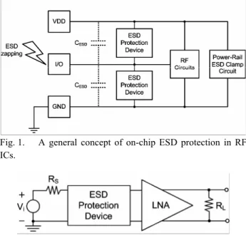
One of the most critical reliability issues for integrated circuits is electrostatic discharge (ESD). A general concept of on-chip ESD protection in RF ICs is illustrated in Fig. 1. The parasitic capacitance (CESD) of ESD protection device is one of the most important design considerations for RF ICs [1], [2]. ESD protection device with conventional layout structure has the parasitic capacitance which is too large to be tolerated for RF ICs. The parasitic capacitance induces RC delay on the signal path and lowers the operating speed of RF ICs. Moreover, the parasitic capacitance loses RF signals from the pad to ground. Noise figure (NF) is an important merit for RF receivers. However, adding ESD protection devices to the RF receiver is adverse to the noise figure. For example, the overall noise figure of the low-noise amplifier (LNA) added with ESD protection device in Fig. 2 is
⋅ LNA
total ESD NF -1 -1 LNA
NF = NF + = L NF
L (1)
where L is the power loss of ESD protection device, and NFLNA and NFESD denote the noise figures of the low-noise amplifier and ESD protection device, respectively. The noise figure of ESD protection device is equal to its power loss because ESD protection device is a passive reciprocal network. To mitigate the RF performance degradation caused by ESD protection device, its parasitic capacitance must be minimized. Therefore, device with large ratio of ESD robustness to parasitic capacitance is
desired. The figure of merit (FOM) used in this paper is VMM/CESD, where VMM is the machine-model (MM) ESD level and CESD is the parasitic capacitance of ESD protection device.
Silicon-controlled rectifier (SCR) device had been reported as RF ESD protection element [3]. The SCR device has very low holding voltage (Vhold, about ~1.5 V in general bulk CMOS processes), so the power dissipation (power≅ IESD×Vhold) located on the SCR device during ESD stress is significantly less than that located on other ESD protection devices, such as the diode, MOS, BJT, or field-oxide device. The SCR device can sustain a much higher ESD level within a smaller layout area in CMOS ICs [4]. A smaller layout area introduces less parasitic capacitance. Thus, using SCR device for RF ESD protection can achieve better FOM of VMM/CESD.
The SCR device was traditionally implemented in the stripe and double-sided layout. Under ESD stresses, ESD current primarily flows through the two edges of SCR,
Fig. 1. A general concept of on-chip ESD protection in RF ICs.
Fig. 2. The diagram of the low-noise amplifier (LNA) with ESD protection device.
while other two edges do not discharge ESD current, but contribute some parasitic capacitance. The SCR device with waffle layout structure can discharge ESD current through four edges. Therefore, the FOM of VMM/CESD can be maximized by using the waffle layout structure.
The MOS transistors in waffle layout structures had been studied [5]. The waffle layout structures for diodes had also been proposed to reduce its parasitic capacitance for ESD protection in high-speed I/O [6]. In this paper, SCR realized in the waffle structure is investigated in a 0.18-µm CMOS process. With the comparison between the conventional stripe SCRs and the waffle SCRs, the improvements from the new proposed waffle SCRs have been confirmed in silicon.
II. SCRSTRUCTURES
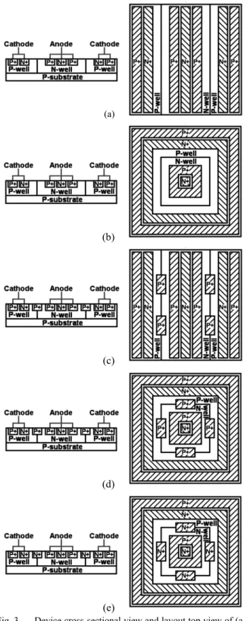
A. SCR With Stripe Layout
The conventional stripe SCR (SSCR) is shown in Fig. 3(a). The discharge path of the SSCR from anode to cathode is P+-diffusion/N-well/P-well/N+-diffusion. The ESD currents only flow through two edges of the N-well. The other two edges of the N-well are unused.
B. SCR With Waffle Layout
In Fig. 3(b), the waffle SCR (WSCR) is proposed to discharge ESD current in four edges of the device. By using the waffle SCR, the ESD protection capability can be enhanced and the FOM can be increased.
C. Modified SCR With Stripe Layout
In Fig. 3(a) and 3(b), the trigger voltage (Vtrigger) of the SSCR or WSCR is the breakdown voltage of the N-well/P-well junction. The modified SCR can improve the turn-on efficiency and reduce the trigger voltage. As shown in Fig. 3(c), the trigger P+-diffusion is added across the N-well/P-well junction in the stripe p-modified SCR (SPMSCR) to reduce the junction breakdown voltage. Since the lager trigger diffusion may increase the parasitic capacitance, the SPMSCR was implemented with different trigger diffusion areas to evaluate the device characteristics and ESD performance.
D. Modified SCR With Waffle Layout
With the trigger P+-diffusion across the N-well/P-well junction, the waffle p-modified SCR (WPMSCR) is shown in Fig. 3(d). The WPMSCR was also implemented with different trigger diffusion areas.
Similarly, the trigger P+-diffusion can be replaced by the trigger N+-diffusion. As shown in Fig. 3(e), the trigger N+-diffusion is added across the N-well/P-well junction of the waffle n-modified SCR (WNMSCR) to characterize the ESD robustness and high frequency performances.
(a)
(b)
(c)
(d)
(e)
Fig. 3. Device cross-sectional view and layout top view of (a) stripe SCR (SSCR), (b) waffle SCR (WSCR), (c) stripe p-modified SCR (SPMSCR), (d) waffle p-p-modified SCR (WPMSCR), and (e) waffle n-modified SCR (WNMSCR).
III.EXPERIMENTAL RESULTS
The aforementioned SCR devices in the traditional stripe layout and in the proposed waffle layout have been fabricated in a 0.18-µm CMOS process. The trigger voltage (Vtrigger), secondary breakdown current (It2), and turn-on resistance (Ron) in the holding region of the fabricated SCR devices have been characterized by the transmission line pulsing (TLP) system. The human-body-model (HBM) and machine-human-body-model (MM) ESD robustness have been evaluated by the ESD simulator.
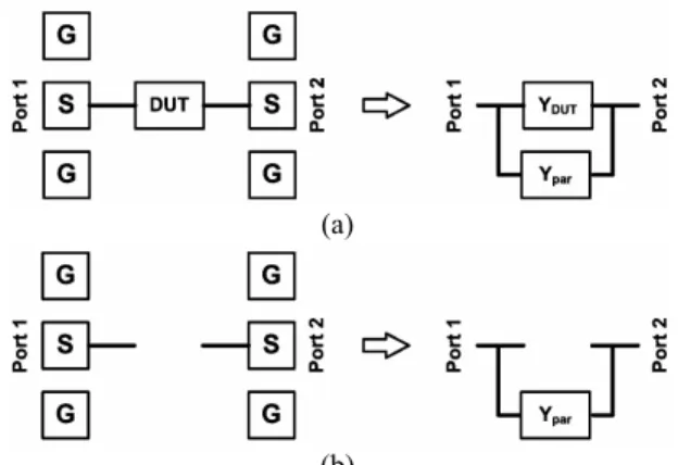
The SCR devices were arranged with ground-signal-ground (G-S-G) pads to facilitate on-wafer measurement. The high-frequency characteristics were obtained from the measured S-parameters under the bias of 0.9 V (VDD/2 in a 0.18-µm CMOS process) by using the vector network analyzer HP 8510C. In order to extract the characteristics of the intrinsic device in high frequency, the parasitic effects of metal interconnects and bond pad must be removed. The test patterns, one including the device under test (DUT) while the other excluding the device under test, as shown in Fig. 4, were fabricated in the same chip. The Y-parameters were obtained from the measured S-parameters. The Y-parameter of the including-DUT pattern is labeled as Ymeas, and the Y-parameter of the excluding-DUT pattern is labeled as Ypar. The intrinsic device characteristics (YDUT) can be obtained by subtracting Ypar from Ymeas. The parasitic capacitance of each SCR was extracted from the Y-parameter of the intrinsic device by using
π 11 ESD Im[Y ]
C =
2 f (2)
where f is the operating frequency.
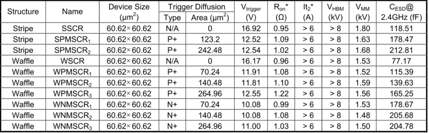
The measured results on the characteristics of the fabricated SCRs are listed in Table I. The trigger voltages among the SCR devices under different layout structures are shown in Fig. 5. Both SSCR and WSCR are triggered at 16-17 V. With the trigger diffusion added into the modified SCRs in the stripe and waffle structures, the trigger voltages were reduced to 10-13 V. The TLP-measured turn-on resistances of the stripe and the waffle SCRs in high-current holding region are as low as ~1 Ω. The secondary breakdown currents of all SCR devices exceed 6 A. The HBM ESD levels of all SCR devices exceed 8 kV, and MM ESD levels are within the range of 1.4-1.8 kV.
The FOM (VMM/CESD) of the stripe and waffle p-modified SCRs (including SSCR and WSCR) are compared in Fig. 6. The parasitic capacitances of the fabricated SCRs were characterized at 2.4 GHz (for wireless LAN applications). Each FOM of waffle
(a)
(b)
Fig. 4. The layout top view with ground-signal-ground (G-S-G) pads and the equivalent model of (a) including-DUT pattern and (b) excluding-DUT pattern.
Fig. 5. The dependence of Vtrigger on the trigger diffusion area of SCR devices with different layout structures.
Fig. 6. The dependence of FOM (VMM/CESD) at 2.4 GHz on the trigger diffusion area of SCR devices under different layout structures.
structure devices has an increase of about 25%, as compared with the traditional stripe SCRs. Although the FOM is decreased with the increase of trigger diffusion area, the trigger voltage can be reduced to effectively protect the RF circuits. Comparison on the FOM among the SCRs shown in Fig. 7, the better FOM is found in WPMSCR.
Fig. 7. The dependence of FOM (VMM/CESD) at 2.4 GHz on the trigger diffusion area of SCR devices under different type of trigger diffusion.
IV.CONCLUSION
The WSCR and WPMSCRs have been demonstrated to improve ESD robustness under the same parasitic capacitance. The performances of WPMSCRs are even better than WNMSCRs. The SCR devices with waffle structures have also been verified to have small turn-on
resistances. Thus, the proposed WSCR and WPMSCRs are more suitable for RF ESD protection than the SCR realized with the traditional stripe layout.
ACKNOWLEDGEMENT
The authors would like to thank Ansoft Corporation for the support of Ansoft Designer/Nexxim for de-embedding calculation. This work was supported by the National Science Council (NSC), Taiwan, under Contract NSC95-2221-E-009-290.
REFERENCES
[1] M.-D. Ker, W.-Y. Lo, C.-M. Lee, C.-P. Chen, and H.-S. Kao, “ESD protection design for 900-MHz RF receiver with 8-kV HBM ESD robustness,” in Proc. IEEE Radio
Frequency Integrated Circuit Symp., 2002, pp. 427-430.
[2] C. Richier, P. Salome, G. Mabboux, I. Zaza, A. Juge, and P. Mortini, “Investigation on different ESD protection strategies devoted to 3.3 V RF applications (2 GHz) in a 0.18µm CMOS process,” in Proc. EOS/ESD Symp., 2000, pp. 251-259.
[3] J.-H. Lee, Y.-H. Wu, K.-R. Peng, R.-Y. Chang, T.-L. Yu, and T.-C. Ong, “The embedded SCR NMOS and low capacitance ESD protection device for self-protection scheme and RF application,” in Proc. IEEE Custom
Integrated Circuits Symp., 2002, pp. 93-96.
[4] M.-D. Ker and K.-C. Hsu, “Overview of on-chip electrostatic discharge protection design with SCR-based devices in CMOS integrated circuits,” IEEE Trans. Device
and Materials Reliability, vol. 5, pp. 235-249, Jun. 2005.
[5] X. Zhang, S. Lam, P. K. Ko, and M. Chan, “High-speed mixed signal and RF circuit design with compact waffle MOSFET,” in Proc. IEEE Hong Kong Electron Devices
Meeting, 2002, pp. 103-106.
[6] S. Dabral and K. Seshan, “Diode and transistor design for high speed I/O,” US Patent 7,012,304, Mar. 14, 2006. TABLE I
COMPARISONS ON THE MEASURED DEVICE CHARACTERISTICS OF SCRUNDER DIFFERENT TEST STRUCTURES
Trigger Diffusion Structure Name Device Size
(µm2) Type Area (µm2) Vtrigger (V) Ron* (Ω) It2* (A) VHBM (kV) VMM (kV) CESD@ 2.4GHz (fF) Stripe SSCR 60.62×60.62 N/A 0 16.92 0.95 > 6 > 8 1.80 118.51 Stripe SPMSCR1 60.62×60.62 P+ 123.2 12.52 1.09 > 6 > 8 1.63 178.47 Stripe SPMSCR2 60.62×60.62 P+ 242.48 12.54 1.02 > 6 > 8 1.68 212.81 Waffle WSCR 60.62×60.62 N/A 0 16.17 0.96 > 6 > 8 1.53 77.17 Waffle WPMSCR1 60.62×60.62 P+ 70.24 11.91 1.08 > 6 > 8 1.52 115.39 Waffle WPMSCR2 60.62×60.62 P+ 140.48 11.81 1.10 > 6 > 8 1.59 139.63 Waffle WPMSCR3 60.62×60.62 P+ 264.96 12.55 1.22 > 6 > 8 1.56 165.25 Waffle WNMSCR1 60.62×60.62 N+ 70.24 10.08 0.99 > 6 > 8 1.53 178.67 Waffle WNMSCR2 60.62×60.62 N+ 140.48 10.08 1.08 > 6 > 8 1.48 205.68 Waffle WNMSCR3 60.62×60.62 N+ 264.96 11.00 1.03 > 6 > 8 1.50 204.78 * measured by TLP (transmission line pulsing) system.