JOURNAL OF DISPLAY TECHNOLOGY, VOL. 2, NO. 2, JUNE 2006 153
On-Panel Output Buffer With Offset Compensation
Technique for Data Driver in LTPS Technology
Ming-Dou Ker, Senior Member, IEEE, Chih-Kang Deng, Student Member, IEEE, and Ju-Lin Huang
Abstract—To overcome the offset voltage (VOS) of output
buffer due to large variation on characteristics of thin-film tran-sistor (TFT) in low-temperature polysilicon (LTPS) technology, a class-B output buffer with offset compensation circuit for the data driver is presented in this paper. This proposed class-B output buffer can operate at 50-kHz operation frequency with a 2–8-V output swing for extended graphic array (XGA) application, and it has been demonstrated in 3- m LTPS technology. Using the offset compensation technique, theVOS of output buffer can be controlled within 100 mV under 2-to-8 V signal operation to achieve a high resolution and quality liquid crystal display (LCD) panel.
Index Terms—Low-temperature polycrystalline silicon (LTPS), offset compensation, output buffer, thin-film transistor (TFT).
I. INTRODUCTION
I
N ACTIVE matrix liquid-crystal display (AMLCD), low-temperature polycrystalline silicon (LTPS) thin-film transis-tors (TFTs) can be used to replace amorphous silicon ( -Si) TFTs for pixel switching device, because the carrier mobility of the LTPS TFTs is approximately two orders of magnitude higher than that of the -Si TFTs [1]. Besides, with the carrier mo-bility progress in LTPS technology, the higher driving capamo-bility of TFTs can be achieved to improve circuit performance. Re-cently, many LTPS AMLCDs with driving and control circuits on glass substrate have been realized in portable systems, such as mobile phone, digital camera, notebook, etc. In the future, the AMLCDs, fabricated by LTPS technology, is promising toward system-on-panel (SOP) application, especially for achieving a compact, low-cost, and low-power display system [2].Although using LTPS process can enlarge poly-grain size to improve the device performance, it usually accompanies a random device-to-device variation on LCD panel. The harmful effects of irregular grain boundaries [3], gate-insulator inter-face defects [4], and incomplete ion-doping activation in thin polysilicon channels result in the variation on electrical charac-teristics of LTPS TFTs. Fig. 1 shows the variation on threshold voltage of 120 LTPS n-type TFTs with a 3- m channel length in different panel locations. The is extracted by the maximum transconductance method at low electrical field V , which can be used to represent the device
Manuscript received June 23, 2005; revised February 9, 2006. This work was supported in part by the Toppoly Optoelectronics Corporation, Taiwan, R.O.C., and by the MOEA Technology Development for Academia Project 94-EC-17-A-07-S1-046.
The authors are with the Nanoelectronics and Gigascale Systems Laboratory, Institute of Electronics, National Chiao-Tung University, Hsinchu 300, Taiwan, R.O.C. (e-mail: mdker@ieee.org).
Digital Object Identifier 10.1109/JDT.2006.874510
mismatch of TFTs. The of LTPS n-type TFTs in different panel locations has a wide distribution from 0.75 to 2.15 V. In deep-submicron CMOS technology, the typical matching coef-ficient is around 2–3 mV m [5]. The standard devia-tion of on LTPS n-type TFT is quite larger than that of CMOS device under the same device dimen-sion. Therefore, the device mismatch is a big issue on designing the on-panel analog output buffer in LTPS technology.
The LCD data driver contains shifter registers, level shifters, digital-to-analog converters (DACs), and output buffers. The output buffer is a critical part on LCD panel for achieving low power consumption, high speed, and high resolution. In deep-submicron CMOS technology, some output buffers for LCD driving application have been studied [6], [7]. A negative feed-back path on a class-B output buffer can eliminate the quiescent current [6]. A class-AB output buffer is also proposed for saving static-power consumption and improving slew rate [7]. In LTPS technology, the on-panel output buffers with a pair of n-type and p-type TFTs immune to the mismatch of have been proposed [8], [9]. Their mismatch of can be compensated by a holding capacitor or the mathematical product of voltage gain. Since the device aging and the process variation cause large variation of LTPS TFTs [10], the on-panel analog output buffer easily suffers from an offset voltage mainly due to the device mismatch in differential pair stage. When the same gray levels are transmitted into two pixels through the driving output buffers with large offset voltage, the brightness of these two pixels will be different. Therefore, while the offset voltage of output buffer can be reduced, the LCD panel with higher res-olution and more uniform image quality can be realized in LTPS technology.
In this work, a class-B output buffer with offset compensation circuit for integrating data driver on LCD panel is proposed [11]. The proposed on-panel output buffer connected in unity-gain configuration can drive large output loading of data line with a high slew rate. The offset compensation circuit can reduce the offset voltage of output buffer and provide accurate gray level for high resolution application.
II. DEVICE ANDCIRCUITIMPLEMENTATION
A. LTPS Process and Variation
In the LTPS process, a buffer oxide and an -Si:H film are de-posited on glass substrate by plasma enhanced chemical vapor deposition (PECVD) system, and then the XeCl excimer laser is used to crystallize the -Si film [12]. The thickness of -Si film is about 50 nm. After active islands are defined, the ion implantation is carried out to form the and regions. Fol-lowing, the 100-nm gate insulator is deposited, and then the gate
Fig. 1. Variation on threshold voltage(V ) of 120 LTPS n-type TFTs in different locations on LCD panel. (Color version available online at http://ieeexplore. ieee.org.)
metal Mo is deposited and patterned. Subsequently, the and dopants are implanted into the lightly doped drain (LDD) regions and the regions, respectively. Here, the implan-tation is a self-aligned process without extra mask. After all im-plantations are completed, ion dopants are activated, and the junctions directly reach to the underlying buffer oxide. More-over, hydrogenation is used to improve the device performance [13]. Finally, the output buffers, composed of TFTs, resistors, and capacitors, are fabricated after contact holes and metal lines formations. The effective carrier mobility of these LTPS TFTs on glass substrate is about 200 at low electrical field measurement.
Fig. 2(a) shows the differential pair circuit with device mis-match, where and are the bias voltage sources, as well as is the bias current source. If all TFTs in dif-ferential pair circuit are perfectly matching, the output voltage (Vout) should respond to zero when input voltage (Vin) is set zero. However, the LTPS n-type TFTs even with the same de-vice dimension (W/L) usually present a large dede-vice mismatch, so the differential pair circuit inevitably suffers from an offset voltage between input and output signals. In practice, this re-sult can specify the input-referred offset voltage, defined as the input voltage that forces the to zero, as shown in Fig. 2(b). When input n-type TFTs ( and ) and load p-type TFTs ( and ) are operated in the saturation region, the total input-referred offset voltage of this differential pair circuit can be given by the following expression
(1) where and are the variation on device dimension and the variation on threshold voltage, respectively.
m is the tranconductance of TFTs. The suffixes of every pa-rameters, N and P, indicate the input n-type TFTs and the load p-type TFTs, respectively. Since the analog output buffer is fab-ricated by these LTPS TFTs with large variation, its offset voltage will affect the accuracy of gray levels among pixels.
B. Class-B Output Buffer
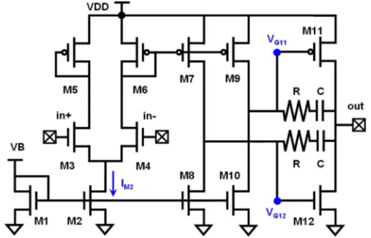
The designed class-B output buffer includes a differential pair stage (M2–M6), a slew-rate enhancement stage (M7–M8 and M9–M10), and a push-pull output stage (M11–M12), as shown in Fig. 3. In this work, this output buffer is connected in unity-gain configuration. The output node (out) is connected to the inverting input node (in-), and the input signal is applied to the non-inverting input node (in+). At stable state, the output voltage should equal to the input voltage. Such unity-gain output buffer is used to drive the large capacitive loading of the data line on LCD panel under gray level transmission.
The diode-connected current source M1 biases all stages in this class-B output buffer. The voltage gain of the differential pair stage is about . The device dimensions of M5, M6, M7, and M9 are drawn the same. The currents flowing through M3–M10 are mirrored from the half current flowing through M2 . The device dimension of M8 is chosen to be a little larger than the half device dimension of M2, but that of M10 is chosen to be a little smaller than the half device di-mension of M2, as shown in the following formulas:
(2) (3) At stable state, the current flowing through M10
is a little less than the half current flowing through M2 due to the designed device dimension . The gate voltage of M12 will be forced to near GND. Sim-ilarly, the gate voltage of M11 is forced to near VDD.
KER et al.: ON-PANEL OUTPUT BUFFER WITH OFFSET COMPENSATION TECHNIQUE 155
Fig. 2. Differential pair circuit (a) with device mismatch. (b) Corresponding to input-referred offset voltages to the output node.
The push-pull output stage is turned off at stable state. When the voltage of the in+ node is increased by , the current flowing through M3 and M5 is increased of , but that through M4 and M6 is decreased of . Therefore, the current flowing through M7 and M9 can be mir-rored by . If the is larger then the , the will be decreased from VDD to turn on M11 and to quickly charge the output node until the voltage of output node and in- node equals to the voltage of the in+ node at stable state. Since M11 and M12 are almost “off” at stable state, this output buffer can drive data line at high frequency with low power consumption on LCD panel.
Fig. 4 shows the measured waveforms of the class-B output buffer connected in unity-gain configuration. The VB is set 1 V on M1 for providing M2, M8, and M10 with constant currents. The total power consumption of this class-B output buffer is about 6.7 mW under 10-V VDD, except the constant current source M1. The class-B output buffer can be operated with the input signals at least 1 MHz, and it has an offset voltage about
Fig. 3. Designed class-B output buffer. (Color version available online at http:// ieeexplore.ieee.org.)
Fig. 4. Measured waveforms of the class-B output buffer in unity-gain connec-tion under 1-MHz sine wave with a 5-V common-mode input voltage. (Color version available online at http://ieeexplore.ieee.org.)
220 mV under a 5-V common-mode input voltage, as shown in Fig. 4.
C. Output Buffer With Offset Compensation
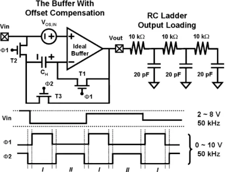
Fig. 5 shows the class-B output buffer with offset compensa-tion circuit used to reduce the offset voltage. The output buffer with offset voltage can be represented as an ideal output buffer without device mismatch and an input-referred offset source. The output node of this unity-gain buffer is connected to an RC ladder output loading for modeling the driving condition on the data line of LCD panel [14]. The input signal has a 2–8-V swing, which indicates different gray levels to drive liquid crystal in unit pixel. The operation frequency of the input signal is defined as the frequency of every datum transferring into the output buffer. The typical operation frequency of the input signal for XGA application is 50 kHz.
The offset compensation circuit contains three switch tran-sistors (T1, T2, and T3) and one offset-holding capacitor . Two complementary clock signals, and , with the
full-Fig. 5. Circuit and the signal-timing diagram of the proposed class-B output buffer with offset compensation circuit to drive an RC ladder output loading.
swing amplitude of 0 V to 10 V and the frequency of 50 kHz are used to control the gate nodes of T1, T2, and T3. Besides, the duty cycle of is set 49% to have a 100-ns nonoverlapping period relative to . Therefore, three switch transistors are un-able to be simultaneously turned on during the signals transient period. The and can be realized on LCD panel by using a two-phase nonoverlapping clock generator [15], but they are temporarily generated by the external source in this work.
The operation sequence of the proposed offset compensation circuit is described in the following. During the period I, the voltage level of is set 10 V to turn on T1 and T2, and the voltage level of is set 0 V to turn off T3. The offset voltage of the output buffer, which is the voltage difference between the output and input signals , can be detected by the paths through T1 and T2. Then, the offset voltage is stored in during the period I. During the period II, the voltage levels of and are 0 and 10 V, respectively. The paths through T1 and T2 connected to are open-circuited, but the path through T3 and con-nected to the inverting input node is short-circuited. Therefore, the detected offset voltage during the period I stored in is added into the inverting input node during the period II. Here, the output voltage in the period II can be expressed as
(4) where is the offset voltage of the output buffer detected during the period II. and can be canceled by each other because almost remains a constant under the same input voltages during these two pe-riods. Therefore, the output voltage can be approached to the input voltage as identical as possible.
Fig. 6 shows the simulated waveforms of the proposed class-B output buffer with offset compensation circuit by using the SmartSpice simulator. One of the input LTPS n-type TFTs
Fig. 6. The simulated output waveform of the proposed class-B output buffers with offset compensation circuit to drive an RC ladder output loading under 50-kHz square input wave with a swing of 2 to 8 V. (Color version available online at http://ieeexplore.ieee.org.)
is set with a large shift of 0.6 V opposite to the others with original value of 1.1 V in this simulation. The input node of this proposed output buffer is applied with a 2–8-V square wave at an operation frequency of 50 kHz. Two complementary signals, and , with a 50-kHz frequency are applied to the gate nodes of three switch transistors. In the period I duration, an 8-V signal is applied on input node, and then the output node presents an offset voltage . However, in the period II duration, the offset voltage of this proposed output buffer can be almost compensated . Therefore, the offset compensation circuit in the unity-gain output buffer can cancel the offset voltage during these two durations.
III. EXPERIMENTALRESULTS
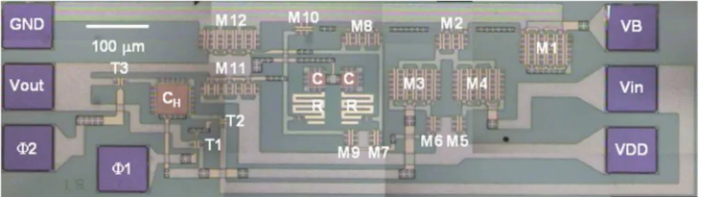
The proposed class-B output buffer with offset compensation circuit has been fabricated in a 3- m LTPS technology. Fig. 7 exhibits the photograph of this fabricated output buffer on glass substrate. The RC ladder output loading is fabricated on panel
KER et al.: ON-PANEL OUTPUT BUFFER WITH OFFSET COMPENSATION TECHNIQUE 157
Fig. 7. Photograph of the fabricated class-B output buffer with offset compensation circuit on panel. (Color version available online at http://ieeexplore.ieee.org.)
Fig. 8. Measured results of the class-B output buffers (a) without and (b) with the offset compensation circuit to drive an RC ladder output loading under 50-kHz square wave with a swing of 2 to 8 V. (Color version available online at http://ieeexplore.ieee.org.)
and connected to the output pad. , , and signals are applied on seven pads of the test output buffer. The total area of this proposed output buffer, including input/output pads, is about m . The VDD and VB are, respectively, set to 10 and 1 V by the power supply. Two
Fig. 9. Offset voltages of the class-B output buffers without and with offset compensation circuit to drive an RC ladder output loading under different input signal levels. (Color version available online at http://ieeexplore.ieee.org.)
Fig. 10. Variation on offset voltages of the class-B output buffers without and with offset compensation circuit to drive an RC ladder output loading in different locations on LCD panel. (Color version available online at http://ieeexplore. ieee.org.)
complementary clock signals, and , are generated by the pulse generator HP8110A. The 2-to-8 V input signal is given by the signal generator HP8116A. All results are measured directly on panel by using probe station in this work.
The functions of the class-B output buffers without and with the offset compensation circuit are verified from the measured waveforms, as shown in Fig. 8(a) and (b), respectively. The class-B output buffer without offset compensation circuit has
stable offset voltage can be measured. When a 5-V signal is ap-plied on the input pad, the offset voltage of the class-B output buffer with (without) offset compensation circuit is about 0 V ( 200 mV). The higher input voltage results in a higher offset voltage of output buffer because the transconductance of TFT at the noninverting input node is increased. By the way, the slope of offset voltage of the output buffer without offset compensation circuit is twice higher than that with an offset compensation cir-cuit. Fig. 10 shows the variation on offset voltages of the class-B output buffers without and with offset compensation circuit in dif-ferent locations on LCD panel. Twenty five class-B output buffers are measured. The variations on offset voltages of the class-B output buffers without and with offset compensation circuit under a 5-V input voltage in different locations on LCD panel are about 100 and 75 mV, respectively (25% reduced). Therefore, the offset compensation circuit can successfully reduce the offset voltage and the variation of the output buffer on LCD panel.
IV. CONCLUSION
A class-B output buffer with offset compensation circuit has been proposed and verified in 3- m LTPS technology. By using the offset compensation technique, the offset voltage of the output buffer can be detected during the first period, and it can be canceled during the next period. The offset voltage can be controlled within 100 mV under input voltage from 2 to 8 V on LCD panel. The variation on offset voltages of the output buffers under different input voltages in different locations has been reduced 25%. The proposed class-B output buffer with offset compensation circuit can be used for the on-panel data driver to provide a high resolution and uniform brightness display.
ACKNOWLEDGMENT
The authors would, especially, like to thank Dr. C.-W. Lin and Dr. Y.-M. Tasi for their help on fabrication of the on-panel circuit in LTPS process.
REFERENCES
[1] K. Chung, M.-P. Hong, C.-W. Kim, and I. Kang, “Needs and solu-tions of future flat panel display for information technology industry,” in IEDM Tech. Dig., 2002, pp. 385–388.
[2] K. Yoneda, R. Yokoyama, and T. Yamada, “Development trends of LTPS TFT LCDs for mobile application,” in Symp. VLSI Circuits, Dig. Tech. Papers, 2001, pp. 85–90.
281–283.
[8] H.-J. Chung, S.-W. Lee, and C.-H. Han, “Poly-Si TFT push-pull ana-logue buffer for integrated data drivers of poly-Si TFT-LCDs,” Elec-tron. Lett., vol. 37, no. 17, pp. 1093–1095, Aug. 2001.
[9] C. Yoo, D.-J. Kim, and K.-L. Lee, “Threshold voltage and mobility mismatch compensated analogue buffer for driver-integrated poly-Si TFT LCDs,” Electron. Lett., vol. 41, no. 2, pp. 65–66, Jan. 2005. [10] S. Maeda, S. Maegawa, T. Ipposhi, H. Kuriyama, M. Ashida, Y. Inoue,
H. Miyoshi, and A. Yasuoka, “An analytical method of evaluating vari-ation of the threshold voltage shift caused by the negative-bias temper-ature stress in poly-Si TFTs,” IEEE Trans. Electron Devices, vol. 45, no. 1, pp. 165–172, Jan. 1998.
[11] M.-D. Ker, C.-K. Deng, and J.-L. Huang, “On-panel design technique of threshold voltage compensation for output buffer in LTPS tech-nology,” in SID, Dig. Tech. Papers, 2005, pp. 288–291.
[12] K. Sera, F. Okumara, H. Uchida, S. Itoh, S. Kaneko, and K. Hotta, “High-performance TFTs fabricated by XeCl excimer laser annealing of hydrogenated amorphous-silicon film,” IEEE Trans. Electron De-vices, vol. 36, no. 12, pp. 2868–2872, Dec. 1989.
[13] K. Pangal, J. C. Sturm, and S. Wagner, “Hydrogen plasma-enhanced crystallization of amorphous silicon for low-temperature polycrys-talline silicon TFTs,” in IEDM Tech. Dig., 1998, pp. 261–264. [14] “TFT-LCD Driver IC—Data Book,” Samsung Electronics,, Yongin,
Korea, 1998.
[15] R. Gregorian, Introduction to CMOS OP-AMPS and Comparators. New York: Wiley, 1999.
Ming-Dou Ker (S’92–M’94–SM’97) received the
B.S. degree in electronics engineering and the M.S. and Ph.D. degrees from the Institute of Electronics, National Chiao-Tung University, Hsinchu, Taiwan, R.O.C., in 1986, 1988, and 1993, respectively.
In 1994, he joined the VLSI Design Department of the Computer and Communication Research Labora-tories (CCL), Industrial Technology Research Insti-tute (ITRI), Taiwan, R.O.C., as a Circuit Design En-gineer. In 1998, he was the Department Manager in the VLSI Design Division of CCL/ITRI. Currently, he is a Full Professor in the Department of Electronics Engineering, National Chiao-Tung University. In the field of reliability and quality design for CMOS integrated circuits, he has published over 250 technical papers in international journals and conferences. He has proposed many inventions to improve reli-ability and quality of integrated circuits, which have granted with 103 U.S. patents and 117 R.O.C. (Taiwan) patents. His current research topics include reliability and quality design for nanoelectronics and gigascale systems, high-speed and mixed-voltage I/O interface circuits, especial sensor circuits, and on-glass circuits for system-on-panel applications in TFT LCD display. He had been invited to teach or to consult reliability and quality design for integrated circuits by hundreds of design houses and semiconductor companies in the Sci-ence-Based Industrial Park, Hsinchu, Taiwan; in the Silicon Valley, San Jose, CA; in Singapore; and in the Mainland China.
Dr. Ker has served as member of the Technical Program Committee and Session Chair of numerous international conferences (including IEEE ISCAS, IEEE AP-ASIC, IEEE SOC, IEEE IRPS, IEEE ISQED, IPFA, EOS/ESD Symp., IEEE VLSI-TSA,. . .). He has served as the Chair of RF ESD committee of 2004 International EOS/ESD Symp., the vice-Chair of Latchup committee for 2005 IEEE International Reliability and Physics Symp. (IRPS), and the Chair of TRD track in 2006 IEEE International Symposium on Quality Electronic De-sign (ISQED). He also served as the Technical Program Committee Chair of
KER et al.: ON-PANEL OUTPUT BUFFER WITH OFFSET COMPENSATION TECHNIQUE 159
2002 Taiwan ESD Conference, the General Chair of 2003 Taiwan ESD Confer-ence, the Publication Chair of 2004 IPFA, and the ESD Program Chair of 2004 International Conference on Electromagnetic Applications and Compatibility. He was the Organizer of the Special Session on ESD Protection Design for Na-noelectronics and Gigascale Systems in ISCAS 2005. Now, he also served as Associate Editor of IEEE TRANS. ON VLSI SYSTEMS. He was elected as the President of Taiwan ESD Association in 2001. He has received many research awards from ITRI, National Science Council, National Chiao-Tung University, and the Dragon Thesis Award from Acer Foundation. In 2003, he was selected as one of the Ten Outstanding Young Persons in Taiwan by Junior Chamber In-ternational (JCI). In 2005, one of his patents on ESD protection design has been awarded with the National Invention Award in Taiwan. He has been selected as a Distinguished Lecturer of the IEEE Circuits and Systems (CAS) Society for the years 2006 and 2007.
Chih-Kang Deng (S’02) was born in Taipei, Taiwan,
R.O.C., in 1977. He received the B.S. degree in electronics engineering and the M.S. degrees from the Institute of Electronics, National Chiao-Tung University (NCTU), Hsinchu, Taiwan, R.O.C., in 2000 and 2002, respectively. He is currently working toward the Ph.D. degree in the Institute of Electronics, NCTU.
His research includes ESD protection and analog buffer circuits on LCD panel.
Ju-Lin Huang was born in Taipei, Taiwan, R.O.C.,
in 1979. He received the B.S. degree in electrical engineering, National Central University (NCU), Taoyuan, Taiwan, R.O.C., in 2002, and the M.S. degree from the Institute of Electronics, National Chiao-Tung University (NCTU), Hsinchu, Taiwan, R.O.C., in 2004.
In 2004, he joined Novatek Microelectronics Cor-poration, Hsinchu, Taiwan, R.O.C., as an IC design engineer. His main research includes the driving cir-cuit design in CMOS and LTPS processes.