Numerical and Experimental Analysis of Cu Diffusion
in Plasma-Treated Tungsten Barrier
Kou-Chiang Tsai,aWen-Fa Wu,b,
*
,zJen-Chung Chen,aTe-Jen Pan,aand Chuen-Guang Chaoa
aDepartment of Materials Science and Engineering, National Chiao Tung University, Hsinchu 300, Taiwan bNational Nano Device Laboratories, Hsinchu 300, Taiwan
This work investigates Cu diffusion in sputtered and N2O plasma-treated W films. N2O plasma-treated W barrier has a nanostruc-tured surface layer and shows high thermal stability and the best barrier properties. Also investigated herein are the lattice and grain boundary diffusivities extracted from the Cu penetration depth profiles using the Whipple analysis of grain boundary diffusion and Fick’s second law of diffusion. Analysis indicates that the diffusion models correlate well with experimental results. © 2004 The Electrochemical Society. 关DOI: 10.1149/1.1833631兴 All rights reserved.
Manuscript submitted March 22, 2004; revised manuscript received June 10, 2004. Available electronically December 1, 2004.
As device dimensions decrease toward 180 nm and below, the necessity for interconnections with resistivity as low as possible is pressing. Copper is now being used in advanced metallization tech-nology due to its low resistivity and high electromigration and stress migration resistance. However, Cu can diffuse into and react with Si or dielectric materials during annealing, and create deep trap levels that cause degradation of device performance and reliability.1,2 Therefore, a qualified diffusion barrier inserted between Cu and Si or dielectric materials is necessary for the Cu metallization. Refrac-tory metals and their nitrides are used as diffusion barriers in copper metallization.3-6Among these materials, tungsten nitride 共WN兲 has received the most attention owing to its high thermal stability and excellent chemical mechanical polishing 共CMP兲 process compatibility.7However, resistivity of tungsten nitride film is higher than that of tungsten film. As the technology node moves to 130 nm and below, a barrier layer with low resistivity is necessary to lower the resistance of the total line interconnect and/or via.
Most refractory metal films used as diffusion barriers in Cu met-allization are polycrystalline rather than monocrystalline. Moreover, columnar grain structure is frequently found in sputtered refractory metal and metal nitride films.8-10In general, atomic diffusion along grain boundaries is much faster than in the bulk of grains. Grain boundaries may presumably serve as fast diffusion paths for copper. Coupled lattice and grain boundary diffusion is different from lattice diffusion. Whipple had given formulas for the concentration in a semi-infinite region of low diffusion coefficient bisected by a thin well-diffusing slab.11,12This is of interest in grain boundary diffu-sion.
In this study, a method of forming nitrogen and oxygen incorpo-rated W films with low resistivity was investigated. N2O plasma was
used to post-treat the W diffusion barrier. The effectiveness of as-deposited and N2O plasma treated W films as diffusion barriers
be-tween Cu and Si was evaluated. A composite diffusion barrier was formed after N2O plasma treatment. Cu diffusion in the N2O plasma
treated W barrier was further analyzed by numerical calculation us-ing Whipple’s and Fick’s models.
Experimental
Single crystal,共100兲 orientated silicon wafers were used in this study. Tungsten films of 50 nm were deposited at a power of 1000 W by sputtering. Films were sputtered at room temperature without intentional heating and base pressure was less than 6⫻ 10⫺7Torr. The wafers further received N2O plasma treatment in a
plasma-enhanced chemical vapor deposition共PECVD兲 system after W films were deposited. The power and pressure of N2O plasma treatment
were 200 W and 100 mTorr, respectively. Some wafers were treated
by N2 or NH3 plasma for comparison. For easy identification, the
untreated, N2O, N2, and NH3plasma-treated W films were denoted
as W, W共N2O), W共N2), and W共NH3) barriers in the work. Copper
films, 300 nm thick, were deposited on top of the barrier layers by sputtering. The efficiency of the diffusion barrier was analyzed by the variation of sheet resistance and leakage current densities of junction diodes after thermal stressing in N2ambient at 500–700°C, i.e., 773–973 K, for 30 min. The wafers were administered a local
oxidation of silicon共LOCOS兲 process to define active regions. The active regions were implanted with 5⫻ 1015 As⫹ions/cm2at en-ergy of 60 keV for n⫹-p junction diodes, and dopants were activated by rapid thermal annealing共RTA兲 in N2ambient at 1050°C for 30 s.
Leakage currents of diodes were measured at a reverse bias of 5 V by a HP 4156 semiconductor parameter analyzer. A four-point probe system was employed to measure sheet resistance.
Film thickness was measured by a stylus surface profiler and scanning electron microscopy 共SEM兲. X-ray photoemission spec-troscopy共XPS兲 was used to study the bonding structures and chemi-cal binding energies. The microstructure and grain size of the film were examined using transmission electron microscopy 共TEM兲. Structure and crystalline orientation of as-deposited and annealed samples were analyzed by an X-ray diffractometer共XRD兲 with Cu K␣ radiation operated at 50 kV and 250 mA. Surface roughness and morphology of the film were observed using a Digital Instruments Nanoscope II model atomic microscope共AFM兲 with a 0.5 Hz scan-ning speed in air ambient. Surface morphology was studied by a field-emission scanning electron microscope 共FESEM兲. Composi-tional depth profiles were measured by secondary ion mass spec-trometry共SIMS兲.
Results and Discussion
To investigate the effects of N2O plasma treatment on W barrier,
chemical bonding states of barrier were analyzed by XPS. Figure 1a-c show the W 4f, O 1s, and N 1s spectra of as-deposited and N2O
plasma-treated W barriers. The W 4f7/2and W 4f5/2peaks are
situ-ated at the same position共31.2, 33.4 eV兲 for two barriers, and the two peaks are characteristics of the W itself.13However, two other peaks at binding energies 36.2 and 38.4 eV are observed for the W共N2O) barrier. The peaks correspond to binding energies of
tung-sten oxide and are attributed to oxidation during N2O plasma
treat-ment. The O 1s spectrum of the W共N2O) barrier exhibits a strong
and broad peak centered at around 531.2 eV, as shown in Fig. 1b. There is almost no peak in untreated W barrier. W-O phases are believed to form at the surface of W共N2O) barrier. The N 1s peak of
the W共N2O) barrier can be well resolved into two peaks by curve
fitting compared to no peak in the N 1s spectrum of the W barrier, as shown in Fig. 1c. These two peaks are centered at 397.5 and 399.3 eV. The weak peak centered at 397.5 eV is consistent with the N 1s binding energy of nitride compound and is also reported by previous research.14Another strong peak at⬃399.3 eV is observed in N 1s *Electrochemical Society Active Member.
zE-mail: [email protected]
Journal of The Electrochemical Society, 152共1兲 G83-G91 共2005兲
0013-4651/2004/152共1兲/G83/9/$7.00 © The Electrochemical Society, Inc.
spectrum. This indicates that some N atoms do not form strong covalent or ionic bonds with W during N2O plasma treatment. Some
N atoms or molecules may present in grain boundaries of W.8,15,16 Figure 2a displays cross-sectional bright field TEM micrograph of as-sputtered W film. Columnar grain structure is observed. Cu diffusion in columnar grains is believed to be relatively easy be-cause columnar grains will provide fast diffusion paths for Cu
dif-fusion. Figure 2b and c display plane-view TEM images and se-lected area diffraction共SAD兲 patterns of W and W共N2O) barriers.
Several sharp rings are observed for untreated W film. This indicates that the as-deposited W film is a polycrystalline structure. The grain size of as-deposited W film is 20– 40 nm, as shown in Fig. 2b. The W共N2O) barrier has a diffused ring pattern instead of diffraction
spots, indicating that the N2O plasma treatment causes an
amor-Figure 1.共a兲 W 4f, 共b兲 O 1s, and 共c兲 N 1s XPS spectra of W and W共N2O)
barriers.
Figure 2.共a兲 Cross-sectional bight field TEM image of W barrier. Plane-view TEM images and SAD patterns of the共b兲 W and 共c兲 W共N2O) barriers.
phous surface layer upon W film. Grain size of the W共N2O) barrier
is only 2–5 nm. This indicates that a surface layer with finer grains is formed due to the reactions and bombardments of energetic radi-cals and ions during plasma treatment. It is reported that the nano-structured amorphous diffusion barrier, defined as a very short-range order single crystal, is highly attractive due to its relatively high thermal stability and its relatively higher resistance against Cu diffusion.17
Figure 3 displays resistivity and root-mean-square 共RMS兲 sur-face roughness of plasma treated W film as a function of plasma treatment time. Surface roughness reduces apparently after plasma treatment, as shown in Fig. 3. Plasma treatment could sputter the barriers and make them smooth. Sputtering and stuffing effects are believed to occur due to the reactions or bombardments of energetic radicals and ions during plasma treatment. Resistivity increases with increasing plasma treatment time. It is expected that resistivity of W with plasma treatment would increase because a high-resistivity sur-face layer is formed and thus the effective thickness of the W film with low resistivity reduces. Resistivity of W共N2O) barrier is higher
than those of the W共N2) and W共NH3) barriers. High resistivity may
be due to the formation of high-resistance W-O compounds in W共N2O) barrier, as indicated in XPS analyses. However, the
resis-tivity of W共N2O)共⬃24 ⍀ cm兲 barrier is still much lower than that
of the reactively sputtered WN film (150⬃ 200 ⍀ cm兲.8 Table I summarizes the properties of W, WN and W共N2O)
bar-riers. Table I also lists properties of sputtered Ta and Ti films in literatures4,6,16,18 for comparison. The resistivities of sputtered W and W共N2O) barriers are about 20 and 24O cm, respectively. The
resistivities are very close and much lower than that of the reactively sputtered WN 共150–200 O cm兲,8 Ta 共⬃160 O cm兲,4,16 and Ti 共⬃70 O cm兲.18Hara et al. have reported that the agglomeration
and adhesion strength of the copper seed layer, its crystallographic orientation along共111兲, and the resistivity of the subsequent
electro-plated copper layer, are affected by the stress in the copper seed layer deposited on the barrier layer.19,20Electroplating of Cu layer is difficult on seed layers with rough surface. Surface roughness could be reduced from 2.5 to 0.5 nm by N2O plasma treatment, as listed in
Table I. Grain size is calculated from plane-view TEM. The as-deposited W film is columnar grain structure with a grain size of 20– 40 nm and grain size of the W共N2O) barrier is only 2–5 nm.
This indicates that nanocrystallization effect would occur due to the reactions and bombardments of energetic radicals and ions during N2O plasma treatment. Furthermore, it is reported that the impurities
共nitrogen or oxygen兲 in the films are responsible for the intrinsic compressive stress.21 In this research, the tensile stress decreases from 1.9⫻ 1010to 1.4⫻ 109dynes/cm2as N
2O plasma treatment
is applied to W film, as listed in Table I. N2O plasma treatment also
enhances the adhesion between Cu and W共N2O) barrier. The
adhe-sion strength of Cu on W共N2O) barrier 共50–58 Mdynes/cm2兲 is
Figure 3. Resistivity and RMS surface roughness of W共N2), W共NH3), and
W共N2O) films as a function of plasma treatment time.
Figure 4. 共a兲 Variation percentage in sheet resistance of Cu/barrier/Si as a
function of annealing temperature. 共b兲 XRD spectra of Cu/W/Si and Cu/W共N2O兲/Si contact systems after annealing at 700°C for 30 min.
Table I. Properties of W, WN, and W„N2O… diffusion barriers. Properties of sputtered Ta, Ti films are also listed for comparison. Leakage
current densities of diodes were measured at a reverse bias of 5 V after annealing at 600°C for 30 min.
W W共N2O) WN 8 Ta4,6,16 Ti6,18 Resistivity共O cm兲 ⬃20 ⬃24 150–200 ⬃160 ⬃70 RMS roughness共nm兲 2.5 ⬃0.5 1–2 4 3.2– 4.2 Grain Size共nm兲 20– 40 2–5 5–15 20 10–30 Stress共dynes/cm2兲 1.9⫻ 1010 1.4⫻ 109 1.5⫻ 1010 2.0⫻ 1010 3.9⫻ 109
Adhesion poor good poor poor fair
Leakage current
density共A/cm2兲 ⬃9.0 ⫻ 10
⫺4 ⬃3.0 ⫻ 10⫺9 ⬃8.5 ⫻ 10⫺6 2.5⫻ 10⫺5 5.5⫻ 10⫺4
better than untreated W 共30–35 Mdynes/cm2兲 and other barriers such as Ta and Ti.6It is suggested that O or N species on the barrier surface can react with Cu to form more stable interface and thus promote adhesion after N2O plasma treatment.
Figure 4a shows the variation percentage of the Cu/barrier/Si system after furnace annealing at various temperatures. The varia-tion in sheet resistance is defined as the ratio of (R⫺ R0) to R0, in
which R0 and R denote the sheet resistance of as-deposited and
annealed samples. The results reflect the interactions between Cu and Si indirectly. Resistance increases rapidly at certain temperature because of failure of the diffusion layer and formation of com-pounds. Sheet resistance of Cu/W共N2O兲/Si increases slightly even
after annealing at 750°C. However, sheet resistances of samples with other barriers共W, WN,8WCx,22TiCx,23and TaN24兲 sharply
increase after annealing at 600–700°C, indicating that a consider-able amount of Cu has already diffused through the barrier layers and resulted in Cu3Si compounds, and thus strongly deteriorated the
conductivity of the contact system. XRD was further used to detect the structural change in the annealed samples. Figure 4b shows XRD patterns of Cu/W/Si and Cu/W共N2O兲/Si systems after
anneal-ing at 700°C for 30 min. Peaks of Cu3Si compounds are observed
for W barrier and the resulting XRD pattern is consistent with varia-tion in sheet resistance. There is no Cu3Si peak in W共N2O) barrier
system, indicating that W共N2O) has an excellent barrier
perfor-mance. It is noted that there is no Cu-W compound in the XRD spectra, and similar results are found for WN barriers.8The failure of W and WN barriers is attributed that Cu atoms diffuse through defects and grain boundaries of the barrier without reacting with the
WN and W film. Failure temperature 共variation percentage ⬎ 50%) of W共N2O) barrier is higher than 750°C and superiors to
sputtered WCx(⬃650°C),22TiCx(⬃625°C),23and TaN共⬃650°C兲24
barriers.
Barrier performance is also evaluated by the leakage current den-sity of the junction diode. Figure 5 illustrates the statistical distribu-tions of leakage current densities of Cu/barrier/n⫹-p junction diodes measured at reverse bias of 5 V after annealing at 500 and 600°C. The leakage current densities of all diodes are below 10⫺8 A/cm2 before annealing. Most diodes with sputtered W, WN,8WCx,22and
TiCx23 barriers have leakage current densities higher than 1
⫻ 10⫺7 A/cm2after annealing at 500°C for 30 min. Diodes with
W共N2O) barriers retain leakage current densities less than 10⫺8
A/cm2 after annealing at 500°C. Moreover, most diodes with W共N2O) barriers retain leakage current densities less than 10⫺8
A/cm2even after annealing at 600°C. W共N2O) show an excellent
barrier capability against Cu diffusion compared to W, WN,8 WCx,22TiCx,23and TaN,24as shown in Fig. 5.
Although barrier performance of the W film is significantly im-proved by N2O plasma treatment, similar plasma treatments, e.g.,
N2 plasma treatment, had been proposed to enhance barrier
perfor-mance in previous researches.15,16W barriers are also treated by N2
or NH3plasma for comparison in the work. Figure 6 exhibits
statis-tical distributions of leakage current densities of Cu/W共N2O兲/n⫹-p,
Cu/W共N2)/n⫹-p and Cu/W共NH3)/n⫹-p diodes after annealing at
500 and 600°C. All W共N2O), W共N2), and W共NH3) show an
en-hanced barrier performance compared to untreated W. Moreover, N2O plasma treatment has a better barrier improvement than N2 Figure 5. Statistical distributions of leakage current densities of copper
con-tacted n⫹-p junction diodes with various diffusion barriers after annealing at 共a兲 500 and 共b兲 600°C for 30 min.
Figure 6. Statistical distributions of leakage current densities of copper
con-tacted n⫹-p junction diodes with various plasma-treated W diffusion barriers after annealing at共a兲 500 and 共b兲 600°C for 30 min.
plasma treatment and N2plasma is more effective than NH3plasma.
It is found that some diodes have leakage current densities higher than 1⫻ 10⫺7 A/cm2 for W共NH3) barriers after annealing at
500°C. Most diodes with W共N2O) barriers retain leakage current
densities less than 1⫻ 10⫺8A/cm2and large leakage current den-sities in range of 10⫺7 to 10⫺4 are found for Cu/W共N2)/n⫹-p and
Cu/W共NH3)/n⫹-p diodes after annealing at 600°C. Enhancing
per-formance of the W共N2O) barrier is attributed to combined effects of
nitridation and oxidation during N2O plasma treatment. N2O is a
strong oxidizing agent and energetic oxygen radicals and atoms are more easily produced by dissociation of N2O. In contrast, it is less
effective to dissociate triple bonds of nitrogen as nitrogen plasma is used to post-treat W barrier. The bond strengths of N-O and N-N are 630.57 and 945.33 kJ/mol. Energetic oxygen radicals and atoms are helpful in formation of an oxygen stuffed layer on the columnar-grained W barrier. It will act as a more efficient barrier against the Cu diffusion. N2plasma treatment does not induce oxygen stuffed
layer on surface of the W barrier and nitrogen radicals and atoms are limited for nitridation and stuffing compared to N2O plasma
treat-ment. Bond strength of N-H is 339 kJ/mol for NH3 plasma
treat-ment. Although nitridation is expected to occur greatly, no plasma oxidation on W surface occurs and lots of atomic hydrogen will diffuse into the grain boundaries of W due to effective dissociation of NH3. Hydrogen will out-diffuse from grain boundaries of
plasma-treated W after annealing at a certain temperature, lead to defect sites or carrier trapping sites, and hence, decrease its resis-tance to copper penetration.
Barrier capabilities are further investigated by evaluating Cu dif-fusion in W and W共N2O) barriers. The diffusion of Cu in the
tem-perature range of 600–700°C is evaluated by SIMS and the penetra-tion depth profiles of specimens are indicated in Fig. 7. Relatively low Cu penetration into the W共N2O) barrier is detected compared to
sputtered W barrier. Because the mixing enthalpy of Cu solute in W is large (8.0⫻ 104j/mol兲, Cu atoms do not intermix with W at high
temperature.25,26As far as we know, it is relatively difficult for Cu penetration into W barrier by lattice diffusion. However, the diffu-sion coefficients of Cu in grain boundaries of W barrier are still Figure 7. SIMS distribution profiles of the copper elements in共a兲 Cu/W/Si
and共b兲 Cu/W共N2O兲/Si after annealing at 600, 650, and 700°C in N2ambient
for 30 min.
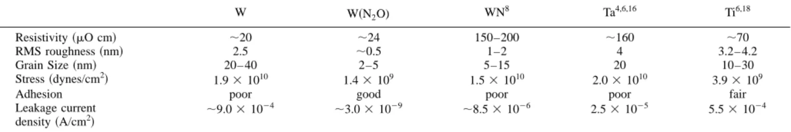
Figure 8. Penetration plots for Cu diffusion into W films at various
tempera-tures of共a兲 600, 共b兲 650, and 共c兲 700°C. The solid curve is the fitting curve.
DB␦ ⫽ 0.661
冉
⫺ ln共C¯兲 y6/5冊
⫺5/3冉
4DL t冊
1/2 关1兴 where C¯ ⫽ C/Cs, C represents the concentration in a section at a depth ym from the original surface, Csis the surfaceconcentra-tion, t is the annealing time, and d is the grain boundary width. DL
and DBpresent the diffusion coefficients in the lattice and the grain
boundary. Figure 8 displays the concentration profiles obtained from diffusion of Cu in W barriers at various temperatures in the standard coordinates ln C¯ vs. y6/5. Based on Eq. 1 and provided that DLis
known,␦DB can be determined by measuring the slope from the
linear region in the ln C¯ vs. y6/5plots. The value of DLcan be found
from the initial part of the concentration profile. Under the assump-tions of a semi-infinite system and constant source at the surface, the boundary conditions applied to solve Fick’s diffusion equation are
C⫽ Cs, y ⬍ 0, t ⫽ 0 关2兴
C⫽ 0, y ⬎ 0, t ⫽ 0 关3兴
An error function solution can be expressed by the equation
C共y, t兲 ⫽ Cserfc
冉
y2
冑
DLt冊
关4兴where the error function was fitted to the initial part of the concen-tration profiles and extrapolated to zero thickness y⫽ 0 in the case of subtracting the grain boundary contribution. The results are shown in Table II, and the derived value of DLwas used to calculate
␦DB. To obtain a value DB, a grain boundary width must be
as-sumed, it is reasonable to assume a width of about two atom layers, ␦ ⫽ 5 ⫻ 10⫺8 cm.28,29
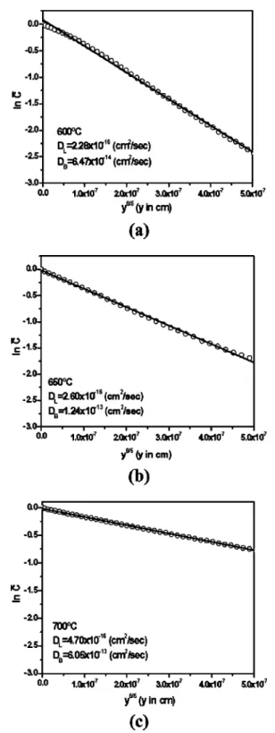
pendence of the lattice diffusivity in W barrier can be expressed by the Arrhenius relation of DL⫽ DL0exp(⫺QL/kT), where DL0 and QLare pre-exponential factor and activation energy for lattice dif-fusion. The dependency is plotted in Fig. 10. The values of diffu-sivities, pre-exponential factors, and activation energies are summa-rized in Table II. The D values of Cu in sputtered W films are smaller than those in CVD-W films, but the magnitudes are in the same order. In addition, the activation energy of Cu diffusion in sputtered W films is somewhat larger than that in CVD-W films.27,30 Similar numerical analysis can be applied to evaluate the effects of Cu diffusion in W共N2O) barriers. As mentioned previously, N2O
plasma treatment causes an amorphous surface layer upon the W film. This is the case of a semi-infinite medium which has a skin or surface layer W共N2O)1 having diffusion properties different from
those of the rest of the medium W共N2O)2. The subscripts 1 and 2
denote the amorphous surface layer and the rest in the W共N2O)
barrier. Thus, suppose in the semi-infinite region⫺h ⬍ y⬘⬍ ⬁, the lattice diffusion coefficient is DL1in the region⫺h ⬍ y⬘⬍ 0, and
the concentration is denoted by C1 there, while the corresponding
quantities in y⬘⬎ 0 are DL2and C2. Assume the conditions at the
interface to be C1⫽ C2, y⬘⫽ 0 and DL1C1/y⬘
⫽ DL2C2/y⬘, y⬘⫽ 0 the solution to the problem of zero initial
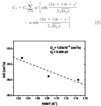
concentration and the surface y⬘⫽ ⫺h maintained at constant con-centration C0is given as12 C1⫽ C0
兺
n⫽0 ⬁ ␣n再
erfc共2n ⫹ 1兲h ⫹ y⬘ 2冑
DL1t ⫺ ␣ erfc共2n ⫹ 1兲h ⫺ y⬘ 2冑
DL1t冎
关5兴Figure 9. The Arrhenius plot of the grain boundary diffusivity DBfor Cu
diffusion in W films.
Figure 10. The Arrhenius plot of the lattice diffusivity DLfor Cu diffusion
C2⫽ 2kC0 k ⫹ 1
兺
n⫽0 ⬁ ␣nerfc共2n ⫹ 1兲h ⫹ ky⬘ 2冑
DL1t 关6兴 where k⫽冑
DL1/DL2, ␣ ⫽ (1 ⫺ k)/(1 ⫹ k)The thickness h of the surface layer W共N2O)1 is about 3 nm
from high-resolution TEM micrograph. Both diffusion coefficients can be obtained by numerical calculation. The values of DL1 and DL2can be roughly estimated from fitting of experimental concen-tration profiles using an error function solution such as that in Eq. 4. The estimated values are used as the initial guess of DL1 and DL2
and further substituted into the Eq. 5 and 6 to obtain concentrations
C1 and C2, respectively. To quickly obtain the numerical
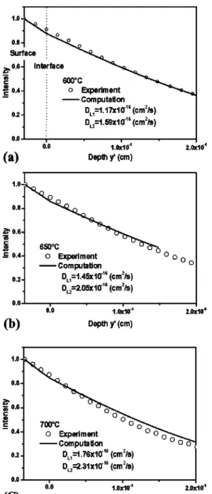
conver-gence, the high order terms are neglected in the Eq. 5 and 6 during the calculation. It is found that the calculated error is smaller than 10⫺4 as n⫽ 4. The asymptotic solutions of lattice diffusion coeffi-cients can be obtained by steep-descent method and fitting of the experimental concentration profile. Figure 11 shows experimental and calculated concentration profiles. The derived values of DL1and DL2are listed in Table III.
Similarly, grain boundary diffusion coefficients DB2in W共N2O)2
region can be determined from the derived lattice diffusion coeffi-cient DL2 and the slope in ln C¯ vs. y⬘6/5 plots. Figure 12 displays
experimental concentration profiles for Cu diffusion in W共N2O)
bar-riers at various annealing temperatures in the standard coordinates ln C¯ vs. y⬘6/5. The derived grain boundary diffusion coefficients D
B2
are listed in Table III. Table III summaries the values of diffusion coefficients and pre-exponential factors for Cu diffusion in W共N2O)
barriers. Other barrier materials in literatures are also listed for comparison.27,30,31 The W共N2O) barrier shows small lattice
diffu-sion coefficients compared to W2N, W, and TiB2barriers. The
varia-tion of DL2with temperature is slight for the W共N2O) barrier,
indi-cating that the W共N2O) barrier has better thermal stability.
One significant finding in the present study is that some atomic nitrogen and oxygen will react with W, segregate at grain boundaries of W film as impurities, and act as a stuffing agent to block fast diffusion path during N2O plasma treatment. Nitrogen addition will
stuff the grain boundaries of W and nitrify tungsten to form tungsten nitride, as shown in XPS analyses of Fig. 1c. Similar nitridation effect had been reported by Hara et al.32A TiN barrier was formed at the surface of the Ti layer in high-pressure ammonium ambient. Figure 13 shows cross sections of the interfacial structures of Cu/ W/Si and Cu/W共N2O兲/Si samples before and after annealing. The
as-deposited W barrier has a columnar grain structure as shown in Fig. 13a. The failure of W barrier is attributed to the Cu diffusion through the columnar W to form Cu3Si after annealing at 700°C for
30 min. Grain boundary diffusion coefficients are 6.5⫻ 10⫺14 ⬃ 6.1 ⫻ 10⫺13 cm2/s using Whipple analysis of grain boundary
Figure 11. Penetration plots for Cu diffusion into W共N2O) films at various
temperatures of共a兲 600, 共b兲 650, and 共c兲 700°C. The solid curve is the profile calculated from Eq. 5 and 6.
Table III. Summary of the values of diffusivities, and pre-exponential factors for Cu diffusion in W„N2O… films and at various annealing
temperatures. Other barrier materials are also listed for comparison.
Sample T共°C兲 DL共cm 2 /s兲 DB共cm 2 /s兲 DL0共cm 2 /s兲 DB0共cm2/s兲 DL1 DL2 DB2 DL0,1 DL0,2 W共N2O) 600 1.17⫻ 10⫺16 1.58⫻ 10⫺16 4.07 ⫻ 10⫺14 6.12⫻ 10⫺15 6.43⫻ 10⫺15 9.28⫻ 10⫺13 650 1.45⫻ 10⫺16 2.04⫻ 10⫺16 5.37 ⫻ 10⫺14 700 1.76⫻ 10⫺16 2.31⫻ 10⫺16 5.57 ⫻ 10⫺14 W2N27 600 1.15⫻ 10⫺16 7.00⫻ 10⫺11 700 4.52⫻ 10⫺16 W30 600 2.4⫻ 10⫺16 1.11⫻ 10⫺13 700 4.5⫻ 10⫺16 TiB231 500 1.4⫻ 10⫺15 600 2.0⫻ 10⫺15 700 5.3⫻ 10⫺15 800 5.0⫻ 10⫺14
diffusion. The barrier capability of the W film against Cu diffusion can be improved by N2O plasma treatment. An oxidation and
nitridation layer with nanostructured grains is formed on the surface of the stuffed W barrier, as shown in Fig. 13b. Relatively low dif-fusion coefficients are found. No Cu silicide compound is observed for Cu/W共N2O兲/Si sample after annealing at 700°C for 30 min
be-cause nanostructured and stuffed barrier can effectively impede Cu diffusion.
Conclusion
The effectiveness of W共N2O) films as diffusion barriers between
Cu and Si has been investigated. W共N2O) films, which have
amor-phous and nano-grained surface layers, show high thermal stability, low resistivity, low surface roughness, low tensile stress, and better adhesion with Cu. W共N2O) barriers show excellent barrier
capabili-ties against Cu diffusion. Cu/W共N2O兲/n⫹-p junction diodes retain
leakage current densities less than 10⫺8A/cm2even after annealing at 600°C. Copper diffusion in W and W共N2O) barriers is further
analyzed using the Whipple analysis of grain boundary diffusion and Fick’s diffusion law. Both lattice and grain boundary diffusivities of Cu diffusion in W and W共N2O) barriers are extracted from the Cu
concentration profiles after annealing the samples at 600–700°C. Grain boundary diffusion coefficients of Cu in sputtered W films are 6.5⫻ 10⫺14⬃ 6.1 ⫻ 10⫺13cm2/s. Relatively low diffusion coeffi-cients are found in W共N2O) barriers because oxidation and
nitrida-tion layers with nano grains are formed at the surface of the stuffed W barriers after N2O plasma treatments.
Acknowledgments
The work reported was financially supported by the National Science Council of the Republic of China under contract no. NSC 92-2215-E-492-002 and supported, in part, by the Ministry of Eco-nomic Affairs of the Republic of China under contract no. 92-EC-17-A-08-S1-0003. Technical support from the National Nano De-vice Laboratories is greatly acknowledged.
The National Nano Device Laboratories assisted in meeting the publica-tion costs of this article.
References
1. S. D. Brotherton, J. R. Ayres, A. Gill, H. W. V. Kesteren, and F. J. A. M. Greidanus,
J. Appl. Phys., 62, 1826共1987兲.
2. J. M. Shieh, K. C. Tsai, and B. T. Dai, Appl. Phys. Lett., 82, 1914共2003兲. 3. S. M. Rossnagel, I. C. Noyan, and C. Cabral, Jr., J. Vac. Sci. Technol. B, 20, 2047
共2002兲.
4. W. L. Yang, W. F. Wu, D. G. Lin, C. C. Wu, and K. L. Ou, Solid-State Electron., 45, 149共2001兲.
5. K. H. Min, K. C. Chun, and K. B. Kim, J. Vac. Sci. Technol. B, 14, 3263共1996兲. 6. H. Ono, T. Nakano, and T. Ohta, Appl. Phys. Lett., 64, 1511共1994兲.
7. S. Wong, C. Ryu, H. Lee, and K. Kwon, Mater. Res. Soc. Symp. Proc., 514, 75 共1998兲.
8. K. C. Tsai, W. F. Wu, J. C. Chen, T. J. Pan, and C. G. Chao, J. Vac. Sci. Technol.
B, 22, 993共2004兲.
9. W. F. Wu, K. C. Tsai, C. G. Chao, C. F. Huang, S. T. Wu, Y. L. Chin, and B. S. Chiou, in Proceedings of the 17th International VLSI Multilevel Interconnection
Conference, IEEE, p. 490共2000兲.
10. J. C. Lin and C. Lee, J. Electrochem. Soc., 146, 3466共1999兲. 11. R. T. P. Whipple, Philos. Mag., 45, 1225共1954兲.
Figure 12. Penetration plots for Cu diffusion into W共N2O) films at various
temperatures of共a兲 600, 共b兲 650, and 共c兲 700°C. The solid curve is the fitting curve.
Figure 13. Schematic illustrations of the microstructures of共a兲 Cu/W/Si and
12. J. Crank, The Mathematics of Diffusion, Clarendon Press, Oxford共1975兲. 13. J. F. Moulder, W. F. Stickle, P. E. Sobol, and K. D. Bomben, Handbook of X-Ray
Photoelectron Spectroscopy, Physical Electronics, Inc., Eden Prairie, MN共1995兲.
14. T. Nakajima, K. Watanabe, and N. Watanabe, J. Electrochem. Soc., 134, 3175 共1987兲.
15. K. M. Chang, T. H. Yeh, I. C. Deng, and C. W. Shih, J. Appl. Phys., 82, 1469 共1997兲.
16. W. F. Wu, K. L. Ou, C. P. Chou, and C. C. Wu, J. Electrochem. Soc., 150, G83 共2003兲.
17. D. J. Kim, Y. T. Kim, and J. W. Park, J. Appl. Phys., 82, 4847共1997兲. 18. M. E. Day, M. Delfino, J. A. Fair, and W. Tsai, Thin Solid Films, 254, 285共1995兲. 19. T. Hara, Y. Yoshida, and H. Toida, Electrochem. Solid-State Lett., 5, G36共2002兲. 20. T. Hara, Y. Shimura, and H. Toida, Electrochem. Solid-State Lett., 6, C97共2003兲. 21. H. Windischmann, J. Vac. Sci. Technol. A, 9, 2459共1991兲.
22. S. J. Wang, H. Y. Tsai, S. C. Sun, and M. H. Shiao, J. Electrochem. Soc., 148, G500 共2001兲.
23. S. J. Wang, H. Y. Tsai, S. C. Sun, and M. H. Shiao, J. Electrochem. Soc., 148, C563 共2001兲.
24. M. H. Tsai, S. C. Sun, C. E. Tsai, S. H. Chuang, and H. T. Chiu, J. Appl. Phys., 79, 6932共1996兲.
25. M. E. Glicksman, Diffusion in Solid, p. 207, Wiley Interscience, New York共2000兲. 26. F. R. de Boer, R. Boom, W. C. M. Mattens, A. R. Miedema, and A. K. Niessen,
Cohesion in Metals, Transition Metal Alloys, North-Holland, Amsterdam共1988兲.
27. M. Uekubo, T. Oku, K. Nii, M. Murakami, K. Takahiro, S. Yamaguchi, T. Nakano, and T. Ohta, Thin Solid Films, 286, 170共1996兲.
28. D. Gupta and T. T. C. Tsui, Appl. Phys. Lett., 17, 294共1970兲. 29. J. C. Fisher, J. Appl. Phys., 22, 74共1951兲.
30. K. Vieregge and D. Gupta, Tungsten and Tungsten Alloys-Recent Advances, p. 231, The Minerals, Metals and Materials Society共1991兲.
31. J. Pelleg and G. Sade, J. Appl. Phys., 91, 6099共2002兲.
32. T. Hara, K. Tani, and K. Inoue, Appl. Phys. Lett., 57, 1660共1990兲.