IEEE ELECTRON DEVICE LETTERS, VOL. 31, NO. 2, FEBRUARY 2010 135
Pentacene-Based Organic Phototransistor With High
Sensitivity to Weak Light and Wide Dynamic Range
Hsiao-Wen Zan, Member, IEEE, Shih-Chin Kao, and Shiang-Ruei Ouyang
Abstract—In this letter, the channel length effect, combined with
the photoelectric field effect of organic phototransistors, has been investigated for the first time. Reducing the channel length and applying a positive gate bias during illumination enhance electron trapping effectively and hence improve the photoresponsivity of a pentacene-based phototransistor. The sensing dynamic range and the photosensitivity to very weak light (in the range of microwatts per square centimeter) are also discussed through the interaction between deep trapped states, interface energy-band bending, and photoexcited electrons.
Index Terms—Channel length, pentacene, photoresponsivity,
phototransistor, thin-film transistor (TFT). I. INTRODUCTION
O
RGANIC thin-film transistors (OTFTs) have attracted much attention because of their low-temperature process-ing, flexibility, and lightweight [1], [2]. Aside from serving as a switch in display, an OTFT exhibits high photoresponsivity (Rph) and can be used as an organic phototransistor (OPT) [3]– [5]. Under illumination, excitons generated in a pentacene film dissociate into electrons and holes. Holes can be well conducted without being significantly trapped. Light-induced electrons, on the contrary, are easily trapped by deep electron-trapping states in a pentacene film [6]. When electrons are trapped close to the organic/dielectric interface, OPT exhibits pronounced light-induced threshold-voltage shift (ΔVTHLight) [3], [7]. ΔVTHLight increases the photocurrent at a fixed gate bias and thus enhancesRph. Recently, many reports found that the Rph or ΔVTHLight of OPT can be significantly enlarged by applying an electric field during light irradiation (named as photoelectric field effect in this letter) [4], [7]. However, the influences of electric field and channel length on electron trapping have not been studied under illumination. When OPT is used to detect light signals with various intensities, the dynamic detecting range is not also investigated. In this letter, pentacene-based OPTs with different channel lengths are used to detect light signals with various intensities. The electric field effect, channel length effect, and dynamic detecting range under repeated operation are discussed.
II. EXPERIMENTALSETUP
Conventional top-contact pentacene-based TFTs were used. Spinning poly(methyl methacrylate) (PMMA) onto SiO2serves
Manuscript received October 1, 2009; revised November 15, 2009. First published January 19, 2010; current version published January 27, 2010. This work was supported by the National Science Council (NSC-98-2627-B009-008). The review of this letter was arranged by Editor P. K.-L. Yu.
The authors are with the Department of Photonics and the Institute of Electro-Optical Engineering, National Chiao Tung University, Hsinchu 300, Taiwan (e-mail: [email protected]).
Digital Object Identifier 10.1109/LED.2009.2037591
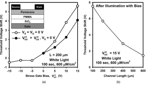
as a dual-layer gate dielectric. The inset of Fig. 1(a) shows the device geometry. The thickness of both SiO2 and PMMA layers is 100 nm. Unpurified pentacene obtained from Aldrich was evaporated through a shadow mask onto the PMMA layer. The deposition rate was set at 0.5 Å/s, while the substrate was kept at room temperature. After the formation of 100-nm-thick pentacene, 100-nm-100-nm-thick gold was deposited through the shadow mask to form source/drain contacts. The device channel length (L) varied from 100 to 600 μm, while the channel width (W ) was fixed at 1000 μm.
A white-light-emitting diode (LED) was used as backlight to irradiate the sample from the top. The device was measured at room temperature and in ambient air. The threshold voltage was extracted using the linear region equation [8].
III. RESULTS ANDDISCUSSION
Before stress or irradiation, devices exhibit a field-effect mo-bility and a threshold voltage of 0.36 cm2/V· s and −14.5 V,
respectively. The subthreshold slope is 0.9 V/decade for devices with channel lengths varying from 200 to 600 μm and is 2.7 V/decade for devices with channel lengths of 100 μm. First, (ΔVTHLight) is investigated using bias stress to control the light-induced threshold voltage shift. ΔVTHLight is defined as
Vth–Vthini, where Vthiniand Vthare threshold voltages under illu-mination before and after bias stress. The white-light source is used to illuminate the device (W/L = 1000 μm/200 μm) with an intensity of 600 μW/cm2 for 100 s. During illumination, bias stress is also applied using different stressed gate biases (Vst
GS’s). The stressed drain bias (VDSst) is 0 V or equal to VGSst. The source electrode is grounded. Before and after the 100-s illumination with different stress conditions, transfer character-istics are measured promptly under illumination. Then, ΔVTHLight is shown as a function of Vst
GSin Fig. 1(a). White circles repre-sent ΔVTHLightfor the grounded drain, while black circles repre-sent ΔVTHLightfor VDSst = VGSst. When VGSst = 0 V, ΔVTHLightis a small positive value because of electron trapping. When a nega-tive gate bias is applied during illumination, ΔVTHLightshifts to become negative owing to the compensation between the light-induced electron trapping and the bias-light-induced hole trapping. Applying a positive gate bias obviously enhances ΔVTHLight ow-ing to electron trappow-ing. Effective electron trappow-ing results from the separation of light-generated excitons and the equilibrium of trapping and recombination. The separation of excitons can be enhanced by an electric field through field-induced dissociation [4], [6], [7]. In our study, the electric field across the channel film close to the source/drain electrodes (vertical field) is usually much higher than the electric field along the channel length from the source to drain electrodes (lateral
136 IEEE ELECTRON DEVICE LETTERS, VOL. 31, NO. 2, FEBRUARY 2010
Fig. 1. (a) Light-induced threshold-voltage shift ΔVTHLightas a function of gate bias. The bias conditions are as follows: VD= VS= 0 V and VDSst = VGSst, VS= 0 V. (b) Light-induced threshold-voltage shift ΔVTHLightas a function of channel length.
Fig. 2. (a) ΔVTHLightas a function of light intensity under various gate biases. (b) Energy-band diagram of OPT from the gate to the drain/source when devices are under illumination with a positive gate bias.
field). A high vertical field (higher than 2× 10⁴V/cm [9]) may be effective in dissociating excitons. Additionally, a vertical electric field causes downward band bending at the organic/ dielectric interface to provide empty trapping states [10]. A lat-eral field, on the other hand, may facilitate the removal of holes through the source electrode to prevent recombination [11]. As shown in Fig. 1(a), when Vst
DSchanges from 0 V to be equal to
VGSst, the vertical electric field is reduced, and the lateral elec-tric field is increased. ΔVTHLightis significantly reduced when
Vst
DS= VGSst, implying that ΔV Light
TH is dominated by the verti-cal field rather than by the lateral field. The removal of holes, however, is still found to be essential when we compare ΔVTHLight for devices with L varying from 600 to 100 μm, as shown in Fig. 1(b). Reducing L significantly increases ΔVTHLight. Be-cause the removal of light-induced holes is more effective near the source/drain electrodes than in the center of the channel, increasing L reduces the portion of the
source/drain-affected areas and suppresses ΔVTHLight. The channel length effect reveals that the removal of light-induced holes through the source/drain electrodes is necessary to allow the light-induced electrons to be effectively trapped by the deep states.
Then, ΔVTHLight with 100-s illumination is shown as a function of light intensity (PL) under various gate biases in
Fig. 2(a). When Vst
GS= 5 V, ΔV Light
TH is small and saturates when PL reaches 200 μW/cm2. By increasing VGSst from 5 to 15 V, ΔVTHLight is enlarged, and the saturation point moves to be under higher PL. Because increasing PL increases the
number of excitons, enhanced electron trapping and enlarged ΔVTHLightwith increasing PLare reasonable. When the trapping
states are fully occupied, increasing PLcan no longer enhance
electron trapping, and ΔVTHLight saturates at a fixed value. A band diagram from the gate to the drain/source is depicted to explain the proposed mechanism, as shown in Fig. 2(b). Changing the gate bias from 5 to 15 V makes the energy band
ZAN et al.: PENTACENE-BASED ORGANIC PHOTOTRANSISTOR 137
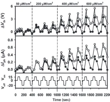
Fig. 3. ΔVTHLightand photocurrent difference ΔIphmeasured by applying a
periodic gate bias under various light intensities. The Vst
GSwaveform consists
of sequential four potential steps (15 V, 0,−20, and 0 V). ΔVTHLightand ΔIph
normalized to the initial value of every cycle is also shown by black circles.
at the dielectric/organic interface to bend down further. The number of electron-trapping states below the Fermi energy is increased. This allows more photogenerated electrons to be trapped and provides a larger response window to different
PL. Also, for a very weak light such as PL= 50 μW/cm2,
increasing Vst
GScan effectively enlarge ΔV Light
TH and Rph. If no stressed bias is applied on OPT, it is almost impossible to detect the weak light with PL= 50 μW/cm2. When VGSst = 30 V, the Rph of OPTs with L as 100 μm is 40 A/W under white-light irradiation (PL= 50 μW/cm2) and 92 A/W under
blue-LED irradiation (465 nm and 50 μW/cm2). It is summarized that increasing the gate bias during illumination can effectively increase the detection dynamic range and enhance the sensing ability related to very weak light intensity in the range of microwatts per square centimeter.
Finally, repeated sensing behavior is confirmed by applying a periodic gate bias onto devices during illumination. As shown in Fig. 3, the Vst
GSwaveform consists of four sequential potential steps (15, 0, −20, and 0 V). Every potential step has a 50-s duration. VGSst such as +15 V determines the sensing period.
Vst
GS such as−20 V is used to accelerate the recovery of the sensing signal. ΔVTHLightand photocurrent variations (ΔIph) are plotted as a function of time. ΔIphis defined as Iph–Iphini, where
Iini
ph is the drain current measured promptly under irradiation. Although long-time integration (several tens of seconds) is needed to obtain significant ΔIphand ΔVTHLight, its application on a large-area flexible scanner is possible. During scanning, OPTs are turned off (with a positive gate bias). They are turned on only in the signal reading cycles. This is beneficial for power savings. During the recovery period, an incomplete recovery is due to an incomplete compensation between electron and hole trapping and can be treated as noise. The noise can be eliminated if the variation of ΔVTHLightand ΔIphin the sensing period is used as a sensing index, as shown by the black symbols in Fig. 3.
IV. CONCLUSION
The ΔVTHLightand Rphof pentacene-based OPTs have been
greatly improved by applying a positive gate bias during il-lumination or by reducing the channel length. It is verified that even when the vertical electric field plays a dominant role in enhancing ΔVTHLight, the removal of light-induced holes through the source/drain electrodes is necessary to allow the light-induced electrons to be effectively trapped by the interface states. When increasing PL, the maximum ΔVTHLight of OPT was restricted owing to the fixed amount of interface trap states under a constant gate bias. Increasing the positive gate bias extends the response window to larger PLand improves Rphto very weak light. Finally, the repeated OPT response to different
PL is confirmed by applying a periodic voltage signal cycle.
These results are useful to design OPTs in image sensor array. To date, the origin of electron-trapping states is not clear. We had measured the devices in vacuum to suppress the influence of oxygen and water. A significant photoelectric field effect was still observed. Further studies need to be conducted to explore the mechanism in depth.
ACKNOWLEDGMENT
The authors thank Prof. H.-F. Meng for his helpful suggestion.
REFERENCES
[1] L. Zhou, A. Wanga, S.-C. Wu, J. Sun, S. Park, and T. N. Jackson, “All-organic active matrix flexible display,” Appl. Phys. Lett., vol. 88, no. 8, p. 083 502, Feb. 2006.
[2] H. S. Tan, T. Cahyadi, Z. B. Wang, A. Lohani, Z. Tsakadze, S. Zhang, F. R. Zhu, and S. G. Mhaisalkar, “Low-temperature-processed inorganic gate dielectrics for plastic-substrate-based organic field-effect transistors,”
IEEE Electron Device Lett., vol. 29, no. 7, pp. 698–700, Jul. 2008.
[3] M. Debucquoy, S. Verlaak, S. Steudel, K. Myny, J. Genoe, and P. Heremans, “Correlation between bias stress instability and phototran-sistor operation of pentacene thin-film tranphototran-sistors,” Appl. Phys. Lett., vol. 91, no. 10, p. 103 508, Sep. 2007.
[4] Y. Guo, C. Du, C.-A. Di, J. Zheng, X. Sun, Y. Wen, L. Zhang, W. Wu, G. Yu, and Y. Liu, “Field dependent and high light sensitive organic pho-totransistors based on linear asymmetric organic semiconductor,” Appl.
Phys. Lett., vol. 94, no. 14, p. 143 303, Apr. 2009.
[5] Y.-Y. Noh, D.-Y. Kim, and K. Yase, “Highly sensitive thin-film organic phototransistors: Effect of wavelength of light source on device perfor-mance,” J. Appl. Phys., vol. 98, no. 7, p. 074 505, Oct. 2005.
[6] K. Harada, M. Riede, K. Leo, O. R. Hild, and C. Michael Elliott, “Pentacene homojunctions: Electron and hole transport properties and related photovoltaic responses,” Phys. Rev. B, Condens. Matter, vol. 77, no. 19, p. 195 212, May 2008.
[7] M. C. Hamilton, S. Martin, and J. Kanicki, “Thin-film organic polymer phototransistors,” IEEE Trans. Electron Devices, vol. 51, no. 6, pp. 877– 885, Jun. 2004.
[8] R. A. Street, M. L. Chabinyc, F. Endicott, and B. Ong, “Extended time bias stress effects in polymer transistors,” J. Appl. Phys., vol. 100, no. 11, p. 114 518, Dec. 2006.
[9] R. R. Chance and C. L. Braun, “Intrinsic photoconduction in anthracene single crystals: Electric field dependence of hole and electron quantum yields,” J. Chem. Phys., vol. 59, no. 5, p. 2269, Sep. 1973.
[10] C. B. Park, T. Yokoyama, T. Nishimura, K. Kita, and A. Toriumi, “Molecular ordering and interface state modification for reducing bias-induced threshold voltage shift in pentacene field-effect transistors,”
J. Electrochem. Soc., vol. 155, no. 8, p. H575, 2008.
[11] H.-W. Zan and S.-C. Kao, “New organic phototransistor with bias-modulated photosensitivity and bias-enhanced memory effect,” IEEE