New Synthesis of Parallel-Coupled Line Bandpass
Filters With Chebyshev Responses
Kuo-Sheng Chin, Member, IEEE, Yi-Chyun Chiou, Student Member, IEEE, and Jen-Tsai Kuo, Senior Member, IEEE
Abstract—Parallel-coupled line filters with Chebyshev pass-bands are synthesized based on the insertion-loss functions derived by converting the composite matrices of all coupled stages. With the synthesis, both the electromagnetic simulation and measurement results have accurate in-band re-sponse and bandwidth. Simultaneous equations for Chebyshev filters of order 9 are derived for determining geometric parameters of the coupled stages. The tradeoff between circuit bandwidth and ripple level is discussed. In experiments, three planar or quasi-planar structures, including the coupled-line with aperture in the ground plane, the three-line microstrip, and the broadside-coupled lines, are employed to realize the end stages for implementing the high coupling levels. Experimental filters of order up to nine with fractional bandwidth of 30% or 40% are fabricated and measured. The results show good agreement with predictions by the theory and simulation.
Index Terms—Bandpass filters, Chebyshev response, insertion-loss function, parallel-coupled line filter, strong coupling.
I. INTRODUCTION
T
HE parallel-coupled configuration has been widely used for realization of microstrip bandpass filters [1]–[4]. Ap-proximate formulas have been well documented for determining dimensions of the coupled stages [3], [4]. These approximate formulas can provide accurate results when the filter order is low and the designated bandwidth is small. When the circuit order is higher or the bandwidth is increased, however, the bandwidth of the synthesized filter will be less than specification. For ex-ample, fifth-order filters have bandwidths of only 25% and 31% when designated bandwidths are 30% and 40%, respectively. The bandwidth decrement deteriorates as the designated band-width or filter order is increased [5]. The bandband-width decrement is due to the use of the equivalence of a coupled stage to two quarter-wave lines with a frequency-independent -inverter in between [3], [4]. It is noted that equivalence of a distributed net-work to a lumped element must have a limited bandwidth.Various methods have been proposed for synthesizing band-pass filters with accurate band-passband responses. For example, the
Manuscript received November 7, 2007; revised April 17, 2008. First pub-lished June 13, 2008; last pubpub-lished July 9, 2008 (projected). This work was supported in part by the Ministry of Education (MoE) under the ATU Plan and National Science Council, Taiwan, R.O.C., under Grant NSC 96-2221-E-182-002, Grant NSC 96-2752-E-009-003-PAE, and Grant NSC 95-2221-E-009-037-MY2.
K.-S. Chin is with the Department of Electronic Engineering, Chang Gung University, Taoyuan 333, Taiwan, R.O.C. (e-mail: [email protected]).
Y.-C. Chiou and J.-T. Kuo are with the Department of Communication Engi-neering, National Chiao Tung University, Hsinchu 300, Taiwan, R.O.C. (e-mail: [email protected]).
Color versions of one or more of the figures in this paper are available online at http://ieeexplore.ieee.org.
Digital Object Identifier 10.1109/TMTT.2008.925572
distribution method [6] provides solutions to quarter-wave-length-coupled structures and the insertion-loss function method activates the syntheses of short-circuited quarter-wave stub filters [7] and the parallel-coupled line filters [8]. Note that the circuits in [6]–[8] are limited to maximally flat responses.
Chebyshev filters are more flexible than the maximally flat type due to the degree of freedom for the tradeoff between the passband ripple level and rejection rate in the transition band. This paper extends our previous study on the maximally flat type in [8] to the synthesis of Chebyshev filters of higher or-ders. Simultaneous equations for solving the geometric param-eters of all coupled stages are derived based on the composite matrices, which take the full distributed property of each stage into account. It will be shown that the coupled stages, especially the end stages, require higher coupling levels than those of the conventional synthesis [3], [4]. In [8], tapped-line input/output is used to realize the high coupling since the gap size or linewidth of the end stages exceeds the resolution limit of the standard printed circuit board (PCB) technology. In this paper, the tapped-line structure is purposely bypassed and the end sections are realized by three substitutes for exploring their performances for implementing the high coupling levels. The first one is the coupled section with an aperture in the ground plane [9]. Enhanced coupling can be obtained by removing the conductor in the ground plane under the section. The second is the three-line microstrip [10]. When it is used to replace a usual coupled-line stage, for a given coupling level, some case studies show that the tight line spacing can be relaxed by six to seven times. The last one is the microstrip-to-coplanar wave-guide (CPW) broadside-coupled structure. This structure is well suitable for providing high coupling over a wide bandwidth. The ultra-wide bandwidth bandpass filter in [11] is a typical ex-ample. Based on this structure, some miniaturized ring devices [12], [13] have been developed.
This paper puts emphasis on the extension from [8] as fol-lows. First, for Chebyshev passbands, simultaneous equations for determining the modal characteristic impedances of each coupled stage are derived for circuits of order up to nine, in con-trast to the sixth-order Butterworth filters in [8]. The ripple level condition is then formulated and the tradeoff between the ripple level and bandwidth is discussed. Finally, the three structures with enhanced coupling are incorporated into the experiments, and measured responses are presented for validating the theory and electromagnetic (EM) simulation.
II. CHEBYSHEVPASSBANDS
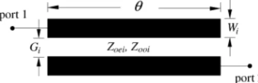
An th-order parallel-coupled line filter consists of a cas-cade of coupled stages is shown in Fig. 1. Herein, both the source and load impedances are assumed identical to the
Fig. 1. ith coupled stage with linewidth W and gap G .
system impedance . The matrix of the th stage can be expressed as [4], [8]
(1)
where is its electrical length, and
and and
are, respectively, the even- and odd-mode characteristic imped-ances of the coupled lines. The modal phase velocities of all coupled-lines are assumed identical.
It has been shown in [8] that the entries of the total
matrix of the filter are polynomials of and the coefficients are functions of and . The insertion loss function can be written as [3]
(2) where is power available from the source and is power delivered to the load. On the other hand, the insertion-loss func-tion of an th-order Chebyshev filter is defined as [3], [4]
(3) where defines the ripple level and is the Chebyshev polynomial of the first kind of order . The vari-ables and and, hence, the geometry parameters and , will be solved by matching (2) with (3).
A. Second-Order Filters
In this section, synthesis of a second-order Chebyshev filter is demonstrated. Due to structural symmetry, we have
and . It can be derived that
(4a) where
(4b)
(4c) (4d)
Substituting (4a) into (2), we have
(5a) where
(5b) and
(5c) In 5(c), is the total quality factor ( ) of the filter and is the electrical length of the coupled stage at the passband edge. It is important to note that a variable is purposely introduced to (5a). It provides one extra degree of freedom in matching the coefficients in (5a) with those in (3) and preserves the designated Chebyshev response at the same time.
Substituting into (3), we have
(6) Matching (5a) with (6) and enforcing
and , we have
(7a) (7b) (7c) Inserting (7) into (5a) yields
(8) The term will provide an equal-ripple response in the passband, and its coefficient not only defines the ripple level, but also implies a transmission zero at twice the design frequency, , where . Note that, in (7), there are five unknowns, i.e., and , to be determined. By imposing the given ripple level to (8), the system has four conditions and there is one degree of freedom for choosing the solution. If in (5a) the variable is not introduced, however, the system will be fully determined.
B. Filters of Order
When is increased, the derivation is straightforward. The insertion loss function, however, is long and tedious when is large. One can utilize the structural symmetry to reduce the number of variables and times of matrix multiplication. The si-multaneous conditions for solving and can be obtained by matching coefficients of the terms of the insertion
loss function with those of . Here, we derive the in-sertion-loss functions for filters of order , and the results are
(9)
(10) The simultaneous conditions are listed in Table I. It is found that holds for each , and it is also valid for the maximally flat filters [8]. Note that total number of unknowns ( and ) for such an th-order filter is , where is de-fined as the maximal integer no larger than . The number of conditions, including the specified ripple level, is less than that of unknowns when . In addition, the variable intro-duces an extra degree of freedom in matching the coefficients. It can be validated that the degrees of freedom for are . This under-determined feature is very useful for circuit realization.
III. RIPPLELEVEL ANDFRACTIONALBANDWIDTH
A. Ripple Level Specified by
In the conventional synthesis [3], [4], the edges of the pass-band of a Chebyshev pass-bandpass filter in (9) and (10) are defined by . If this idea is used, the so-called ripple-level condi-tion can be obtained by evaluating the funccondi-tions in (9) and (10) at in (5c). It leads to
(11)
(12) The in-band equal-ripple characteristic in (10) is expected to be provided by the Chebyshev function if its coefficient is a constant. The ripple levels within the passband, however, will be altered by the frequency-dependent term . Note that for an th-order Chebyshev bandpass filter, there are transmission poles and
peaks in the passband. Since the square of each is symmetric about , unequal in-band ripples will occur when . If a small bandwidth decrement is acceptable, part of the altered ripple can be recovered. To tackle this, a method for correcting the ripple is formulated as follows.
B. Ripple Level Specified by
The frequencies where peaks of ripples (in-band minima of or peaks of ) occur can be obtained by
(13)
Given the value, one can validate that the result is identical to that in (11) when . When , the ripple condition derived from (13) can be written as
(14a) where
(14b)
for . The ripple peaks will increase
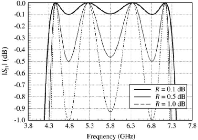
when moves away from the passband edge . For example, when , there are three ripple peaks with two levels in the passband. Fig. 2 shows the detailed responses of three fourth-order filters with % and
and dB. When and dB, the peak ripple levels at (center frequency) are 0.93 and 0.46 dB, respectively. When dB, the deviation seems negligible.
Obviously, application of (14) will lead to a decrement of bandwidth. The decrement depends on which is chosen. It is plausible to redefine the value at with as the ripple level of the filter since it has the maximal ripple within the passband and it results in the smallest bandwidth decrement. For example, when , there are four minima symmetri-cally locating on both sides of with two ripple levels. Based on the condition (14) with dB, when designated bandwidths are 40% and 50%, the calculated bandwidths are 39.7% and 49.6%, respectively. All these bandwidth decrements can be negligible. Our further studies show that the dependence of the decrements on the designated bandwidths and value (from 0.1 to 3 dB) is more or less the same for filters of orders . Thus, the condition will be used for the experimental demonstrations herein.
IV. SOLUTIONS ANDEXPERIMENTS
Based on the simultaneous equations in Table I, together with the ripple-level condition (12) or (14), the variables and of all coupled stages can be solved, and then the linewidth and
gap size can be determined by and
. The solution procedure can be referred to [8] and is briefly described as follows. For example, a fifth-order filter has two degrees of freedom for choosing the solution. One can take one of the six variables and as sweep variables to solve the equations. Since highly coupled structures have been planned to substitute the end stages, in the solution-searching procedure, one can relax the dimensions of the middle stages and locate all the difficulties to the end stages as much as possible. After all solutions with tough geometric parameters are removed, one obtains a solution range for each variable. The modal characteristic impedance design graph can be useful for the solution selection.
It is worth mentioning that change of will not alter the Chebyshev passband response, but will lead the coupled stages to have different modal characteristic impedances. Consider a
filter with % and dB. We can take
and as sweep variables to solve the simultaneous equations. Fig. 3 plots the root loci of and of the second and third
TABLE I
SIMULTANEOUSCONDITIONS FORSYNTHESIS OFCHEBYSHEVFILTERS OFORDERSN = 1–9
stages for and . The loci indicate that most of the solutions fall into the fan area of and .
As is increased, the values of and increase, while those of and decrease. In this particular
ex-Fig. 2. DetailedjS j responses in the passbands of fourth-order filters with 1 = 50% and R = 0:1; 0:5; and 1 dB.
Fig. 3. Root loci ofZ and Z of the second and third stages of fifth-order Chebyshev filters (1 = 40% and R = 0:1 dB) with k = 0:5; 1; and 2. Substrate:" = 10:2, thickness d = 1:27 mm.
ample, the case has the easiest circuit dimensions for realization.
Table II investigates the changes of the modal impedances of the coupled stages from the conventional synthesis to the pro-posed method for fifth-order filters with a 0.1-dB ripple and ranging from 10% to 50%. The listed solutions for the proposed method are selected since they are relatively easy to realize. In comparison of the listed data for %, one can see that middle stages of the proposed method have much narrower di-mensions than those of the conventional synthesis. In addition, the ratio of the end stages of the proposed method is much larger than that of the conventional synthesis. Note that, from Fig. 3, a larger ratio corresponds to a tighter gap size. The situation becomes even worse when the bandwidth is increased. For the conventional synthesis, the ratios are increased to around three only for the first stage when band-width is more than 40%. Table II also compares the bandband-width
TABLE II
MODALCHARACTERISTICIMPEDANCES OF THECOUPLEDSTAGES OFFIFTH-ORDERCHEBYSHEVFILTERS BY THEPROPOSED
METHOD ANDCONVENTIONALSYNTHESIS
decrements of the proposed method and the conventional syn-thesis. When % is given, the conventional synthesis
has %, while the proposed method has %.
When % is specified, the bandwidth of the conventional synthesis lacks of 12%, while the bandwidth decrement of the proposed method is only 2.5%.
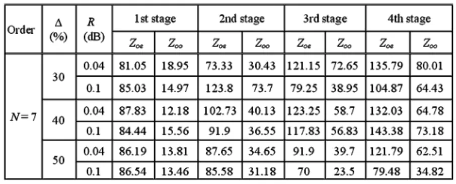
Table III lists the even- and odd-mode characteristic imped-ances of coupled stages of seventh-order Chebyshev filters with and dB and bandwidths from 30% to 50%. Again, these data are selected because of they are relatively easy to re-alize by the standard PCB process.
Herein, the RT/Duroid 6010 high-frequency laminate ( and thickness mm) is used as the circuit sub-strate. For demonstration, two filters ( and ) of order 5 with % and dB and one filter of order 9 with
% and dB, all designed at GHz,
are fabricated and measured. Ansoft’s software package High Frequency Structure Simulator (HFSS) [14] is used for EM sim-ulation.
1) Filters and % dB): When
, six variables have to be solved for the three leading stages. Given %, we have rad. The solution and is chosen for demonstration. The and values of each stage are listed in Table IV. The modal char-acteristic impedances of the end stages are and , and the corresponding linewidth and gap size for a usual coupled-line stage are 0.921 and 0.021 mm, respec-tively. Note that the gap size is much smaller than the best reso-lution of the standard microstrip technology. If the bandwidth is larger or the ripple is smaller, the gap size will be even tougher for fabrication.
An aperture in the ground plane can be created under the cou-pled lines to enhance the coupling [9]. It is due to the aperture, more field lines originating from one of the coupled lines ter-minate to the other so that the coupling can be enhanced. By treating a section of such coupled lines as a four-port, numer-ical data such as the -parameters can be obtained by Ansoft’s
TABLE III
MODALCHARACTERISTICIMPEDANCES()OFCOUPLEDSTAGES OFSEVENTH-ORDERCHEBYSHEVFILTERS
TABLE IV
SOLUTIONS ANDMODALCHARACTERISTICIMPEDANCES OF THESTAGES OF THETHREEEXPERIMENTALFILTERS
HFSS. The matrix pencil method [15] can then be used to ac-curately extract its phase constants and characteristic imped-ances. The electrical length of each stage is a quarter-wave long at frequency , which is the geometric mean of the even- and odd-mode phase velocities. To eliminate the open-end fringing effect, the EM simulator HFSS is employed to finely tune the length of each coupled stage. In (1), the modal phase velocities of all coupled lines are assumed identical. Its purpose is to sim-plify the derivation of the conditions listed in Table I. In prac-tice, it is well known that different modal phase velocities will cause spurious response at . We have proposed several approaches, e.g., [16] and [17], to tackle this problem. In the proposed synthesis, it is worth mentioning the assumption that equal modal phase velocities have a negligible effect on the ac-curacy of passband response and bandwidth.
Fig. 4 compares the measured and responses with the calculated results. The dashed curves are the theoretical data obtained by (10). In the experimental circuit, the aperture has a length identical to that of the coupled lines and a width of 7.45 mm. Its width is chosen wider than the distance between the outer edges of the coupled line to assure a sufficiently high coupling level. The measured data show good agreement with the simulation. Compared the theoretical prediction, the surement is short of only 0.9% bandwidth. The detailed mea-sured data show that the in-band is only 1.1 dB, which is acceptable for many applications. The ripple level of the curve is better than 14 dB, in contrast to the theoretical value 16.4 dB. The group delay in the passband is from 2 to 4 ns.
The end stages of the above fifth-order filter are also realized by three-line microstrip sections [10]. The three metal strips are equally spaced and have identical linewidths . By constructing a design graph like Fig. 3 , the geo-metric parameters of the sections can be determined. Fig. 5(a)
Fig. 4. Measured, simulated, and theoretical responses of filter . End cou-pled stages are realized by a coucou-pled-line section with a ground-plane aperture. Circuit dimensions:W = 2:75 mm, G = 0:15 mm, W = 0:97 mm, G = 0:16 mm, W = 0:15 mm, G = 0:724 mm. Substrate: " = 10:2; thickness = 1:27 mm.
plots the measured data together with the calculated responses. The practical and responses show even better agree-ment with the calculation than the previous demonstration. The in-band is also only 0.6 dB, and the peak is 16.6 dB. The measurement is, nevertheless, still short of 0.8% bandwidth. Fig. 5(b) shows a photograph of the experimental circuit.
The reason why the three-line circuit has better in-band performance and improved ripples could be due to the fact that it has no aperture on the ground plane, which may cause
Fig. 5. (a) Measured, simulated, and theoretical responses of filter . End coupled stages are realized by a three-line section. (b) Experimental circuit. W ; G ; W ; and G are identical to those in Fig. 4. Dimensions of the three-line stage:W = 0:475 mm, G = 0:13 mm.
power losses resulted from possible radiation. Note that the two substitutes for the end stages are required to implement iden-tical coupling levels. Since the gap size of the three-line struc-ture (0.13 mm) is smaller than that of the coupled lines with ground-plane aperture (0.15 mm), it is reasonable to deduce that the latter can offer higher coupling than the three-line structure when they have the same gap size. Of course, this deduction re-quires that the aperture width be large enough.
2) Filter % dB): The third
experiment uses the microstrip-to-CPW broadside-coupled sec-tions [11] to implement the end stages. Fig. 6 plots the structure of the broadside-coupled lines. To make the design simpler, the width of the microstrip is made identical to that of the active conductor of the CPW to reduce the number of geometric pa-rameters. The modal parameters of this asymmetric coupled line are extracted in a way similar to the two previous cases. Some transmission line characteristics of the broadside-coupled lines can be referred to [13].
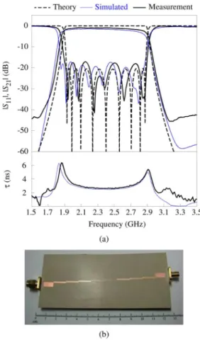
For a ninth-order filter, there are ten variables of five coupled sections to be solved. Given % and dB, the solution
and for is chosen for the experiment. This solution is chosen owing to that realization of all the middle sections is possible (minimal linewidth mm). Note that the end stages have to imitate a microstrip coupled stage with
and ; the linewidth
mm and gap size mm if a usual
coupled-Fig. 6. Microstrip-to-CPW broadside-coupled lines.
Fig. 7. (a) Theoretical, simulated, and measured responses of the ninth-order filter . (b) Fabricated circuit (top view). Dimensions: W = 4:4 mm, G = 1:38 mm, W = 0:52 mm, G = 0:22 mm, W = 0:37 mm, G = 0:40 mm, W = 0:38 mm, G = 0:35 mm, W = 0:13 mm, G = 0:47 mm.
line section is used. Fig. 7(a) plots the theoretical, simulated, and measured results. All of them show good agreement. The measured insertion loss is 0.99 dB, and the measured bandwidth is only 0.2% more than the theoretical response by (10). The maximal measured in-band return loss is 17.1 dB in contrast to the theoretical value of 20.3 dB. Fig. 7(b) is a photograph showing the top side of the experiment circuit.
Almost all microwave filters must be enclosed in a metal box in any practical application. For a given set of specifica-tions, only the geometric parameters of the coupled stages need changing since the and (or and ) values specify the passband. The apertures on the ground plane may cause ra-diation, which may affect the performances of the filter. The measured results of filters and indicate that the in-band are acceptable in most of practical applications. In the stopband, radiation could deteriorate the rejection level due to unwanted
coupling from portions of the filter directly to the output ter-minal. One possible way to solve the problem is to block the unwanted coupling path.
V. CONCLUSION
New and rigorous synthesis formulas have been derived for parallel-coupled line filters with Chebyshev responses for or-ders up to nine. The technique accurately predicts the passband response and circuit bandwidth. Simultaneous equations and the ripple-level conditions have been formulated and tabulated for determining the circuit dimensions. When filter order , the passband function has unequal ripple levels resulted from the term in the derived insertion-loss expressions. Three structures suitable for realizing high coupling levels have been incorporated into the end stages of the three experimental cir-cuits for validation of the formulation. All measured data show good performance and have good agreement with the theory and simulation.
ACKNOWLEDGMENT
The authors are grateful to the National Center for High Per-formance Computing, Hsinchu, Taiwan, R.O.C., for the HFSS software package and related services to this research.
REFERENCES
[1] S. B. Cohn, “Parallel-coupled transmission-line resonator filters,” IRE Trans. Microw. Theory Tech., vol. MTT-6, no. 4, pp. 223–231, Apr. 1958.
[2] C.-Y. Chang and T. Itoh, “A modified parallel-coupled filter structure that improves the upper stopband rejection and response symmetry,” IEEE Trans. Microw. Theory Tech., vol. 39, no. 2, pp. 310–314, Feb. 1991.
[3] G. L. Matthaei, L. Young, and E. M. T. Johns, Microwave Filters, Impedance Matching Networks, and Coupling Structures. Norwood, MA: Artech House, 1980.
[4] D. M. Pozar, Microwave Engineering, 2nd ed. New York: Wiley, 1998.
[5] K.-S. Chin, L.-Y. Lin, and J.-T. Kuo, “New formulas for synthesizing microstrip bandpass filters with relatively wide bandwidths,” IEEE Mi-crow. Wireless Compon. Lett., vol. 14, no. 5, pp. 231–233, May 2004. [6] J. M. Drozd and W. T. Joines, “Maximally flat quarter-wavelength-cou-pled transmission-line filters usingQ distribution,” IEEE Trans. Mi-crow. Theory Tech., vol. 45, no. 12, pp. 2100–2113, Dec. 1997. [7] W. W. Mumford, “Tables of stub admittances for maximally flat filters
using shorted quarter-wave stubs,” IEEE Trans. Microw. Theory Tech., vol. MTT-13, no. 9, pp. 695–696, Sep. 1965.
[8] K.-S. Chin and J.-T. Kuo, “Insertion loss function synthesis of maxi-mally flat parallel-coupled line bandpass filters,” IEEE Trans. Microw. Theory Tech., vol. 53, no. 10, pp. 3161–3168, Oct. 2005.
[9] M. D. C. Velázquez-Ahumada, J. Martel, and F. Medina, “Parallel coupled microstrip filters with ground-plane aperture for spurious band suppression and enhanced coupling,” IEEE Trans. Microw. Theory Tech., vol. 52, no. 3, pp. 1082–1086, Mar. 2004.
[10] J.-T. Kuo and E. Shih, “Wideband bandpass filter design with three line microstrip structures,” Proc. Inst. Elect. Eng., vol. 149, no. 5, pt. H, pp. 243–247, Oct. 2002.
[11] H. Wang, L. Zhu, and W. Menzel, “Ultra-wideband bandpass filter with hybrid microstrip/CPW structure,” IEEE Microw. Wireless Compon. Lett., vol. 15, no. 12, pp. 844–846, Dec. 2005.
[12] J.-T. Kuo, Y.-C. Chiou, and J.-S. Wu, “Miniaturized rat race coupler with microstrip-to-CPW broadside-coupled structure and stepped-impedance sections,” in IEEE MTT-S Int. Microw. Symp. Dig., Hon-olulu, HI, Jun. 2007, pp. 169–172.
[13] Y.-C. Chiou, J.-T. Kuo, and J.-S. Wu, “Miniaturized dual-mode ring resonator bandpass filter with microstrip-to-CPW broadside-coupled structure,” IEEE Microw. Wireless Compon. Lett., vol. 18, no. 2, pp. 97–99, Feb. 2008.
[14] High Frequency Structure Simulator (HFSS). ver. 9.2, Ansoft, Pitts-burgh, PA, 2004.
[15] Z. A. Mariievic, T. K. Sarkar, Y. Hua, and A. R. Djordjevic, “Time-domain measurements with the Hewlett-Packard network analyzer HP 8510 using the matrix pencil method,” IEEE Trans. Microw. Theory Tech., vol. 39, no. 3, pp. 538–547, Mar. 1991.
[16] J.-T. Kuo and M.-H. Wu, “Corrugated parallel-coupled line band-pass filters with multispurious suppression,” IET Microw. Antennas Propag., vol. 1, no. 3, pp. 718–722, Jun. 2007.
[17] J.-T. Kuo, U.-H. Lok, and M.-H. Wu, “Novel corrugated coupled-line stage with ideal frequency response and its application to bandpass filter design with multi-harmonic suppression,” in IEEE MTT-S Int. Mi-crow. Symp. Dig., Honolulu, HI, Jun. 2007, pp. 553–556.
Kuo-Sheng Chin (S’05–M’06) received the M.S.E.E. degree from Syracuse University, Syra-cuse, NY, in 1993, and the Ph.D. degree in com-munication engineering from National Chiao-Tung University, Hsinchu, Taiwan, R.O.C., in 2005.
In 1986, he joined the Chung Shan Institute of Science and Technology, Tao-Yuan, Taiwan, R.O.C., as Research Assistant, becoming an Assistant Scientist and then an Associate Scientist. He is currently an Assistant Professor with the Department of Electronic Engineering, Chang Gung University, Tao-Yuan, Taiwan, R.O.C. His main research interests are microwave measure-ments, microwave circuits, radome and antenna designs, and electromagnetic pulse (EMP) research.
Yi-Chyun Chiou (S’04) was born in Taoyuan,
Taiwan, R.O.C., on September 25, 1979. He re-ceived the B.S. and M.S. degrees in electronic engineering from Feng Chia University, Taichung, Taiwan, R.O.C., in 2001 and 2003, respectively, and is currently working toward the Ph.D. degree in communication engineering at National Chiao Tung University (NCTU), Hsinchu, Taiwan, R.O.C.
From 2003 to 2004, he was a Lecturer with the Department of Electronic Engineering, Nan Kai In-stitute of Technology, Nanto, Taiwan, R.O.C. His re-search interests include the design of microwave devices and RF modules for microwave and millimeter-wave applications.
Mr. Chiou was a corecipient of the 2007 Asia–Pacific Microwave Conference (APMC) Prize.
Jen-Tsai Kuo (S’88–M’92–SM’04) received the
Ph.D. degree from the Institute of Electronics, National Chiao Tung University (NCTU), Hsinchu, Taiwan, R.O.C., in 1992.
Since 1984, he has been with the Department of Communication Engineering, NCTU, where he is currently a Professor. From 1995 to 1996, he was a Visiting Scholar with the Electrical Engineering Department, University of California at Los Angeles (UCLA). Since February 2007, he has been the Secretary General of NCTU. His research interests include analysis and design of microwave integrated circuits and numerical techniques in electromagnetics.
Dr. Kuo is currently an Editorial Board member of the IEEE TRANSACTIONS ONMICROWAVETHEORY ANDTECHNIQUESand the IEEE MICROWAVE AND
WIRELESSCOMPONENTSLETTERS. He was a corecipient of the 2002 Best Paper Award presented at the National Telecommunication Conference, Taiwan, R.O.C., and a corecipient of the 2007 Asia–Pacific Microwave Conference (APMC) Prize. He was the recipient of the Taiwan Citation Laureate 2006 presented by Thomson Scientific and the 2007 Distinguished Research Award presented by the National Science Council, Taiwan, R.O.C.