IEEE TRANSACTIONS ON ELECTRON DEVICES, VOL. 57, NO. 12, DECEMBER 2010 3395
ESD Protection Design With Lateral DMOS
Transistor in 40-V BCD Technology
Chang-Tzu Wang, Student Member, IEEE, and Ming-Dou Ker, Fellow, IEEE
Abstract—An electrostatic discharge (ESD) protection design
for smart power applications with lateral double-diffused MOS (LDMOS) transistors is investigated. With the gate-driven and substrate-triggered circuit techniques, the n-channel LDMOS can be quickly turned on to protect the output drivers during an ESD stress event. The proposed gate-driven and substrate-triggered ESD protection circuits have been successfully verified in a 0.35-µm 5 V/40 V bipolar CMOS DMOS (BCD) process, which can sustain ESD voltages of 4 kV in human-body-model (HBM) and 275 V in machine-model (MM) ESD tests. In addition, the power-rail ESD protection design can also be achieved with a stacked structure to protect 40-V power pins without a latchup issue in the smart power integrated circuits.
Index Terms—Bipolar CMOS DMOS (BCD) process,
electrosta-tic discharge (ESD), ESD protection, latchup. I. INTRODUCTION
D
MOS power transistors have been commonly used as out-put drivers in smart power technologies [1], [2], including the automotive integrated circuits (ICs). Such high-voltage transistors are often self-protecting against an electrostatic dis-charge (ESD) stress. The DMOS devices were employed for the ESD protection of high-voltage pins by channel current under a gate biasing condition [3]. However, the high-voltage device with a large amount of finger numbers did not have a high ESD robustness after entering the snapback breakdown region. Such a device exhibits random and unconstrained failures during the snapback breakdown before reaching its intrinsic limitation [4]. The medium-sized drivers are usually not robust enough to pass the typical industrial ESD specifications of 2 kV for the human body model (HBM) [5] and 200 V for the machine model (MM) [6]. This is attributed to the current crowding effect among the multiple fingers and then inducing inhomogeneous triggering of the parasitic BJT to cause the nonuniform turn-on issue [7], [8]. Therefore, an additional ESD protection designManuscript received March 5, 2010; revised September 9, 2010; accepted September 9, 2010. Date of publication October 14, 2010; date of current version November 19, 2010. This work was supported in part by the National Science Council (NSC), Taiwan, under Contract NSC 98-2221-E-009-113-MY2, by the Ministry of Economic Affairs, Taiwan, under Grant 98-EC-17-A-01-S1-104, and by the United Microelectronics Corporation, Taiwan. The review of this paper was arranged by Editor M. Darwish.
C.-T. Wang is with the Nanoelectronics and Gigascale Systems Laboratory, Institute of Electronics, National Chiao Tung University (NCTU), Hsinchu 300, Taiwan, and also with the Electrostatic Discharge Engineering Department, Reliability Technology and Assurance Division, United Microelectronics Cor-poration, Hsinchu 300, Taiwan.
M.-D. Ker is with the Nanoelectronics and Gigascale Systems Laboratory, Institute of Electronics, NCTU, Hsinchu 300, Taiwan, and also with the De-partment of Electronic Engineering, I-Shou University, Kaohsiung 840, Taiwan (e-mail: [email protected]).
Digital Object Identifier 10.1109/TED.2010.2079530
is needed to protect such output drivers in the high-voltage technologies [9].
To improve the turn-on speed of MOS transistors for the ESD protection, a resistance_capacitance-based ESD protection de-sign (with a MOS capacitor) has been widely used in advanced CMOS processes [10]. However, no MOS capacitor is available to sustain the high-voltage operation due to the thin gate oxide structure of the lateral DMOS transistor (e.g., Vd= 40 V and Vg= 5 V) in such a high-voltage technology studied in this work. If the MOS capacitor is implemented by such thin gate oxide and biased at a high voltage level, the overstress voltage will damage the thin gate oxide. Furthermore, the ESD ballast resistor of several hundred ohms is forbidden to be placed between the output pad (O/P) and the output driver, which was often designed with a specification of small turn-on resistance in applications. In such a case, the additional ESD protection circuit is placed in parallel with the output driver from the pad to the ground. If the additional ESD protection circuit was not turned on quickly enough, the output driver would be damaged during an ESD stress event. Therefore, it is important to develop an efficient ESD protection circuit that can effectively protect the high-voltage output drivers for various applications.
In this paper, two efficient ESD protection designs with n-channel lateral DMOS (LDNMOS) transistors are proposed without suffering the gate oxide reliability under the normal cir-cuit operation. With the gate-driven and the substrate-triggered circuit techniques, the turn-on speed of the LDNMOS device can be improved during an ESD stress event. Such an ESD protection design with the gate-driven ESD detection circuit can be further modified to achieve a latchup-free power-rail ESD protection circuit for the high-voltage power pins. The proposed ESD protection circuits have been successfully verified in a 0.35-µm 5 V/40 V bipolar CMOS DMOS (BCD) process.
II. CHARACTERISTICS OFLDNMOS WITHGATE-BIASED ANDSUBSTRATE-TRIGGEREDEFFECTS
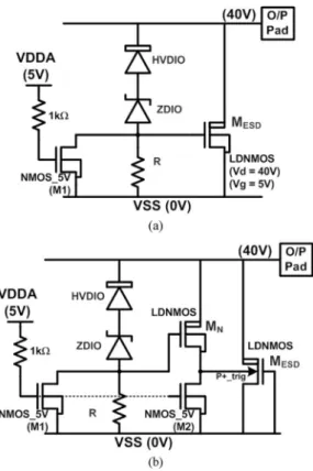
The device cross-sectional view and the layout top view of the LDNMOS with a field oxide (FOX) located at the drain region in a 0.35-µm 5 V/40 V BCD process are shown in Fig. 1(a) and (b), respectively. The gate oxide thickness of such a device is only 14 nm, limiting the maximum applicable gate voltage to 5 V. The N-drift and the P-body layers in Fig. 1(a) are lightly doped regions. The device is completely surrounded by the deep n-well (DNW) structure. The LDNMOS used as the ESD clamp device in the ESD protection circuit is drawn in multiple octagonal cells, as shown in Fig. 1(b). The side length of the octagon is 10 µm (the channel length of each
3396 IEEE TRANSACTIONS ON ELECTRON DEVICES, VOL. 57, NO. 12, DECEMBER 2010
Fig. 1. (a) Device cross-sectional view and (b) layout top view of the octagonal unit cell of the LDNMOS with 5-V gate oxide and 40-V drain-to-source operating voltage in a 0.35-µm 5 V/40 V BCD process.
Fig. 2. After a 3-kV HBM ESD stress, the failure spots were found only at a few contacts at the drain side of the LDNMOS drawn with the multiple-finger structure.
side), and therefore, the perimeter of each cell is 80µm. The P+_trig regions at the four corners are drawn as the trigger nodes for implementation of the substrate-triggered technique. In the traditional multiple-finger structure, the P-body regions of all fingers are fully separated by the FOX, and the individual P-body regions could worsen the nonuniform turn-on behavior of the LDNMOS device. Fig. 2 shows the ESD failure location of the gate-grounded LDNMOS device drawn by a traditional multiple-finger structure after a 3-kV HBM ESD stress. Only a few contacts were damaged at the drain diffusion during an ESD stress event. Therefore, the nonuniform turn-on phenom-enon among the multiple fingers of the LDNMOS device is easily observed, and the ESD robustness is hard to be improved
by only increasing the device dimension. On the other hand, the P-body regions at the source side are connected to each other if the LDNMOS is constructed by multiple octagonal cells with the P+_trig regions located around the LDNMOS. The LDNMOS can be assembled by multiple cells of row num-ber and column numnum-ber to reach a larger total device width for higher current conducting capability. In this paper, the LDNMOS is built up by 2× 2 octagonal cells, and the equiva-lent total device width is 320µm, as shown in Fig. 3. Moreover, such an octagonal structure can be applied for the gate-biased technique or the substrate-triggered technique (which is widely used in CMOS process [11]) by connecting the gate node or the P+_trig node to the bias/trigger circuits. To clarify the effec-tiveness of the gate-biased and substrate-triggered techniques on a high-voltage (HV) LDNMOS device, the technology computer-aided design (TCAD) simulation study is performed in the following. The device structure of the LDNMOS for TCAD simulation for this work is shown in Fig. 4.
A. LDNMOS With the Gate-Biased Technique
The TCAD-simulated I–V curves of the LDNMOS with different gate-biased conditions are shown in Fig. 5. Without the bias voltage on the gate terminal(Vg = 0 V), the trigger voltage of the LDNMOS is around 58 V. When the bias voltage is increased, the channel current is generated to improve the turn-on speed of the parasitic n-p-n bipolar junction transistor (NPN BJT) (DNW/P_Body/N+), and then, the trigger voltage of the LDNMOS can be reduced. The trigger voltage can be reduced to 47 V when a 5-V bias is applied at the gate of the
WANG AND KER: ESD PROTECTION WITH DMOS TRANSISTOR IN 40-V BCD TECHNOLOGY 3397
Fig. 3. Layout top view of an LDNMOS, which is constructed by 2 × 2 octagonal cells. In this structure, the P_Body regions of all the cells are connected to each other.
Fig. 4. Device structure of the LDNMOS for TCAD simulation.
Fig. 5. TCAD-simulatedI–V curves (IDS_VDS) of the LDNMOS device with different gate biases.
LDNMOS. To compare the difference between the LDNMOS device with and without gate bias, the I–V curves of the LDNMOS with Vgs of 0 and 5 V are replotted in full scale and shown in Fig. 6(a). Points a, b, c, and d are marked on the curves to compare the corresponding electric field distribution under VDSs of 10 and 47 V (the trigger voltage of LDNMOS with Vg of 5 V). The electric field distribution of the LDNMOS with Vg of 0 V at points a and b of theI–V curve are shown in Fig. 6(b). Without gate bias voltage, the electric field
distri-Fig. 6. (a) TCAD-simulatedI–V curves of the LDNMOS device and the corresponding electric field distribution of the LDNMOS device with Vg of (b) 0 V and (c) V under VDS of 10 V and VDS of 47 V.
bution localizes at the FOX edge, and no turn-on phenomenon appears even if the VDS is increased to 47 V. On the other hand, the electric field distribution of the LDNMOS with Vg of 5 V at the points c and d of theI–V curve are shown in Fig. 6(c). With a gate bias of 5 V, the channel current along the surface can release the amplitude of the electric field and accelerate the turned-on speed of the parasitic NPN BJT in LDNMOS. When the VDS is increased to 47 V, the LDNMOS is going to enter the snapback region, and the localization of electric field
3398 IEEE TRANSACTIONS ON ELECTRON DEVICES, VOL. 57, NO. 12, DECEMBER 2010
Fig. 7. (a) TCAD-simulatedI–V curves of the LDNMOS device with differ-ent substrate-triggered currdiffer-ents (I_trig) and (b) the electric field distribution at VDS of 10 V and VDS of 45 V under I_trig of 1 mA/µm.
distribution is shifting from the FOX edge to the N_Drift region at the drain side. From the simulation, the gate-biased technique can improve the turn-on behavior of the LDNMOS device.
B. LDNMOS With the Substrate-Triggered Technique
The TCAD-simulated I–V curves of the LDNMOS with different substrate-triggered currents (I_trig) are shown in Fig. 7(a). The substrate-triggered current flowing from P_trig to N+ region at the source side will provide the base current of the parasitic NPN BJT to trigger it on. When the substrate-triggered current is higher than 0.5 mA/µm, the trigger voltage of the LDNMOS will be reduced. With I_trig of 1 mA/µm, the trigger voltage is reduced to 45 V. The electric field distributions of the LDNMOS with I_trig of 1 mA/µm at point e (under VDS of 10 V) and point f (under VDS of 45 V) of theI–V curve are shown in Fig. 7(b). In the simulation, the substrate-triggered current flowing from the P_trig to N+ region is obvious, and it generates a voltage difference between the base and the emitter of the parasitic NPN BJT to trigger on the LDNMOS. Therefore, the substrate-triggered technique is also a useful method for accelerating the turn-on speed of the LDNMOS device for ESD protection.
Fig. 8. TCAD-simulated transient behaviors of the LDNMOS with and without (a) gate-biased voltage or (b) substrate-triggered current, where a 5-mA/µm current pulse with a rise time of 10 ns is applied to the drain side of the LDNMOS.
C. Transient Behavior of LDNMOS With Gate-Biased and Substrate-Triggered Techniques
The transient behaviors of the LDNMOS and the LDNMOS with the gate-biased and the substrate-triggered techniques under fast-transient ESD-like event are shown in Fig. 8(a) and (b), where a 5-mA/µm current pulse with a rise time of 10 ns is applied to the drain side of the LDNMOS in this simulation. In Fig. 8(a), the LDNMOS with Vg of 0 V is turned on when the drain voltage is higher than 57 V. However, the LDNMOS with Vg of 5 V can be accelerated to be turned on when the drain voltage is higher than 45 V. On the other hand, the LDNMOS with I_trig of 1 mA/µm can be turned on when the drain volt-age is higher than 35 V, as shown in Fig. 8(b). From the TCAD simulation, the turn-on period of LDNMOS can be shortened by applying the gate-biased or the substrate-triggered effects.
III. IMPLEMENTATION OFESD PROTECTION
CIRCUITWITHLDNMOS
The proposed ESD protection designs with the gate-driven ESD detection circuit (gate-biased technique) and the substrate-triggered ESD detection circuit are shown in Fig. 9(a) and (b),
WANG AND KER: ESD PROTECTION WITH DMOS TRANSISTOR IN 40-V BCD TECHNOLOGY 3399
Fig. 9. Proposed ESD protection circuits with (a) gate-driven and (b) substrate-triggered ESD detection circuits.
respectively, which are named as the gate-driven ESD protec-tion circuit and the substrate-triggered ESD protecprotec-tion circuit in this paper. The ESD clamp device(MESD) is implemented by the LDNMOS with 2× 2 octagonal cells, as discussed in Section II. In Fig. 9(a), the gate-driven ESD detection circuit is composed of a 40-V HV diode (HVDIO), a 7-V Zener diode (ZDIO), a 10-kΩ resistor (R), and a 5-V NMOS device (M1). The reverse-biased HVDIO and the ZDIO are connected in series to sustain the high-voltage (40 V) applications on the O/P during the normal circuit operating condition. A margin of 7 V from the total breakdown voltage of the diodes to the operating voltage is used to avoid mistriggering on the LDNMOS, even if a 10% overshooting voltage happens to the pad. Therefore, the gate-driven ESD protection circuit can be ensured against the gate oxide overstress issue under the normal circuit operating condition. The gate of M1 is connected to the low-voltage power supply (VDDA). The turned-on NMOS (M1) keeps the gate of the LDNMOS at VSS, so the ESD clamp device(MESD) is guaranteed to be kept off during the normal operating condition. When a positive fast-transient ESD voltage is applied to the O/P with VSS grounded and VDDA floating, the HVDIO and the ZDIO will enter the breakdown mode to conduct some of ESD current across the resistor R to generate a bias voltage to the gate ofMESD. Therefore, the gate voltage ofMESDcan be quickly pulled up to turn itself on by the gate-biased technique during ESD stress. After that, the ESD clamp device enters the snapback region to discharge the ESD current from the O/P to VSS. The VDDA is initially floating with an initial voltage level of∼0 V during an ESD stress event, so M1 is kept in theOFF-state without an influence on the operation of
the ESD clamp device.
In Fig. 9(b), the substrate-triggered ESD protection circuit in-cludes not only the HVDIO, ZDIO, R, and M1 (which are used in gate-driven ESD detection circuit), but also an additional LDNMOS(MN) as driving element and a 5-V NMOS device (M2). The gates of M1 and M2 are connected to VDDA to keep the voltage levels at the gate ofMN and the P+_trig node of the ESD clamp device(MESD) at VSS. During the ESD transient event, the driving elementMN is turned on by the gate-biased effect from the diodes in breakdown mode and then generates some channel current through MN into the P+_trig node of
the ESD clamp device(MESD). The substrate-triggered effect can be accomplished to accelerate the turn-on speed of the ESD clamp device.
IV. EXPERIMENTALRESULTS
The proposed ESD protection circuits have been fabricated in a 0.35-µm 5 V/40 V BCD process. No any additional mask layer is needed to fabricate the proposed ESD protection circuits. The typical gate-coupled LDNMOS, by connecting a resistor from its gate to VSS, has been also fabricated in the same wafer for comparison with the proposed gate-driven and the substrate-triggered ESD protection circuits. The gate-coupled LDNMOS is drawn by a multiple-finger structure with each finger width of 75 µm, and the total device width is 300 µm. On the other hand, the ESD clamp device in the proposed ESD protection circuits are drawn by 2× 2 octagonal cells with an equivalent total device width of 320µm. To inves-tigate the device behavior during ESD stress, the transmission line pulsing (TLP) technique [12] has been widely used to measure the trigger voltage (Vt1) and the secondary breakdown current (It2) of the ESD devices. The TLP generator with a pulsewidth of 100 ns and a rise time of 10 ns is used in this work to find the Vt1 and It2 of the LDNMOS with the gate-biased or substrate-triggered technique. The HBM ESD levels and the MM ESD levels of the ESD protection circuits are measured by the KeyTek ZapMaster, and the failure criterion is defined as theI–V characteristic curve shifting over 20% from its orig-inal curve after three continuous ESD zaps at every ESD test level.
A. TLP Characteristics of Stand-Alone LDNMOS With Gate-Biased or Substrate-Triggered Effects
The TLP-measured I–V characteristics of the LDNMOS device drawn by 2× 2 octagonal cells with an equivalent total device width of 320 µm under different gate-biased voltages (Vg) are shown in Fig. 10. Without any gate-biased voltage, the Vt1 of the LDNMOS device is ∼60 V. When the gate-biased voltage is increased to 1, 3, and 5 V, the Vt1 of the LDNMOS device is reduced to around 57, 50.5, and 48 V, respectively. With gate-biased voltages of 8 and 10 V, the Vt1 of the LDNMOS device can be reduced to ∼40 V. The TLP-measured I–V characteristics of the LDNMOS device drawn by 2× 2 octagonal cells with an equivalent total device width of 320µm under different substrate-triggered currents (I_trig) are shown in Fig. 11. When the applied substrate-triggered current is higher than 130 mA (equivalent to 0.4 mA/µm), the parasitic
3400 IEEE TRANSACTIONS ON ELECTRON DEVICES, VOL. 57, NO. 12, DECEMBER 2010
Fig. 10. TLP-measuredI–V curves of the LDNMOS device drawn by 2 × 2 octagonal cells with a device width of 320µm under different gate-biased voltages (Vg).
Fig. 11. TLP-measuredI–V curves of the LDNMOS device by with 2 × 2 octagonal cells with a device width of 320µm under different substrate-triggered currents (I_trig).
NPN BJT in the LDNMOS device starts to be turned on, and the Vt1 of the LDNMOS device is reduced. When the I_trig is increased to 0.5 and 0.55 mA/µm, the Vt1 can be reduced to 45 and 23 V, respectively. When the I_trig is higher than 0.6 mA/µm, the LDNMOS can be turned on rapidly to enter the snapback region without the breakdown mechanism, so the Vt1 is observed as∼11 V. From the experimental results of the TLP characteristics of the LDNMOS device with a gate-biased voltage and a substrate-triggered current, the acceleration to the turn-on speed of LDNMOS device can be achieved by the gate-biased or the substrate-triggered techniques.
To further evaluate the turn-on behaviors of the LDNMOS with gate-biased effects, the measured voltage waveforms clamped by the LDNMOS under different TLP voltage levels are shown in Fig. 12(a)–(f), where the rise time and the width of the applied pulse is 10 and 100 ns, respectively. In Fig. 12, with a higher gate-biased voltage, the LDNMOS can be turned on under a smaller applied TLP voltage. The applied 54-V TLP voltage can be clamped by the LDNMOS with Vg of 5 V. However, at that time, the LDNMOS without any gate-biased voltage is still inactive. When the applied TLP voltage is as high as 60 V, the LDNMOS with all the gate-biased conditions
can be turned on, but the turn-on time to clamp the applied voltage is different for each condition. The turn-on time to clamp the applied voltage can be shortened when the gate-biased voltage is increased. On the other hand, the measured voltage waveforms clamped by the LDNMOS with different substrate-triggered currents under different TLP voltage levels are shown in Fig. 13(a)–(d). Under a TLP applied voltage of 50 V, the LDNMOS with I_trig higher than 0.5 mA/µm can be turned on when the voltage is higher than 30 V. From these results, the acceleration of the turn-on speed by the gate-biased or the substrate-triggered effects can be verified.
B. ESD Performance of LDNMOS With Gate-Coupled Design
The TLP-measuredI–V characteristics of the gate-coupled LDNMOS with resistances of 10 and 50 kΩ are shown in Fig. 14. The trigger voltage of the gate-coupled LDNMOS with device width of 300µm is still ∼60 V, which is the same as the Vt1 of the standalone gate-grounded LDNMOS with the same device width. Moreover, there is no obvious difference between these two conditions with resistances of 10 and 50 kΩ because the parasitic capacitance from gate to drain of the LDNMOS device is too small to couple sufficient transient voltage to the gate for triggering on the LDNMOS device.
C. ESD Performance of LDNMOS With Gate-Driven and Substrate-Triggered ESD Detection Circuits
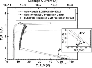
The TLP-measured I–V characteristics of the gate-driven ESD protection circuit and the substrate-triggered ESD protec-tion circuit are shown in Fig. 15, where theI–V characteristic of the gate-coupled LDNMOS with a resistance of 10 kΩ is also plotted into the figure for comparison. As seen in Fig. 15, the LDNMOS starts to be turned on by the gate-driven or the substrate-triggered ESD detection circuit when the applied voltage is higher than 47 V. The Vt1 of the LDNMOS with the gate-driven ESD detection circuit and the substrate-triggered ESD detection circuit can be reduced to ∼55 and ∼51 V, respectively. From the TLP-measured I–V curves, both the gate-driven and the substrate-triggered ESD detection circuits are effective in triggering the LDNMOS device, where the substrate-triggered ESD detection circuit gains more benefits to reduce the Vt1. However, it needs an additional device
MN as the driving element, which will occupy some
lay-out area. The leakage current of the gate-coupled LDNMOS was obviously increased when the TLP current is higher than 2.1 A. The failure criterion for the It2 measurement is de-termined by leakage current increasing by 30% compared to that of fresh samples in this work. Therefore, the It2 level of the gate-coupled LDNMOS is determined as 2.1 A. However, the It2 of the LDNMOS drawn by 2× 2 octagonal cells with the gate-driven and the substrate-triggered ESD detection circuits can be improved up to 2.6 and 2.7 A, respectively.
The HBM and MM ESD levels of the gate-coupled LDNMOS, the gate-driven ESD protection circuit, and the substrate-triggered ESD protection circuit are listed in Table I. The gate-coupled LDNMOS has ESD levels of 3 kV in HBM and 200 V in MM ESD tests. With the gate-driven ESD
WANG AND KER: ESD PROTECTION WITH DMOS TRANSISTOR IN 40-V BCD TECHNOLOGY 3401
Fig. 12. Measured voltage waveforms clamped to verify the turn-on efficiency of the LDNMOS with different gate-biased voltage by applying a TLP voltage pulse with the voltage level of (a) 46 V, (b) 50 V, (c) 54 V, (d) 56 V, (e) 58 V, and (f) 60 V.
detection circuit, the HBM and the MM ESD levels of the LDNMOS can be improved to 4.4 kV and 275 V, respectively. With the substrate-triggered ESD protection circuit, the HBM and the MM ESD levels of the LDNMOS are 4.2 kV and 275 V, respectively. No obvious difference in the ESD robust-ness of the LDNMOS device with these two ESD detection circuits because each octagonal cell of the LDNMOS device can be turned on uniformly. If a higher ESD level is desired,
the number of the octagonal cells in the LDNMOS should be increased to sustain the ESD stress.
D. Failure Analysis
The experimental results have shown that the trigger voltage of the LDNMOS device can be substantially reduced by the gate-driven and the substrate-triggered ESD detection circuits.
3402 IEEE TRANSACTIONS ON ELECTRON DEVICES, VOL. 57, NO. 12, DECEMBER 2010
Fig. 13. Measured voltage waveforms clamped to verify the turn-on efficiency of the LDNMOS with different substrate-triggered current by applying a TLP voltage pulse with the voltage level of (a) 50 V, (b) 52 V, (c) 56 V, and (d) 60 V.
Fig. 14. TLP-measuredI–V characteristics of the gate-coupled LDNMOS (drawn by multiple-finger structure with a width of 300µm) with resistances of 10 and 50 kΩ connected from gate to source.
Failure analyses carried by the scanning electron microscope [13] images provide the visual evidence to the LDNMOS device drawn in multiple octagonal cells, which can be triggered on
Fig. 15. TLP-measuredI–V characteristics of the LDNMOS with the pro-posed ESD detection circuits and the gate-coupled LDNMOS.
uniformly by the ESD detection circuit. Fig. 16 shows the ESD failure locations on the proposed gate-driven ESD protection circuit after a 4.6-kV positive-to-VSS HBM ESD stress. The failure spots were found at the drain contacts in each cell of
WANG AND KER: ESD PROTECTION WITH DMOS TRANSISTOR IN 40-V BCD TECHNOLOGY 3403
TABLE I
COMPARISON OFESD ROBUSTNESSAMONG THEGATE-COUPLED
LDNMOS, GATE-DRIVENESD PROTECTIONCIRCUIT,AND
SUBSTRATE-TRIGGEREDESD PROTECTIONCIRCUIT
Fig. 16. After a 4.6-kV HBM ESD stress, the failure spots were found at the drain contacts of each unit cell of the LDNMOS device with the gate-driven ESD protection circuit.
the LDNMOS device, indicating that the LDNMOS device has been uniformly turned on by the proposed gate-driven ESD detection circuit.
V. POWER-RAILESD PROTECTIONDESIGN
From the TLP-measuredI–V characteristic in Fig. 15, the snapback holding voltage of LDNMOS with the gate-driven or substrate-triggered ESD detection circuit is ∼12 V, which is smaller than the HV power supply voltage (VDD_HV) of 40 V. Such an ESD element used in the power-rail ESD protection circuit may be mistriggered on by the system-level ESD tran-sient pulse to cause a latchup failure [14], [15]. To overcome the latchup issue between the power rails, the stacked-LDNMOS structure is used to increase the total holding voltage. With the gate-driven ESD detection circuit, the trigger voltage of the stacked-LDNMOS structure can still be kept the same as that of the design in Fig. 9(a). The circuit diagram of the stacked-LDNMOS structure (four stacked-LDNMOS devices in series, where each LDNMOS is drawn by multiple-finger structure with a width of 300µm) with the gate-driven ESD detection circuit is shown in Fig. 17(a). The corresponding TLP-measuredI–V characteristic is shown in Fig. 17(b). During an ESD stress, the stacked-LDNMOS can be triggered into the snapback region to discharge the ESD current. With a total holding voltage of
Fig. 17. (a) Latchup-free ESD protection circuit realized with four stacked-LDNMOS devices and the gate-driven ESD detection circuit for 40-V power pins and (b) the corresponding TLP-measuredI–V characteristics.
∼50 V, the latchup issue can be successfully overcome for
40-V applications [16]. Therefore, the latchup-free power-rail ESD protection circuit can be safely applied in IC products with a high-voltage power supply voltage of 40 V. The It2 level is still kept at ∼2.5 A, so the ESD performance of the stacked-LDNMOS structure with the gate-driven ESD detection circuit can be kept as good as that of a single LDNMOS device. Of course, the stacked-LDNMOS can also be implemented with the layout of octagonal cells in the power-rail ESD protection circuit.
VI. CONCLUSION
The device characteristics of the LDNMOS with the gate-biased and the substrate-triggered effects have been inves-tigated in details by the TCAD simulation and the TLP measurement. Based on such device behaviors, two ESD protection circuits cooperated with LDNMOS transistors for 40-V O/P have been successfully verified in a 0.35-µm 5 V/ 40 V BCD process. The proposed ESD protection circuits with the gate-driven and the substrate-triggered techniques have performed the efficient turn-on uniformity with robust
3404 IEEE TRANSACTIONS ON ELECTRON DEVICES, VOL. 57, NO. 12, DECEMBER 2010
ESD levels, which are excellent design solutions to protect the high-voltage output drivers for smart power applications. By using the stacked-LDNMOS structure with the gate-driven ESD detection circuit, the latchup-free ESD protection circuit can be achieved for protecting the high-voltage power pins.
ACKNOWLEDGMENT
The authors would like to thank the United Microelectronics Corporation, Hsinchu, Taiwan, for the chip fabrication and T.-H. Tang for his valuable technical discussion.
REFERENCES
[1] B. Murari, F. Bertoti, and G. A. Vignola, Smart Power ICs: Technologies
and Applications. Berlin, Germany: Springer-Verlag, 2002.
[2] P. Wessels, M. Swanenberg, H. Zwol, B. Krabbenborg, H. Boezen, M. Berkhout, and A. Grakist, “Advanced BCD technology for automo-tive, audio and power applications,” Solid State Electron., vol. 51, no. 2, pp. 195–211, Feb. 2007.
[3] C. Duvvury, F. Carvajal, C. Jones, and D. Briggs, “Lateral DMOS design for ESD robustness,” in IEDM Tech. Dig., 1997, pp. 375–378.
[4] Y. Chung, H. Xu, R. Ida, W.-G. Min, and B. Baird, “ESD scalability of LDMOS devices for self-protected output drivers,” in Proc. IEEE. Int.
Symp. Power Semicond. Devices ICs, 2005, pp. 351–354.
[5] Standard Test Method for Electrostatic Discharge Sensitivity Testing—
Human Body Model (HBM)—Component Level, ESD STM5.1-2001,
2001.
[6] Standard Test Method for Electrostatic Discharge Sensitivity Testing—
Machine Model (MM)—Component Level, ESD STM5.2-199, 1999.
[7] M. P. J. Mergens, W. Wilkening, S. Mettler, H. Wolf, A. Stricker, and W. Fichtner, “Analysis of lateral DMOS power devices under ESD stress conditions,” IEEE Trans. Electron Devices, vol. 47, no. 11, pp. 2128– 2137, Nov. 2000.
[8] R. M. Steinhoff, J.-B. Huang, P. L. Hower, and J. S. Brodsky, “Current filament movement and silicon melting in an ESD-robust DENMOS tran-sistor,” in Proc. EOS/ESD Symp., 2003, pp. 98–107.
[9] B. Keppens, M. P. J. Mergens, C. S. Trinh, C. C. Russ, B. V. Camp, and K. G. Verhaege, “ESD protection solutions for high voltage technologies,” in Proc. EOS/ESD Symp., 2004, pp. 289–298.
[10] M.-D. Ker, “Whole-chip ESD protection design with efficient VDD-to-VSS ESD clamp circuit for submicron CMOS VLSI,” IEEE Trans.
Elec-tron Devices, vol. 46, no. 1, pp. 173–183, Jan. 1999.
[11] T.-Y. Chen and M.-D. Ker, “Investigation of the gate-driven effect and substrate-triggered effect on ESD robustness of CMOS devices,” IEEE
Trans. Device Mater. Rel., vol. 1, no. 4, pp. 190–203, Dec. 2001.
[12] T. J. Maloney and N. Khurana, “Transmission line pulsing techniques for circuit modeling of ESD phenomena,” in Proc. EOS/ESD Symp., 1985, pp. 49–54.
[13] J. Goldstein, D. E. Newbury, P. Echlin, C. E. Lyman, D. C. Joy, E. Lifshin, L. Sawyer, and J. R. Michael, Scanning Electron Microscopy and X-Ray
Microanalysis, 3rd ed. New York: Springer-Verlag, 2003.
[14] R. Lewis and J. Minor, “Simulation of a system level transient-induced latchup event,” in Proc. EOS/ESD Symp., 1994, pp. 193–199.
[15] M.-D. Ker and S.-F. Hsu, “Physical mechanism and device simulation on transient-induced latchup in CMOS ICs under system-level ESD test,”
IEEE Trans. Electron Devices, vol. 52, no. 8, pp. 1821–1831, Aug. 2005.
[16] M.-D. Ker and S.-F. Hsu, Transient-Induced Latchup in CMOS Integrated
Circuits. Hoboken, NJ: Wiley, 2009.
Chang-Tzu Wang (S’06) received the B.S. and
Ph.D. degrees from the National Chiao Tung University, Hsinchu, Taiwan, in 2005 and 2010, respectively.
In 2006, he joined the Electrostatic Discharge Engineering Department, Reliability Technology and Assurance Division, United Microelectronics Corpo-ration, Hsinchu, where he is currently an Assistant Manager and in charge of supervising the electro-static discharge (ESD) development for advanced CMOS processes. He is also with the Nanoelectron-ics and Gigascale Systems Laboratory, Institute of ElectronNanoelectron-ics, National Chiao Tung University (NCTU), Hsinchu. His technical area of expertise includes on-chip ESD protection circuit design for advanced CMOS processes, mixed-voltage I/O circuits, and high-speed/low-power applications.
Ming-Dou Ker (S’92–M’94–SM’97–F’08) received
the Ph.D. degree from the National Chiao Tung University (NCTU), Hsinchu, Taiwan, in 1993.
He was a Department Manager with the VLSI Design Division, Computer and Communication Re-search Laboratories, Industrial Technology ReRe-search Institute, Hsinchu. Since 2004, he has been a Full Professor with the Department of Electronics Engi-neering, NCTU. From 2008, he was rotated as Chair Professor and Vice President of I-Shou University, Kaohsiung, Taiwan. Currently, he has been a Distin-guished Professor in the Department of Electronics Engineering, NCTU. He also served as the Executive Director of the National Science and Technology Program on System-on-Chip (NSoC) in Taiwan. In the technical field of reliability and quality design for microelectronic circuits and systems, he has authored over 400 technical papers in published international journals and conference proceedings. He has proposed many solutions to improve the relia-bility and quality of integrated circuits, which have been granted with 166 U.S. patents and 148 Taiwan patents. He had been invited to teach and/or to consult the reliability and quality design for integrated circuits by hundreds of design houses and semiconductor companies in the worldwide IC industry. His current research interests include reliability and quality design for nanoelectronics and gigascale systems, high-speed and mixed-voltage I/O interface circuits, on-glass circuits for system-on- panel applications, and biomimetic circuits and systems for intelligent prosthesis.
Prof. Ker has served as a Member of the Technical Program Committee and the Session Chair of numerous international conferences for many years. He served as an Associate Editor for the IEEE TRANSACTIONS ONVLSI SYSTEMSduring 2006–2007. He was selected as the Distinguished Lecturer in the IEEE Circuits and Systems Society during 2006–2007 and in the IEEE Electron Devices Society during 2008–2010. He was the President of Foundation of the Taiwan ESD Association. In 2009, he received the Top Ten Distinguished Inventors Award in Taiwan.