Improved Plasma Charging Immunity in Ultra-Thin Gate Oxide with
Fluorine and Nitrogen Implantation
C.-C. Chen', H.-C.
Lin2, C.-Y
Chang',C.-C.
Huang', C.-H.Chien2,
T.-Y
Huang'*' andM.-S.
Liang3 'Institute of Electronics, National Chiao-Tung University, Hsinchu 300, Taiwan, R.O.C.2National Nan0 Device Laboratories, 1001 Ta-Hsueh Rd., Hsinchu 300, Taiwan, R.O.C.
3Taiwan Semiconductor Manufacturing Co. Ltd., Science-based Industrial Park., Hsinchu 300, Taiwan, R.O.C.
ABSTRACT
The effects of fluorine and nitrogen incorporation on ultra-thin gate oxide integrity (GOI) were investigated by implanting fluorine and nitrogen into poly gate or Si substrate. It is observed that fluorine and nitrogen implantation into Si substrate prior to oxidation can be used to obtain multiple oxide thickness, albeit its effectiveness is drastically reduced for N20-nitrided oxide. Gate leakage measurements performed on antenna devices show that charging damage can be significantly reduced for fluorine- or nitrogen- implanted devices with 0 2 oxide. On the other hand, fluorine-alone implant is useful to reduce the gate leakage of antenna devices with N20 oxide. Emally, improved CMOS GOI, even for p- channel devices, is actually achieved for the first time with medium-dose fluorine implantation, without causing noticeably worsened boron penetration.
INTRODUCTION
Downscaling of CMOS technology into sub-0.1 pm
regime requires high quality gate dielectric. Recently, as system-on-a-chip (SOC) becomes the popular future trend of ULSI technologies, several studies have focused on the growth of multiple oxide thickness on a wafer, as well as on improving gate oxide integrity (GOI) by implantation technique [ 1,2]. Nitrogen implantation has received particular research interests for several reasons. Firstly, co-implantation of nitrogen into poly-Si gate can effectively suppress the boron penetration deleterious to PMOS devices with ultra-thin gate oxide. Secondly, gate oxide grown on nitrogen-implanted Si substrate (NISS) has been shown to depict better GOI, enhanced device hot-carrier resistance, well-controlled short channel performance, etc. Thirdly, by retarding the oxidation rate, NISS is also very attractive for realizing multiple gate oxide thickness for SOC application. Concurrently, fluorinated oxide has also been reported to exhibit improved gate oxide integrity [3,4,5]. Fluorinated oxide thus appears to be another promising candidate, in addition to nitrided oxide, for improving ultra-thin gate oxide integrity. However, previous studies have mainly focused on its applications to nMOS devices only, as fluorine is known to worsen boron penetration in PMOS devices employing p+ polysilicon gate. Therefore, fluorine incorporation has been generally regarded as undesirable for PMOS device applications. Nevertheless, the use of an optimum implant dosage is crucial as large amount of either nitrogen or fluorine is known to degrade oxide reliability.
*
The main propose of this work is to investigate the effects of fluorine and nitrogen incorporation on ultra- thin gate oxide integrity by implanting fluorine and nitrogen into either poly gate or Si substrate. It is observed that the effectiveness of achieving multiple oxide thickness is reduced for N20-nitrided oxide. In addition, we found that the leakage current induced by charging damage can be reduced significantly by fluorine or nitrogen implantation. Moreover, improved GO1 is also realized for the first time with medium-dose fluorine implantation, even for PMOS devices without showing noticeable enhancement of boron penetration.
EXPERIMENTAL
Dual-gate CMOS capacitors used in this study were fabricated on 6-inch wafers with conventional LOCOS isolation. Following a 30nm sacrificial oxide, fluorine or nitrogen at two dosages (i.e., lx1014 and lx1015 cm-2) and normalized energies (i.e., 40 keV for
F'
and 35 keV for N+) were implanted into Si substrate for some samples. After stripping the sacrificial oxide, gate oxides were thermally grown at 9 0 0 T in 0 2 / N 2 and N20/N2ambient for pure-02 control and nitrided-oxide splits, respectively. The target oxide thickness for control samples (i.e., without implantation) is 4 nm. A 200 nm undoped polysilicon layer was then deposited by LPCVD at 620°C. B+ or BF2+ with a dose of 5 ~ 1 0 ' ~ cmd was implanted into polysilicon gate to dope the gate for PMOS, while arsenic was implanted with the same dose for nMOS. For some samples, fluorine or nitrogen at the same two dosages as those of the substrate implant was then implanted into the polysilicon gate at 20 k e y While fluorine and nitrogen implantation were deliberately skipped altogether on some samples to serve as the control. All samples were then combined to receive a rapid thermal annealing (RTA) at 1050°C for 20 sec for dopant activation and drive-in. To study the plasma charging effects, the photoresist was stripped off after metal pattern definition in a well-characterized down stream plasma asher. Finally, a forming gas annealing at 400°C was applied to all samples before testing.
RESULTS
AND
DISCUSSION
I. Multiple Oxide Thickness for Fluorine and Nitrogen Implant
Figure 1 depicts gate oxide thickness (Tox) for O2 oxides as a function of fluorine or nitrogen dose. Note that we denote samples that received substrate implant of fluorine or nitrogen with IE14 or 1E15 cm2 dose as
2000 5th International Symposium on Plasma Process-Induced Damage. May 23-24,
‘%SlE14”, “NSlE14”, “FSlElS”, or “NSlElS”, and
their counterparts with gate implant as ‘%GlE14”, “NGlElI”, ‘%GlE15”, or “NGlElS”. We skip NG
(gate implant of nitrogen) plots in Fig. 1, as no noticeable Tox change is observed even with a large dose (e.g., 1E15 cm-2). From Fig. 1, only
a
small Tox increase is induced for FG samples, which could beascribed to out-diffusion of fluorine atoms during subsequent thermal cycle since fluorine is known to be highly mobile [6] and no cap oxide was used in this study. While for substrate implant, nitrogen is more effective in suppressing Tox than flyorine is in increas@g Tox. Tox decreases by about 4A for N S l E l 4
mod 13A for N S l E l S , while Tox increases only by about
4A for FSlElS. The spread of Tox also widens as the
dosage increases. It is worthy to note that Fowler- Nordheim (F-N) tunneling current fitting, used to det$rmine Tox in this study, has a lower limit of about 23A, due to the unavailability of F-N current for extraction before oxide breakdown. Therefore, it should be cautioned that there might be some inaccuracy in Tox
of NSl E15.
Figure 2 depicts Tox for N20 oxides
as
a function of fluorine or nitrogen implant dose. In contrast with Fig. 1, N 2 0 oxides appear to be much less sensitive to fluorine and nitrogen implant, as evidenced by the much smaller Tox change. In fact, no Tox change is oeserved for FSsample!, while Tox decreases by only 2A for N S l E l 4
and 9A for NSlE15. This could be attributed to
retardation of fluorine and nitrogen incorporation by the nitrogen already present in N20 oxide.
11. Plasma Charging Damage in Fluorine- and Nitrogen-Implanted Oxides
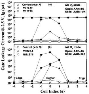
Plasma charging damage in fluorinated and nitrided oxides was investigated. Metal antenna structures attached to the gate with various antenna area ratios (AAR) were used to monitor the plasma charging damage. Previously, I we have demonstrated that severe
charg@g damage could occur at the wafer center for nMOS devices, due to the non-uniform plasma generation caused by the gas injection mode of the asher [7]. Figure 3 shows gate leakage current as a function of cell position for FS samples (Fig. 3a) and FG samples
(Fig. 3b) with various AAR. It can be seen that fluorinated oxides depict reduced plasma-induced leakage current, compared to the controls with pure oxide. The improvement appears to be larger at a medium dose (- 1E14 cm-’). In addition, FG implant appears to be more effective than FS implant.
Such phenomena can be attributed to fluorine
incorporation into gate oxide. The structure relaxation of the stress/strain Si02 by F atoms terminating Si dangling bonds and replacing weak Si-H bonds can substantially improve the GOI. Since it has been speculated that trap creation mechanism responsible for stress-induced
leakage current (SILC) is hydrogen-related, the
incorporated fluorine is expected to replace the weak Si-
H (3.18 ev) bond with strong Si-F bond (5.73 eV) [SI. As a result, gate leakage current after plasma charging can be reduced. This can be accomplished by appropriate amount of F incorporation. Nevertheless, excess fluorine is also known to deteriorate GO1 by creating trap charge in the bulk oxide as well as at the interface, explaining why a medium dose yields a better improvement. Since substrate implant is expected to incorporate more amount of implanted atoms into oxide, this explains why
FG samples are even less leaky than FS samples.
Figure 4 shows the counterparts of Fig. 3 for NS
samples (Fig. 4a) and NG samples (Fig. 4b). It can be
seen that nitrogen implant is much more effective in
suppressing gate leakage current than fluorine
counterparts. In fact, only slight increase in gate current is observed for large-AAR devices with N S l E l 4 . Unlike
fluorine implant, however, plasma-induced leakage current of NS seems to be more effectively suppressed
than that of NG, even though the Tox of NS samples is
thinner than that of NG samples. This is probably
because the optimized dose for nitrogen incorporation into oxide is larger than that for fluorine. It is worthy to note that large tunneling current of N S l E l S samples
occurs and masks the plaspa-induced leakage current due to Tox thinning to 22A, and gate leakage current loses its sensitivity to detect charging damage.
We have also investigated the charging damage induced in fluorine- and nitrogen-implanted N20- nitrided oxide. Since N 2 0 oxide used in this study has been previously shown as genuinely robust to charging damage [7], our focus is on further improving the plasma charging immunity. As shown in Fig.5, gate leakage current is effectively suppressed in F S l E l 4 samples
with nitrided oxide. However, for NG and NS samples
with N20 oxide, unexpected large leakage current is observed (results not shown), which is even worse than
that of N20 control samples without any F or N implantation. This can be ascribed to sufficient nitrogen incorporation in N 2 0 control samples already. Further nitrogen implant only causes excess nitrogen and in turn degrades oxide reliability. Therefore, GO1 of N20 oxide is expected to be improved by simply incorporating fluorine.
111. Improved Gate Oxide Integrity in PMOS with Fluorine Implant
Finally, the effects of fluorine implant on PMOS GO1 was analyzed. As shown in Fig. 6, we found that negligible boron penetration is induced with F G l E l 4
samples since the flat-band voltages of F G l E l 4 samples
and the boron-implanted control samples are almost identical (-1 volt). However, samples with FGlElS and
BF2-implant depict large flat-band voltage shift, due to the well-known fluorine-enhanced boron penetration effects. To confirm this point, gate oxide reliability was analyzed by charge-to-breakdown (Qbd) measurements, as shown in Fig. 7. Significant improvement in Qbd characteristics is observed for F G l E l l samples. In
addition to improve Qbd value, the tail distribution is
also drastically reduced. These findings, although not previously reported on PMOS devices, can be explained consistently with previous literature report on nMOS devices [5]. The improvement in Qbd distribution tail is ascribed to F incorporation, which serves to reduce the local defects that cause the random failure, similar to nMOS case. Finally, plasma charging damage in PMOS with fluorinated oxides is analyzed and shown in Fig. 8. In contrast to the control samples without F incorporation, the leakage current characteristics of antenna devices of FGlEl4 samples are significantly
improved. Such phenomena can also be explained by proper F incorporation in the oxide. Therefore, GO1 integrity can be significantly improved in nMOS as well as in PMOS devices with medium-dose fluorine implant, making this technique suitable for CMOS device application.
CONCLUSION
We have studied the effects of fluorine and nitrogen incorporation into poly gate and Si substrate on ultra-thin gate oxide integrity (GOI). The clever manipulation of fluorine (to increase Tox) and nitrogen (to decrease Tox) implantation into Si substrate prior to oxidation can be used to obtain multiple oxide thickness on the wafer, albeit its effectiveness is significantly reduced for N20 oxide, due to the retardation nature of nitrogen. More importantly, we also found that charging damage in devices with pure oxide can be effectively reduced by proper dose of fluorine and nitrogen implantation. In addition, since sufficient nitrogen is already present in N20 oxide, fluorine-alone implant is essential for GO1 improvement. Finally, we have demonstrated for the first time that CMOS GO1 improvement can actually be accomplished with medium-dose fluorine implantation, even for PMOS devices without showing noticeable enhancement of boron penetration.
ACKNOWLEDGMENT
The authors would like to thank the staff of National Nan0 Device Laboratories for their technical assistance during the course. This work was supported by the National Science Council of the Republic of China under contract No. NSC-89-2215-E-3 17-002.
4.0 3.8
REFERENCES
[ 11 C. T. Liu, et al., ZEDM Tech. Dig., p.499 (1 996). [2] L. K. Han, et al., ZEDM Tech. Dig., p.643 (1997). [3] Y. Nishioka, etal., IEEEYEDL, p. 141 (1989). [4] M. Ushiyama, et al., VLSI Tech Dig., p. 18 (1999). [5] M. Ushiyama, etal., ZEEEARPS, p. 93 (1999). [6] R. Williams, etal., J. Appl. Phys, p. 695 (1975). [7] C.-C. Chen, et al., ZEEDEDL, p. 15 (2000).
[E] I? Chowdhury, et al., Appl, Phys. Lett., p. 37 (1997).
I 0 , O x i d e
P
b
A . 3.8 X 3.6 v5
3.4 v ) . v ) -3.2 X I .g 3.0 h 3.6 c 3.2 x 3.0f
51
'
X 2.6 0 Control.-
- 1 2~ 2'4€
Control I 0 FS A N S 2 . 0 1 . ' ' ' ' ' ' ' ' '.
' ' ' Co nt ro I 1E14 1E15 Implant Dosage ( c m - 2 )Fig. 1 Gate oxide thickness for 0 2 oxides as a function of fluorine or nitrogen dose.
P e
2 . 2 1 " " " I ' " "
Control 1E14 1 E15
Imp la nt Dosage (cm-2)
Fig. 2 Gate oxide thickness for N20 oxides as a
function of fluorine or nitrogen dose.
h 108
2
W 105 Solid AAR-IOKs
103 q4 102g
10'k
v! c a, loo contml(w/oF) (b) FG 0, oxide Open: AAR.16 Solid A A F t l O h Mgr i - 4 - 3 - 2 - 1 0 1 2 3 4cell
Index (#)Fig. 3 Gate current as a function of cell position
for antenna devices with O2 oxides and fluorine implanting into (a) substrate and (b) gate.
NS 0, oxide Open: AAR=I 6 Solid: AAR-1 OK 103 Open: AAR=16 Solid: AAR=IOK - 4 - 3 - 2 - 1 0 1 2 3 4 Cell Index (#)
Fig. 4 Gate current as a function of cell position for
antenna devices with O2 oxides and nitrogen
implanting into (a) substrate and (b) gate.
4 3 - 2 - 1 0 1 2 3 4
Cell Index (#)
Fig. 5 Gate current as a function of cell position for
antenna devices with N20 oxides and with or without fluorine implanting into substrate.
.""
L-
B+FIE14, V,,=I.O-1.5 -1.0 -0.5 0.0 0.5 1.0 1.5 2.0
Gate Voltage (volt)
Fig. 6 High fkequency C-V characteristics of all four splits. Typical flatband voltages are also shown.
J=+O.I A l c m '
".
.
0.1 1 1 0 100
Charge-to-Breakdown (C/cm2)
Fig. 7 Cumulative failure of charge-to-breakdown
(Qbd)
measurement for samples from all four splits.99 h
s
2.5
70h
30'
1 0 A r e a = 2 0 x 2 0 p m 2 U-
A A R = l B , B.-
-
g
50 a-
-
A A R = I B . B + F I E 1 4 --t AAR=IK, B + A A R = I K , B + F l E 1 4 ' ' . . . ' ' ' . . ' . , I ' ' . l l l l " ' ' , - , " " ".'"''' ".."." ' ' . ' . ' , , I '-
10-1 i o 0 io1 i o 2 103 104 105 106 107 108Gate Leakage Current@ Vg=+ZV ( P A )
Fig. 8 Cumulative probabilities of gate leakage
current for PMOS antenna capacitors with and
without medium