IEEE ELECTRON DEVICE LETTERS, VOL. 32, NO. 9, SEPTEMBER 2011 1239
Gate-All-Around Poly-Si TFTs With
Single-Crystal-Like Nanowire Channels
Tsung-Kuei Kang, Ta-Chuan Liao, Chia-Min Lin, Han-Wen Liu, Fang-Hsing Wang, and Huang-Chung Cheng
Abstract—The gate-all-around (GAA) poly-Si thin-film tran-sistors (TFTs) with single-crystal-like nanowire (NW) channels (SCLNCs) are demonstrated and characterized. Via the nanoscale nitride spacer, the Si NW can be easily transformed within one crystalline grain of the two-shot sequential-lateral-solidification poly-Si film. As compared with the planar ones, the GAA-SCLNC TFTs showed more excellent characteristics. The results clearly show that the variations of device characteristics can be reduced by increasing the numbers of NWs in the channels and an average mobility above 410 cm2/V· s with a low standard deviation can
be achieved for the GAA-SCLNC TFTs with 20-NW channels. Index Terms—Field-effect mobility, gate-all-around (GAA), nanowire (NW), nitride spacer, sequential lateral solidification (SLS), single-crystalline-like.
I. INTRODUCTION
T
HE GRAIN boundaries of poly-Si in the channel region seriously affect the carrier transport and device perfor-mance for low-temperature poly-Si (LTPS) thin-film transistors (TFTs). Therefore, enlarging the grains and reducing grain boundaries contained in the channel region are useful methods to improve the performances of LTPS TFTs. Many solid-phase and excimer-laser-crystallization (ELC) approaches that con-vert an as-deposited amorphous Si (a-Si) film into a crystalline Si film have been studied [1]–[3]. Although high-mobility LTPS TFTs have been achieved by the ELC approach, narrow process window and poor uniformity of device performance were exhibited in ELC LTPS TFTs [4], [5]. Based on con-trolled manipulation of the super-lateral-growth phenomenon, the sequential-lateral-solidification (SLS) process can effec-tively produce either directionally solidified microstructure orManuscript received May 24, 2011; accepted June 14, 2011. Date of publication August 17, 2011; date of current version August 24, 2011. This work was supported in part by Alchip Company under Contract 9621071A, by the National Nano Device Laboratories, Taiwan, under Contract NDL C05M2G-023, and by the National Science Council under Grant NSC 98-2218-E-009-010. The review of this letter was arranged by Editor W. T. Ng.
T.-K. Kang and C.-M. Lin are with the Department of Electronic Engineer-ing, Feng Chia University, Taichung 407, Taiwan.
T.-C. Liao is with the Taiwan Semiconductor Manufacturing Company, Hsinchu 300, Taiwan, and also with the Department of Electronics Engineering and the Institute of Electronics, National Chiao Tung University, Hsinchu 300, Taiwan.
H.-W. Liu and F.-H. Wang are with the Department of Electrical Engineering, National Chung Hsing University, Taichung 402, Taiwan.
H.-C. Cheng is with the Department of Electronics Engineering and the Institute of Electronics, National Chiao Tung University, Hsinchu 300, Taiwan. Color versions of one or more of the figures in this letter are available online at http://ieeexplore.ieee.org.
Digital Object Identifier 10.1109/LED.2011.2160146
location-controlled single-crystal-like region on Si films [6]– [8]. An alternative approach to improve device performance is to reduce the total amount of defects by thinning down the channel body. Poly-Si nanowire (NW) TFTs exhibited excellent characteristics [9]–[12]. Previous results clearly indicated the effectiveness of multiple-gated scheme with NW channels in improving the device performance, owing to better gate con-trollability over the channel, resulting in higher performances on Ion, Vth, subthreshold swing (SS), μ, and drain-induced barrier lowering (DIBL) as well [13]–[18]. For most NW fabrication methods, the poor process uniformity would lead to variations of device characteristics [15]. In this letter, the regularly arranged single-crystal-like grains are produced by the SLS process. By scaling down the channel body to be within one single-crystal-like grain and the gate-all-around (GAA)-gated configuration, excellent performance can be expected for the proposed single-crystal-like NW channel (SCLNC) poly-Si TFTs.
II. DEVICEFABRICATION
First, a 50-nm-thick SiN film and a 300-nm-thick tetraethyl orthosilicate (TEOS) oxide were deposited by low-pressure chemical vapor deposition (LPCVD) at 780 ◦C and 700 ◦C on an oxidized substrate. Then, a 40-nm a-Si layer was de-posited by the LPCVD furnace at 550◦C. The two-shot SLS crystallization with 900 mJ/cm2was performed to transfer a-Si into poly-Si with large grains [19]. After a 100-nm-thick TEOS oxide deposition by LPCVD at 700◦C, the oxide was patterned as several dummy strips by standard optical lithography and etched with 100 nm in depth by anisotropic etching to form the step profile. After a 200-nm-thick nitride deposition and a pho-toresist definition for source and drain (S/D) pads, anisotropic etching was performed to form the nitride hard mask for the device active region with NW channels, as shown in Fig. 1(a) and (b). Next, the dummy strips between S/D regions were removed by a diluted HF solution. Then, anisotropic etching of the poly-Si layer led to the formation of the S/D pads and poly-Si NWs in which the wire width was transferred by the size of the nitride spacer in Fig. 1(a). The nitride was removed by hot H3PO4 at 165 ◦C, and the 300-nm TEOS oxide was partially removed by a diluted HF solution. After the etching with HF, the suspending spacer NW channel was braced with S/D pads. The channels were then surrounded by 25-nm-thick TEOS oxide and 200-nm-thick in situ n+-doped poly-Si, and the GAA poly-Si with SCLNC was obtained, as shown in Fig. 1(c). After poly-Si gate patterning, self-aligned phosphorous S/D implantation was performed at 30 keV with a
1240 IEEE ELECTRON DEVICE LETTERS, VOL. 32, NO. 9, SEPTEMBER 2011
Fig. 1. Schematic diagrams of the key fabrication steps for GAA-SCLNC TFTs: (a) SLS process, SiO2dummy strip patterning, nitride deposition, and
the formation of nitride spacer. (b) SEM images of poly-Si film with SLS process after Secco-etching treatment. The left inset shows the top views for S/D nitride pad and nitride spacer. (c) Three-dimensional GAA formation.
dose of 5× 1015cm−2, and a 300-nm-thick passivation oxide layer was deposited by LPCVD at 700◦C. Standard contact opening formation and metallization were carried out. For the purpose of comparison, the conventional planar (CP) poly-Si TFTs were also fabricated with the same process run.
III. RESULTS ANDDISCUSSION
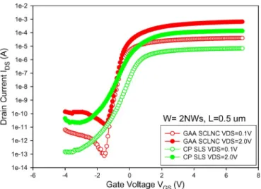
Via the SLS process, the grain boundaries tend to be aligned and lie parallel to the growth direction, and regularly location-controlled irradiated zones (3 μm× 1 μm) can be achieved [5], as shown in Fig. 1(b). Fig. 2 shows the cross-sectional transmission electron microscopy (TEM) image of the fabri-cated GAA-gated structure with SCLNC, good step coverage is observed for the gate oxide and phosphorous in situ doped polygate, and the peripheries of each NW channel are about 28, 28, and 14 nm, respectively. Owing to the small dimension of the nitride spacer, the fabricated NW channel of 14 nm in width can be easily located on the single-crystal-like Si region. The inset in Fig. 2 shows the diffraction pattern of the SCLNC channel. The transfer characteristics of GAA-SCLNC and CP TFTs are compared in Fig. 3. Those devices have a gate length (L) of 0.5 μm and a channel width of 140 nm (= 70 nm× 2), in which the width of TFTs is defined by two NWs with
one-Fig. 2. Cross-sectional TEM image of SCLNC of GAA-SCLNC TFT. The inset shows the diffraction pattern of the SCLNC channel.
Fig. 3. Transfer characteristics of GAA-SCLNC and CP-SLS TFTs with two-NW channels.
Fig. 4. Mean and standard deviation of the mobility for GAA-SCLNC and CP-SLS TFTs. For each device condition, 20 samples were characterized.
dummy-strip structure, as shown in Fig. 3. The Vthwas defined as the gate voltage that is required to obtain a normalized drain current of IDS= (W/L)× 10−8 A at VDS= 0.1 V. SS was
KANG et al.: GATE-ALL-AROUND POLY-Si TFTs WITH SINGLE-CRYSTAL-LIKE NANOWIRE CHANNELS 1241
extracted at VDS= 0.1 V, and the maximum on-current (Ion), the minimum off-current (Ioff), and the maximum on/off-current ratio (Ion/Ioff) were defined at VDS= 2 V. The field-effect mobility was extracted from the peak linear transconduc-tance at VDS= 0.1 V. DIBL was defined as ΔVGS/ΔVDS at
IDS= 10−10 A. Compared to CP TFTs, GAA-SCLNC TFTs show a smaller Vth (from −0.25 to −0.75 V), steeper SS (from 327 to 109 mV/dec), higher on/off-current ratios (from 6.43× 10⁷ to 8.65× 10⁷), higher field-effect mobility (from 208 to 596 cm2/V· s), and higher performance on DIBL (from
0.41 to 0.06 V/V). Most CP TFT devices (width≥ 1 μm) have grain boundaries. The chances that the CP TFT devices are formed within one SLS grain are relatively lower compared with those of NW TFT devices. Owing to the high-crystallinity channels, together with the GAA-gated structure, the proposed GAA-SCLNC TFTs exhibit high-performance characteristics. However, the processes of SLS recrystallization and NW fab-rication lead to large variations of device characteristics for GAA-SCLNC TFTs with two NWs in the channels due to their different grain orientations and intragrain defect distribution among samples. During the SLS process, as the film is cooling, lateral solidification commences from the solid–liquid interface at the boundary between the completely and incompletely molten regions into the molten areas, and such growth leads to single crystal in a zone [6]. In each SLS zone, the crystalline orientation depends on the surviving residual unmelted silicon seeds at the Si bottom [20]. Therefore, each SLS zone exhibits different grain orientations. In this letter, the channels of TFT devices may be located on different SLS Si zones. According to the SEM image in Fig. 1(b), there are chances that the NWs meet with the grain boundaries along the growth direction, and this intragrain defect in the Si channel will degrade the TFT characteristics. Therefore, the deviation of TFT performance is related to different grain orientations and intragrain defect. To exhibit the variation issue, GAA-SCLNC TFTs with varied NW numbers of 2, 4, 10, 20, 30, and 40 were characterized in Fig. 4. Twenty samples of each condition were measured for statistics. It shows that the variation of device performance reduces with increasing NW numbers, which results from the average of the different intrinsic qualities of NWs. In addition, an average mobility above 410 cm2/V· s can be achieved for
the GAA-SCLNC TFTs with 20-NW channels, which is much higher than 190 cm2/V· s for CP TFTs.
IV. CONCLUSION
Via nitride spacer patterning technique, the single-crystalline-like channel in Si NWs much improves the electrical performances of TFT devices. High field-effect mobility above 410 cm2/V· s with a low standard deviation
has been achieved. This work reveals that GAA-SCLNC TFTs are highly promising for the system-on-panel applications.
REFERENCES
[1] J. S. Im and R. S. Sposili, “Crystalline Si films for integrated active matrix liquid-crystal displays,” MRS Bull., vol. 21, no. 3, p. 39, 1996.
[2] J. S. Im and H. J. Kim, “Phase transformation mechanisms involved in excimer laser crystallization of amorphous silicon films,” Appl. Phys.
Lett., vol. 63, no. 14, pp. 1969–1971, Oct. 1993.
[3] C. W. Lin, L. J. Cheng, Y. L. Lu, Y. S. Lee, and H. C. Cheng, “High-performance low-temperature poly-Si TFTs by excimer laser irradiation with recessed-channel structure,” IEEE Electron Device Lett., vol. 22, no. 6, pp. 269–271, Jun. 2001.
[4] G. K. Giust, T. W. Sigmon, P. G. Carey, B. Weiss, and G. A. Davis, “Low temperature polysilicon thin-film transistors fabricated from laser-processed sputtered-silicon films,” IEEE Electron Device Lett., vol. 19, no. 9, pp. 343–344, Sep. 1998.
[5] G. K. Giust, T. W. Sigmon, J. B. Boyce, and J. Ho, “High-performance laser-processed polysilicon thin-film transistors,” IEEE Electron Device
Lett., vol. 20, no. 2, pp. 77–79, Feb. 1999.
[6] R. S. Sposili and J. S. Lm, “Sequential lateral solidification of thin sil-icon films on SiO2,” Appl. Phys. Lett., vol. 69, no. 19, pp. 2864–2866,
Nov. 1996.
[7] J. S. Im, R. S. Sposili, and M. A. Crowder, “Single crystal Si films for thin film transistor devices,” Appl. Phys. Lett., vol. 70, no. 25, pp. 3434–3436, Jun. 1997.
[8] M. A. Crowder, P. G. Carey, P. M. Smith, R. S. Sposili, H. S. Cho, and J. S. Im, “Low-temperature single-crystal Si TFTs fabricated on Si films processed via sequential lateral solidification,” IEEE Electron Device
Lett., vol. 19, no. 18, pp. 306–308, Aug. 1998.
[9] T. C. Liao, S. W. Tu, M. H. Yu, W. K. Lin, C. C. Liu, K. J. Chang, Y. H. Tai, and H. C. Cheng, “Novel gate-all-around poly-Si TFTs with multiple nanowire channels,” IEEE Electron Device Lett., vol. 29, no. 8, pp. 889–891, Aug. 2008.
[10] M. Im, J. W. Han, H. Lee, L. E. Yu, S. Kim, S. C. Jeon, K. H. Kim, G. S. Lee, J. S. Oh, Y. C. Park, H. M. Lee, and Y. K. Choi, “Multiple-gate CMOS thin-film transistor with polysilicon nanowire,” IEEE Electron
Device Lett., vol. 29, no. 1, pp. 102–105, Jan. 2008.
[11] H. Yin, W. Xianyu, A. Tikhonovsky, and Y. S. Park, “Scalable 3-D fin-like poly-Si TFT and its nonvolatile memory application,” IEEE Trans.
Electron Devices, vol. 55, no. 2, pp. 578–584, Feb. 2008.
[12] H. C. Lin, H. H. Hsu, C. J. Su, and T. Y. Huang, “A novel multiple-gate polycrystalline silicon nanowire transistor featuring an inverse-T gate,”
IEEE Electron Device Lett., vol. 29, no. 7, pp. 718–720, Jul. 2008.
[13] H. Takato, K. Sunouchi, N. Okabe, A. Nitayama, K. Hieda, F. Horiguchi, and F. Masuoka, “Impact of surrounding gate transistor (SGT) for ultra-high-density LSIs,” IEEE Trans. Electron Devices, vol. 38, no. 3, pp. 573– 578, Mar. 1991.
[14] C. P. Auth and J. D. Plummer, “Scaling theory for cylindrical, fully-depleted, surrounding-gate MOSFETs,” IEEE Electron Device Lett., vol. 18, no. 2, pp. 74–76, Feb. 1997.
[15] H. H. Hsu, T. W. Liu, L. Chan, C. D. Lin, T. Y. Huang, and H. C. Lin, “Fabrication and characterization of multiple-gated poly-Si nanowire thin-film transistors and impacts of multiple-gate structures on device fluctuations,” IEEE Trans. Electron Devices, vol. 55, no. 11, pp. 3063–3069, Nov. 2008.
[16] B. Doyle, B. Boyanov, S. Datta, M. Doczy, S. Hareland, B. Jin, J. Kavalieros, T. Linton, R. Rios, and R. Chau, “Tri-gate fully-depleted CMOS transistors: Fabrication, design and layout,” in VLSI Symp. Tech.
Dig., 2003, pp. 133–134.
[17] P. Sallagoity, M. Ada-Hanifi, M. Paoli, and M. Haond, “Analysis of width edge effects in advanced isolation schemes for deep submicron CMOS technologies,” IEEE Trans. Electron Devices, vol. 43, no. 11, pp. 1900– 1906, Nov. 1996.
[18] A. Burenkov and J. Lorenz, “Corner effect in double and triple gate Fin-FETs,” in Proc. 33rd ESSDERC, 2003, pp. 135–138.
[19] J. Y. Park, H. H. Park, K. Y. Lee, and H. K. Chung, “Design of sequential solidification crystallization method for low temperature poly-Si thin film transistors,” Jpn. J. Appl. Phys., vol. 43, no. 1, pp. 1280–1286, Apr. 2004. [20] J. S. Im and H. J. Kim, “On the super lateral growth phenomenon observed in excimer laser-induced crystallization of thin Si films,” Appl. Phys. Lett., vol. 64, no. 17, pp. 2303–2305, Apr. 1994.