N A N O E X P R E S S
Open Access
Forming-free bipolar resistive switching in
nonstoichiometric ceria films
Muhammad Ismail
1,3, Chun-Yang Huang
1, Debashis Panda
1, Chung-Jung Hung
2, Tsung-Ling Tsai
1,
Jheng-Hong Jieng
1, Chun-An Lin
1, Umesh Chand
1, Anwar Manzoor Rana
3, Ejaz Ahmed
3, Ijaz Talib
3,
Muhammad Younus Nadeem
3and Tseung-Yuen Tseng
1*Abstract
The mechanism of forming-free bipolar resistive switching in a Zr/CeOx/Pt device was investigated. High-resolution transmission electron microscopy and energy-dispersive spectroscopy analysis indicated the formation of a ZrOy layer at the Zr/CeOxinterface. X-ray diffraction studies of CeOxfilms revealed that they consist of nano-polycrystals embedded in a disordered lattice. The observed resistive switching was suggested to be linked with the formation and rupture of conductive filaments constituted by oxygen vacancies in the CeOxfilm and in the nonstoichiometric ZrOyinterfacial layer. X-ray photoelectron spectroscopy study confirmed the presence of oxygen vacancies in both of the said regions. In the low-resistance ON state, the electrical conduction was found to be of ohmic nature, while the high-resistance OFF state was governed by trap-controlled space charge-limited mechanism. The stable resistive switching behavior and long retention times with an acceptable resistance ratio enable the device for its application in future nonvolatile resistive random access memory (RRAM).
Keywords: Resistive switching; Space charge-limited conduction (SCLC); Metal-insulator-metal structure; Cerium oxide; Oxygen vacancy
Background
A metal-insulator-metal (MIM) structure-based resistive random access memory (RRAM) device has attracted much attention for next-generation high-density and low-cost nonvolatile memory applications due to its long data retention, simple structure, high-density integration, low-power consumption, fast operation speed, high scal-ability, simple constituents, and easy integration with the standard metal oxide semiconductor (MOS) technology [1]. In addition to transition metal oxide-based RRAMs [2,3], many rare-earth metal oxides, such as Lu2O3, Yb2O3,
Sm2O3, Gd2O3, Tm2O3, Er2O3, Nd2O3, Dy2O3, and CeO2
[4-10], show very good resistive switching (RS) properties. Among them, CeO2 thin films having a strong ability
of oxygen ion or oxygen vacancy migration attract a lot of attention for RRAM applications [8-10]. CeO2is a
well-known rare-earth metal oxide with a high dielectric constant (26), large bandgap (6 eV), and high refractive
index (2.2 to 2.3). The cerium ion in the CeO2film exhibits
both +3 and +4 oxidation states, which are suitable for valency change switching process [11,12]. Forming-free resistive switching and its conduction mechanism are very important for nonvolatile memory applications. In addition, oxygen vacancies or ions play a unique role in the resistive switching phenomenon [13]. Therefore, CeO2 is
expected to have potentials for applications in nonvolatile resistive switching memory devices [14]. However, there are quite limited reports on the resistive switching proper-ties of CeO2.
Here, we report the forming-free bipolar resistive switching properties of a nonstoichiometric CeOx film having a Zr/CeOx/Pt device structure. The effect of the Zr top electrode on the resistive switching behavior of the CeOx film is investigated. It is expected that the Zr top electrode reacts with the CeOx layer and forms an interfacial ZrOylayer. This reaction may be responsible for creating a sufficient amount of oxygen vacancies re-quired for the formation and rupture of conductive fila-ments for resistive switching. In this study, we have found that the CeOx-based RRAM device exhibits good
* Correspondence:[email protected] 1
Department of Electronics Engineering and Institute of Electronics, National Chiao Tung University, Hsinchu 30010, Taiwan
Full list of author information is available at the end of the article
© 2014 Ismail et al.; licensee Springer. This is an Open Access article distributed under the terms of the Creative Commons Attribution License (http://creativecommons.org/licenses/by/2.0), which permits unrestricted use, distribution, and reproduction in any medium, provided the original work is properly cited.
switching characteristics with reliable endurance and data retention, suitable for future nonvolatile memory applications.
Methods
A 200-nm-thick silicon dioxide (SiO2) layer was
ther-mally grown on a (100)-oriented p-type Si wafer sub-strate. Next, a 50-nm-thick Pt bottom electrode was deposited on a 20-nm-thick Ti layer by electron beam evaporation. The 14- to 25-nm-thick CeOx films were
deposited on Pt/Ti/SiO2/Si at room temperature with a gas
mixture of 6:18 Ar/O2by radio-frequency (rf) magnetron
sputtering using a ceramic CeO2target. Prior to rf
sputter-ing at 10-mTorr pressure and 100-W power, the base pressure of the chamber was achieved at 1.2 × 10⁻⁶Torr. Finally, a 30-nm-thick Zr top electrode (TE) and a 20-nm-thick W TE capping layer were deposited by direct current (DC) sputtering on the CeOx film through
metal shadow masks having 150-μm diameters to form a sandwich MIM structure. The W layer was used to avoid the oxidation of the Zr electrode during testing. Struc-tural and compositional characteristics of the CeOxfilms
were analyzed by X-ray diffraction (XRD; Bede D1, Bede PLC, London, UK) and X-ray photoelectron spectroscopy (XPS; ULVAC-PHI Quantera SXM, ULVAC-PHI, Inc., Kanagawa, Japan) measurements. The film thickness and interfacial reaction between Zr and CeOxwere confirmed
by high-resolution cross-sectional transmission electron microscopy (HRTEM). Elemental presence of deposited layers was investigated by energy-dispersive spectroscopy (EDX). Electrical current–voltage (I-V) measurement was carried out using the Agilent B1500A (Agilent Technologies, Santa Clara, CA, USA) semiconductor analyzer characterization system at room temperature. During electrical tests, bias polarity was defined with reference to the Pt bottom electrode.
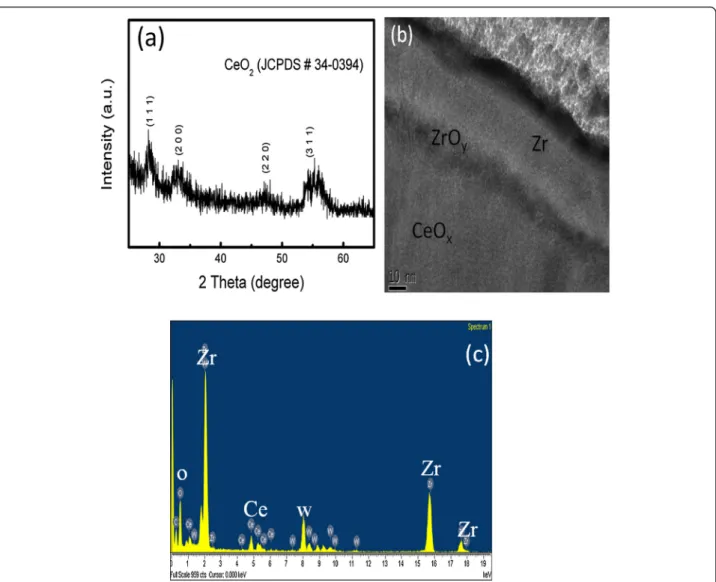
Figure 1 XRD pattern of the CeOxfilm and cross-sectional TEM and EDX images of the Zr/CeOx/Pt device. (a) XRD pattern of the CeOx
Results and discussion
Figure 1a shows the grazing angle (3°) XRD spectra of the CeOxthin film deposited on Si (100) substrate. It
in-dicates that the CeOx film possesses a polycrystalline
structure having (111), (200), (220), and (311) peaks, corresponding to the fluorite cubic structure (JCPDS ref. 34–0394). From the XRD analysis, the broad and wide diffraction peaks demonstrate that the CeOx film
ex-hibits poor crystallization. This could be due to the small thickness (approximately 14 nm) of the film. Figure 1b shows the cross-sectional HRTEM image of the Zr/CeOx/
Pt device, which indicates that the ZrOylayer is formed
be-tween CeOxand Zr interfaces. Figure 1c depicts the EDX
spectra of the CeOx film. The elemental composition
of the Zr/CeOx/Pt was determined by energy dispersion.
The results from the EDX analysis that showed the main component present in this structure were O (38.41%), Zr (34. 05%), and Ce (3.83%). An oxygen peak at about 0.52 keV and Zr peaks at about 22.5 and 15.60 keV can be observed in the spectra.
The ZrOy layer is also observed from XPS signals at
the interface of Zr and CeO2 layers. XPS analysis was
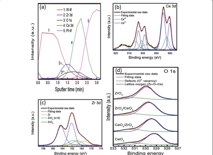
carried out to examine the surface chemical composition and the valence/oxidation states of Ce and Zr species in-volved in the device by inspecting the spectral line shape and signal intensities associated with the core-level elec-trons. Figure 2a shows the depth profile of chemical composition in the Zr/CeOx/Pt device. The interdiffusion
of O, Ce, and Zr atoms are evident from the spectra. This is an indication of the formation of an interfacial ZrOy
layer between the CeOx and Zr top electrode. The
forma-tion of the ZrOylayer is further confirmed from the
shift-ing of Zr 3d peaks from a higher bindshift-ing energy position to lower ones (Figure 2c). The CeOx3d spectrum shown
in Figure 2b consists of two sets of spin-orbit multiplets. These multiplets are the characteristics of 3d3/2and 3d5/2
(represented asu and v, respectively) [15]. The spin-orbit splitting is about 18.4 eV. The highest peaks at around 880.2 and 898.7 eV, recognized as v0and u0respectively,
correspond to Ce3+ with the highest satellites as v′
Figure 2 XPS binding energy profiles. (a) Depth profiles of Zr, Ce, O, Pt, and W for the W/Zr/CeOx/Pt structure, (b) Ce 3d, (c) Zr 3d, and
(885.1 eV) and u′ (903.3 eV). Low-intensity peaks, i.e., v (882.5 eV) and u (900.9 eV) along with satellite features represented asv″ (889.4 eV), v‴ (897.5 eV), u″ (905.4 eV), and u‴ (914.6 eV), are observed, corresponding to the Ce4+state.
In reference to the differentiation between the Ce3+and Ce4+ species with different line shapes, the XPS spectra correspond to various final states: Ce(III) =v0+v′ + u0+u′
and Ce(IV) =v + v″ + v‴ + u + u″ + u‴ [16]. The presence of the Ce4+state is normally supported by the intensity of the u‴ peak, which is known as a fingerprint of Ce(IV) states [16]. This result implies that both Ce4+and Ce3+ions coexist in the bulk as well as in the surface of the CeOx
film. Concentrations of Ce4+ and Ce3+, as obtained from the deconvoluted XPS spectra, are 39.6% and 60.4%, re-spectively. The higher percentage of Ce3+ ions indicates that the film is rich of oxygen vacancies [17]. The XPS spectra of Zr 3d exhibit a doublet located at 184.3 and
182.08 eV, as shown in Figure 2c. This doublet corresponds to Zr 3d3/2and Zr 3d5/2, respectively [18], as the final states
of ZrO2. Furthermore, the weak bands at about 181.7 eV
assigned to Zr 3d3/2and 180.8 eV assigned to Zr 3d5/2seem
to be consistent with the states of ZrOy (0 <y < 2,
181.6 eV) [19], which also provide an evidence of the for-mation of a ZrOyinterfacial layer. Final states of the
metal-lic Zr (3d) are evidenced by the weakest band at 181.2 eV for Zr 3d3/2and 179.5 eV for Zr 3d5/2. Figure 2d displays
the O 1 s XPS spectra of the Zr/CeOx/Pt device consisting
of peaks at binding energies 529.05, 530.09, and 531.47 eV, which can be attributed to the absorbed oxygen [20], lattice oxygen in CeO2[21], and oxygen vacancies [22],
respect-ively. The O 1 s peak is broad due to the nonequivalence of surface O2–ions. In addition to the oxygen vacancies, the preexisting oxygen ions in the Zr/CeOx/Pt device can
also be verified from the spectra. The presence of more than one peak in the O 1 s spectra may have resulted from
Figure 3 Schematic of oxygen vacancy-formed multiconducting filaments depicting the switching process in Zr/CeOx/Pt device.
(a) Initial, (b) reset, and (c) set states. Note that unfilled (filled) circles represent oxygen vacancies (ions) in the CeOxfilms.
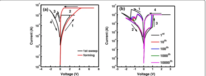
-4 -2 0 2 4 6 8 10-8 10-7 10-6 10-5 10-4 10-3 10-2 Current (A) Voltage (V) 1st sweep forming (a) 1 2 3 4 -3 -2 -1 0 1 2 3 10-9 10-8 10-7 10-6 10-5 10-4 10-3 10-2 Current (A) Voltage (V) 1st 10th 100th 1000th 10000th 1 2 3 4 (b)
Figure 4 Typical bipolar (I-V) curves of resistive switching behavior in Zr/CeOx/Pt devices with different CeOxlayer thicknesses.
the overlapping of oxygen from surface defects (the nonlat-tice oxygen ions), CeOx, and Zr-O-Ce components as
evi-dent from the deconvoluted curves. The deconvoluted peaks detected at 529.2 to 529.9 and 531.47 eV are ascribed to the lattice oxygen and surface defects, respectively. Non-lattice oxygen ions may exist in the grain boundaries and can move with the help of bias voltage. Interaction be-tween the movable oxygen vacancies and oxygen ions in the presence of an external electric field can play an im-portant role in the RS process [23,24]. Based on the above results, a highly stable and forming-free bipolar resistive switching model can be proposed as shown in Figure 3.
Figure 4a depictsI-V bipolar switching characteristics of the Zr/CeOx/Pt device having a CeOx film thickness
of 25 nm under DC sweeping at room temperature. Application of positive DC sweeping voltage gradually activates the device, initially forming a conductive path;
this process is known as‘electroforming’ and is similar to defect-induced dielectric soft breakdown. Current grad-ually increases at the forming voltage (approximately 4 V), and the device is shifted from a high-resistance state (HRS) to a low-resistance state (LRS). At the nega-tive bias of approximately −1.0 V, the current drops abruptly to switch the device from LRS to HRS, known as the reset process. The device returns again to LRS when positive bias exceeds the set voltage (Von~ 2.0 V),
and a compliance current of 10 mA is applied to prevent the device from permanent breakdown. The electroform-ing process usually requires a higher bias and may cause unstable resistance states [8], which make RS characteris-tics very difficult to modulate. That is why it is valuable to study the resistive switching behavior free from the forming process. In this regard, the thickness of the CeOx
layer was reduced from 25 to 14 nm in the Zr/CeOx/Pt
devices. It is noticed that by reducing the thickness of the CeOx layer, the forming voltage is also reduced. At
14-nm-thick CeOx, the Zr/CeOx/Pt device shows a
forming-free behavior, as indicated in Figure 4b. Figure 4b shows the first switching cycle of this device. Initially, the device is in LRS [21], so the first reset process (Voff=−1.4 V) is
required to initialize the device by rupturing the pre-formed conductive filaments between two electrodes, and the device is switched to HRS [22]. A unique resistive switching behavior can be obtained without any forming process, which is more advantageous for the application point of view [2,22]. Conversely, a positive voltage (Von)
of about +1 V is required for the rapid transition of current from HRS to LRS, called the‘set process.’ During the set process, oxygen vacancies migrate from the top reservoir (ZrOy layer) and form conducting filaments
[2,4,13,20]. A compliance current of 1 mA was applied to prevent the device from permanent breakdown. An appro-priate negative voltage (−0.7 V) is applied to switch the device from LRS back to HRS. During the reset process,
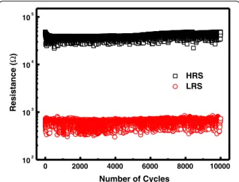
0 2000 4000 6000 8000 10000 102 103 104 105 HRS LRS Resistance ( Ω ) Number of Cycles
Figure 5 Endurance characteristic of the Zr/CeOx/Pt device
during DC sweeping modes up to 104cycles. The read voltage
is 0.3 V. 102 103 104 105 0.5 2 10 30 50 70 90 98 99.5 Cum ulative Pr obability (%) Resistance (Ω) HRS LRS Read @ 0.3 V (a) -2.0 -1.5 -1.0 -0.5 0.0 0.5 1.0 1.5 2.0 2.5 0.5 2 10 30 50 70 90 98 99.5 Cum ulative Pr obability (%) Vreset Vset Voltage (V) (b)
Figure 6 Statistical and probability distributions. (a) Statistical distributions of the HRS and LRS measured during switching up to 104cycles
the conductive filament is ruptured by the reoxidation of oxygen ions [2,13,22,25].
To evaluate the memory switching performance of the Zr/CeOx/Pt device, endurance characteristics are
performed. The memory cell is switched successfully in consecutive 104 switching cycles (I-V curves) with ap-proximately 40 resistance ratios between HRS and LRS, as shown in Figure 5. Both HRS and LRS are quite stable and no ‘set fail’ phenomena are observed. Figure 6a shows the statistical distribution of LRS and HRS of the device. Furthermore, the device has very good uniformity of resistance values in both HRS and LRS. Figure 6b de-picts the distribution of set (Vset) and reset (Vreset)
volt-ages for the device, which shows a narrow range ofVreset
(from −0.5 to −1 V) and Vset(from 0.5 to 1.3 V) values.
The data retention characteristics of the Zr/CeOx/Pt
de-vice are measured at room temperature (RT) and at 85°C, respectively. As shown in Figure 7a, the HRS and LRS
are retained stable for more than 104 s at RT and 85°C with a resistance ratio of approximately 102 times at 0.3 V. Hence, suitable read/write durability is obtained. The nondestructive readout property is also verified. As shown in Figure 7b, the two resistance states are stable over 104s under 0.3 V at RT and 85°C, without any ob-servable degradation.
The RS characteristics of the Zr/CeOx/Pt device are
well explained by the model of filamentary conduction mechanism caused by oxygen ions/vacancies [20,26,27]. Due to impulsive interactions, oxygen vacancies tend to distribute themselves in line patterns and separate from each other in the CeOxfilm [28]. This phenomenon leads
to the formation of independent conducting filaments be-tween electrodes instead of their interconnection network. The abundant oxygen vacancies easily form conducting fil-aments presented in the CeOxfilm, as shown in Figure 3a.
The formation mechanism of the conducting filament in
100 101 102 103 104 10-5 10-4 10-3 [email protected] (A) Retention Time (S) 25 0C 25 0C 85 0C 85 0C (a) 100 101 102 103 104 10-5 10-4 10-3 10-2 Current @0.3V (A) Stress Time (S) HRS @ 250 C LRS @ 250 C HRS @ 850C LRS @ 850 C (b)
Figure 7 Retention characteristic and nondestructive readout properties. (a) Retention characteristic of the Zr/CeOx/Pt device. The
resistance ratios between HRS/LRS are retained for more than 104s. (b) Nondestructive readout properties of both HRS and LRS for 104s.
10-1 100 10-6 10-5 10-4 10-3 10-2 Current (A) Voltage (V) Ohmic Slope = 0.98 Slope = 1.50 Slope = 2.30 reset (a) 10-1 100 10-5 10-4 10-3 Current (A) Voltage (V) Ohmic
Slope = 1.20 Slope = 1.60Schottky Ohmic
Slope = 0.98
set
(b)
Figure 8I-V curves of the Zr/CeOx/Pt memory device are displayed in double-logarithmic scale. The linear fitting results in both ON state
the virgin device could be explained as follows: the oxygen vacancies present in the virgin device can be imagined to be formed partially during the deposition of the nonstoichiometric (oxygen deficient) CeO2and partially
as a consequence of Zr oxidation. The oxidation of Zr might have increased the concentration of oxygen vacan-cies in the bulk of the sandwiched nonstoichiometric oxide to such an extent that they formed conductive paths through CeOx. These conductive filamentary paths
composed of oxygen vacancies are somewhat stronger than the filaments that are formed in the subsequent ON states, as indicated by a relatively larger reset power needed for the first reset process (Figure 3b). Such con-ducting filaments become a cause for the forming-free behavior of the Zr/CeOx/Pt device. In addition, due to the
nonforming process, the current overshoot phenomenon can be suppressed for the following RS [26]. When a nega-tive voltage (Voff) is applied on the top electrode, current
flows (i.e., the electrons injected from the top electrode) through the conductive filaments that produce local heat-ing at the interface along with the repelled oxygen ions from the ZrOylayer, causing local oxidization of the
fila-ments at the interface between ZrOyand CeOxlayers. This
oxidization causes the rupture of filaments and the switch-ing of the device to HRS [29], as shown in Figure 3b. Figure 3c depicts the set process; the device can switch from HRS to LRS by applying a positive bias voltage on the Zr top electrode, which causes the drift of oxygen va-cancies from the ZrOyinterfacial layer down to CeOxand
the oxygen ions simultaneously upward. The conducting filament consisting of oxygen vacancies is formed. In this RS model, the ZrOyinterfacial layer behaved as an oxygen
reservoir in the device. Besides being an oxygen reservoir, the ZrOyinterfacial layer also acts as an ion barrier [30],
which may lead to the good endurance property of the Zr/ CeOx/Pt structure.
In order to elucidate the conduction mechanisms of the device, the I-V curve is plotted in the double-logarithmic mode, both the positive and negative bias regions, as shown in Figure 8a,b, respectively. The con-duction mechanism being responsible for charge trans-port in the low-voltage region involves ohmic behavior (sincen = 1), but it is different in the medium- and high-voltage regions for the device, where the conduction be-havior can be well described by the space charge-limited current (SCLC) theory [31-36]. Ohmic conduction in LRS is assumed to be caused by the oxygen vacancies which probably provide shallow energy levels below the conduction band edge. The SCLC mechanism is gener-ally observed when the electrode contacts are highly car-rier injecting. Due to the formation of an interfacial ZrOy layer between Zr and CeOx films, the conduction
mechanism in the device behaves according to the SCLC theory since the ZrOylayer is known to provide electron
trapping sites and to control the conductivity by trap-ping and detraptrap-ping.
Conclusions
Resistive switching characteristics of the Zr/CeOx/Pt mem-ory device were demonstrated at room temperature. The conduction mechanisms for low- and high-resistance states are revealed by ohmic behavior and trap-controlled space charge-limited current, respectively. Oxygen vacancies pre-sented in the CeOx film and an interfacial ZrOylayer was formed, as confirmed by XPS and EDX studies. Long re-tention (>104s) at 85°C and good endurance with a mem-ory window of HRS/LRS≥ 40 were observed. This device has high potential for nonvolatile memory applications.
Competing interests
The authors declare that they have no competing interests.
Authors’ contributions
The manuscript was written through the contributions of all authors, MI, CYH, DP, CJH, TLT, JHJ, CAL, UC, AMR, EA, IT, MYN, and TYT. All authors read and approved the final manuscript.
Acknowledgements
The authors acknowledge the financial support by the Higher Education Commission (HEC), Islamabad, Pakistan, under the International Research Support Initiative Program (IRSIP). This work was also supported by the National Science Council, Taiwan, under project NSC 99-2221-E009-166-MY3. Author details
1Department of Electronics Engineering and Institute of Electronics, National Chiao Tung University, Hsinchu 30010, Taiwan.2Department of Materials Science and Engineering, National Chiao Tung University, Hsinchu 30010, Taiwan.3Department of Physics, Bahauddin Zakariya University, Multan 60800, Pakistan.
Received: 10 November 2013 Accepted: 13 January 2014 Published: 27 January 2014
References
1. Tseng TY, Sze SM (Eds): Nonvolatile Memories: Materials, Devices and Applications. Volume 2. Valencia: American Scientific Publishers; 2012:850. 2. Panda D, Tseng TY: Growth, dielectric properties, and memory device
applications of ZrO2thin films. Thin Solid Film 2013, 531:1–20.
3. Panda D, Dhar A, Ray SK: Nonvolatile and unipolar resistive switching characteristics of pulsed ablated NiO films. J Appl Phys 2010, 108:104513. 4. Lin CY, Lee DY, Wang SY, Lin CC, Tseng TY: Reproducible resistive
switching behavior in sputtered CeO2polycrystalline films. Surf Coat
Technol 2009, 203:480–483.
5. Liu KC, Tzeng WH, Chang KM, Chan YC, Kuo CC, Cheng CW: The resistive switching characteristics of a Ti/Gd2O3/Pt RRAM device. Microelect Reliab
2010, 50:670–673.
6. Mondal S, Chen HY, Her JL, Ko FH, Pan TM: Effect of Ti doping concentration on resistive switching behaviors of Yb2O3memory cell. Appl Phys Lett 2012,
101:083506.
7. Huang SY, Chang TC, Chen MC, Chen SC, Lo HP, Huang HC, Gan DS, Sze SM, Tsai MJ: Resistive switching characteristics of Sm2O3thin films for nonvolatile
memory applications. Solid State Electron 2011, 63:189–191.
8. Pan TM, Lu CH: Switching behavior in rare-earth films fabricated in full room temperature. IEEE Trans Electron Devices 2012, 59:956–961. 9. Li JGT, Wang Y, Mori T: Reactive ceria nanopowders via carbonate
precipitation. J Am Ceram Soc 2002, 85:2376–2378.
10. Zhou Q, Zhai J: Study of the resistive switching characteristics and mechanisms of Pt/CeOx/TiN structure for RRAM applications. Integr Ferroelectr 2012, 140:16–22.
11. Panda D, Dhar A, Ray SK: Non-volatile memristive switching characteristics of TiO2films embedded with nickel nanocrystals. IEEE
Trans Nanotechnol 2012, 11:51–55.
12. Waser R, Aono M: Nanoionics-based resistive switching memories. Nat Mater 2007, 6:833–840.
13. Panda D, Huang CY, Tseng TY: Resistive switching characteristics of nickel silicide layer embedded HfO2film. Appl Phys Lett 2012, 100:112901.
14. Kano S, Dou C, Hadi MS, Kakushima K, Ahmet P, Nishiyama A, Suggi N, Tsutsui K, Kattaoka Y, Natori K, Miranda E, Hattori T, Iwai H: Influence of electrode materials on CeOxbased resistive switching. ECS Trans 2012, 44:439–443.
15. Rao RG, Kaspar J, Meriani S, Monte R, Graziani M: NO decomposition over partially reduced metallized CeO2-ZrO2solid solutions. Catal Lett 1994,
24:107–112.
16. Bêche E, Charvin P, Perarnau D, Abanades S, Flamant G: Ce 3d XPS investigation of cerium oxides and mixed cerium oxide (CexTiyOz). Surf Inter Anal 2008, 40:264–267.
17. Dittmar A, Hoang DL, Martin A: TPR and XPS characterization of chromia– lanthana–zirconia catalyst prepared by impregnation and microwave plasma enhanced chemical vapour deposition methods. Thermochim Acta 2008, 47:40–46.
18. Meng F, Zhang C, Bo Q, Zhang Q: Hydrothermal synthesis and room-temperature ferromagnetism of CeO2nanocolumns. Mater Lett 2013,
99:5–7.
19. Balatti S, Larentis S, Gilmer DC, Lelmini D: Multiple memory states in resistive switching devices through controlled size and orientation of the conductive filament. Adv Mater 2013, 25:1474–1478.
20. Wang SY, Lee DY, Huang TY, Wu JW, Tseng TY: Controllable oxygen vacancies to enhance resistive switching performance in a ZrO2-based
RRAM with embedded Mo layer. Nanotechnol 2010, 21:495201.
21. Geetika K, Pankaj M, Ram SK: Forming free resistive switching in graphene oxide thin film for thermally stable nonvolatile memory applications. J Appl Phys 2013, 114:124508.
22. Cao X, Li X, Gao X, Yu W, Liu X, Zhang Y, Chen L, Cheng X: Forming-free colossal resistive switching effect in rare-earth-oxide Gd2O3films for
memristor applications. Appl Phys Lett 2009, 106:073723. 23. Kinoshita K, Tamura T, Aoki M, Sugiyama Y, Tanaka H: Bias polarity
dependent data retention of resistive random access memory consisting of binary transition metal oxide. Appl Phys Lett 2006, 89:03509.
24. Janousch M, Meijer GI, Staub U, Delley B, Karg SF, Andreasson BP: Role of oxygen vacancies in Cr-doped SrTiO3for resistance-change memory.
Adv Mater 2007, 19:2232.
25. Panda D, Dhar A, Ray SK: Nonvolatile and unipolar resistive switching characteristics of pulsed laser ablated NiO films. Appl Phys Lett 2011, 108:104513.
26. Lin CY, Wang SY, Lee DY, Tseng TY: Electrical properties and fatigue behaviors of ZrO2resistive switching thin films. J Electrochem Soc 2008,
155:H615–H619.
27. Lin CY, Wang SY, Lee DY, Tseng TY: Ti-induced recovery phenomenon of resistive switching in ZrO2thin films. J Electrochem Soc 2010,
157:G167–G169.
28. Esch F, Fabris S, Zhou L, Montini T, Africh C, Fornasiero P, Comelli G, Rosei R: Electron localization determines defect formation on ceria substrates. Science 2005, 309:752–755.
29. Chen MC, Chang TC, Huang SY, Chen SC, Hu CW, Tsai CT, Sze M: Bipolar resistive switching characteristics of transparent indium gallium zinc oxide resistive random access memory. Electrochem Solid State Lett 2010, 13:H191–H193.
30. Chang WY, Ho YT, Hsu TC, Chen F, Tsai MJ, Wu TB: Influence of crystalline constituent on resistive switching properties of TiO2memory films.
Eletrochem Soild-State Lett 2009, 12:H135–H137.
31. Liu Q, Guan W, Long S, Jia R, Liu M, Chen J: Resistive switching memory effect of ZrO2films with Zr+implanted. J Appl Phys 2008,
92:012117.
32. Guan W, Long S, Liu Q, Liu M, Wang W: Nonpolar non-volatile resistive switching in Cu doped ZrO2. IEEE Trans Elec Lett 2008, 29:434–437.
33. Liu Q, Long S, Wang W, Zuo Q, Zhang S, Chen J, Liu M: Improvement of resistive switching properties in ZrO2-based RRAM with implanted Ti
ions. IEEE Trans Elec Lett 2009, 30:1335–1337.
34. Long S, Cagli C, Lelmini D, Liu M, Sune J: Analysis and modeling of resistive switching characteristics. J Appl Phys 2012, 111:074508.
35. Long S, Cagli C, Lelmini D, Liu M, Sune J: Reset statistics of NiO-based resistive switching memory. IEEE Trans Elec Lett 2011, 32:1570–1572.
36. Long S, Cagli C, Lelmini D, Liu M, Sune J: A model for the set statistics of RRAM inspired in the percolation model of oxide breakdown. IEEE Trans Elec Lett 2013, 34:999–1001.
doi:10.1186/1556-276X-9-45
Cite this article as: Ismail et al.: Forming-free bipolar resistive switching in nonstoichiometric ceria films. Nanoscale Research Letters 2014 9:45.
Submit your manuscript to a
journal and benefi t from:
7 Convenient online submission 7 Rigorous peer review
7 Immediate publication on acceptance 7 Open access: articles freely available online 7 High visibility within the fi eld
7 Retaining the copyright to your article