行政院國家科學委員會專題研究計畫 成果報告
非晶矽薄膜電晶體作為光感測元件及電路之研究(II)
研究成果報告(精簡版)
計 畫 類 別 : 個別型 計 畫 編 號 : NSC 99-2221-E-009-121- 執 行 期 間 : 99 年 08 月 01 日至 100 年 07 月 31 日 執 行 單 位 : 國立交通大學光電工程學系(所) 計 畫 主 持 人 : 戴亞翔 計畫參與人員: 碩士班研究生-兼任助理人員:李政哲 碩士班研究生-兼任助理人員:盧冠銘 碩士班研究生-兼任助理人員:林寬達 博士班研究生-兼任助理人員:周祿盛 報 告 附 件 : 出席國際會議研究心得報告及發表論文 處 理 方 式 : 本計畫涉及專利或其他智慧財產權,2 年後可公開查詢中 華 民 國 100 年 10 月 26 日
1
行政院國家科學委員會補助專題研究計畫
成果報告
□期中進度報告
非晶矽薄膜電晶體作為光感測元件及電路之研究(II)
計畫類別:個別型計畫 □整合型計畫
計畫編號:NSC
99
-
2221
-
E
-
009
-121
執行期間: 99 年 8 月 1 日至 100 年 7 月 31 日
執行機構及系所:交通大學 光電工程學系(所)
計畫主持人:戴亞翔 副教授
共同主持人:
計畫參與人員:周祿盛、盧冠銘、李政哲、林寬達
成果報告類型(依經費核定清單規定繳交):精簡報告 □完整報告
本計畫除繳交成果報告外,另須繳交以下出國心得報告:
□赴國外出差或研習心得報告
□赴大陸地區出差或研習心得報告
出席國際學術會議心得報告
□國際合作研究計畫國外研究報告
處理方式:
除列管計畫及下列情形者外,得立即公開查詢
涉及專利或其他智慧財產權,□一年二年後可公開查詢
中 華 民 國 100 年 10 月 26 日
2 (一)
中、英文摘要及關鍵詞
(keywords)
關鍵詞:薄膜電晶體, 感光效應, 偵測器 非晶矽薄膜電晶體由於它的高光感測性以及較易製作於大面積上,在主動矩陣液晶顯示器以 及偵測器上受到廣泛的注意。之前的研究指出,ㄧ些使用薄膜電晶體的感測機構都已經被論証討 論。然而,大部分傳統型的光感測器都是用外部的分離元件去裝置的,所以會造成額外的成本與 設計上的複雜度。 為了研究上述的這個課題,增加畫素開關薄膜電晶體的速度與光電晶體的動態偵測範圍。在 本計畫中,我們設計多種類型的薄膜電晶體元件,藉由不同結構亦或閘極電壓的調整,我們可以 依照需求決定光產生電流的效率區域多寡。同時,所設計的光電晶體在不同操作區域的不同偵測 能力的特性可被用做動態偵測範圍中提升訊號雜訊的比值。在兩年的計畫中,我們開發了顯示器 的背光感測與正光感測電路,並解決在實際應用上所會遇到的問題。由於整個製程並沒有額外的 流程,這對我們要將光感測器整合是相當有幫助的。同時,我們希望藉由計畫的執行能達到卓越 的研究成果,能更提昇我國技術水準,趕上世界的技術水平,衍生更具附加價值的面板產品。 Keywords:Thin-Film Transistor, Photosensitive effect, SensorHydrogenated amorphous silicon thin film transistors (a-Si:H TFTs) receive extensive application in active matrix liquid crystal display (LCD) and sensors due to its high photo sensitivity and ease of deposition across large area substrates. It was reported that some sensing functions using TFTs were already also demonstrated. However, most of the conventional ambient light sensor systems were implemented by external discrete devices which cause additional cost and the design complexity.
In addition to the research for issues above, to increase the speed of pixel switching TFT, cause a large drop in the dynamic range of photo transistor. In this project, we design some kinds of different type TFT devices. We can make an alteration depletion length to control effective region of photo-excited leakage current from adjustment of different type device structures or gate voltages. Meanwhile, the difference sensing capability of designed photo transistor from the dark to the bright region by itself is adaptive to increase signal-to-noise ratio (SNR) for wide dynamic range. During the past two years, we had developed the front-light sensing and backlight sensing circuits and solved the practical problems when they are applied into TFT LCD. This method does not need novel device process development and can be implemented on to panel helpfully. Furthermore, based on the achievements in these projects, we will help the panel industry in Taiwan to catch up the world.
(二)
報告內容
1. 研究計畫之背景、目的及重要性: 近年來,隨著大尺寸液晶顯示器技術的演進,由小尺寸的 PDA 到數位電視更是蓬勃發展, 在現階段 TFT-LCD 應用產品中,因為較容易沉積實現基板的大型化,而使非晶矽薄膜電晶體為 發展上的主流技術。而又由於隨著平面顯示器逐漸地普及化,對顯示器產品的需求也越來越高, 其中不單只需要顯示功能,非晶矽薄膜電晶體有較高的光敏感性(Photo-Sensitivity),在整合光偵 測器的研究上,非晶矽薄膜電晶體越來越被受到重視。目前改善非晶矽薄膜電晶體的特性及具有 系統性之元件的開發上主要分成二個方面。一是進一步改善平面顯示器的既有特性,加強發揮平 面顯示面板的優勢;二是增加產品的功能整合度,擴張其應用範圍。在特性改善部份,分為液晶 光電特性與高光效率面板光源進行。在功能整合部份,則由製程技術控制,新型元件研究,以及 內建電路和驅動設計著手。圖(一)所示為應用非晶矽薄膜電晶體技術製作之系統整合型顯示面板 示意圖。 本計畫的主要目標,即是發展一種新穎的非晶矽薄膜電晶體元件技術,製作同時兼具高光感 測電流及多功效能的顯示偵測元件。藉由製備與舊有製程上相容的非晶矽薄膜電晶體元件結構, 來提高光敏感性。再利用不同操作區域對應的高光敏感性元件特性的結果設計新型自我調變 (Novel Self-Modulated)的光感測電路,達到多功的 High Dynamic Range 光偵測電路。同時,由於3
現在的面板趨向採用Adaptive Dimming of LED Back Light 的技術(背光源會跟著畫面的明暗做調
變以省功率),發展綠色節能顯示技術 (Green Eco-Display Technology)如圖(二)所示。利用
Partial-Floating-Gate 型的非晶矽薄膜電晶體元件做正照與背照光的光感測系統就相當重要,且藉 由此系統,亦可偵測背光板各個LED 的使用狀況。 其重要性係省去光偵測器於平面顯示器的額外製程條件(如 PIN 二極體中之 p-type 製程),增 加產品的功能整合度,擴張像人機介面亦或 LED 等的應用範圍,以提高平面顯示面板的附加價 值,由於各種顯示元件的結構與製程皆相同,將可使得製作過程單一化,具有極大的技術相容性 與整合性,因此可實現多功能系統整合型顯示面板的目標。計劃目標將完成「建立非晶矽薄膜電
晶體的Sensing System on Panel 的內建電路設計技術。」
[圖一]整合型顯示面板示意圖。[圖二] Adaptive Dimming of LED Back Light 的技術(背光源會 跟著畫面的明暗做調變以省功率)示意圖。 2.國內外有關本計畫之研究情況、重要參考文獻之評述: 以下先就本計畫的相關國內外主要重心加以說明以及重要參考文獻的評述。非晶矽薄膜電晶 體作為光偵測器元件這方面有非常多論文探討[1~15],大多是製作 PIN 二極體之類的元件於製程 條件中,然而,此舉常需要引入額外的製程以及複雜的元件結構來改善,造成製造成本的增加以 及電路設計的複雜度,亦或以電路配合製程條件來設計。 [圖三] 照光的線性關係與使用不同大小 [圖四] 設計非晶矽薄膜電晶體 Source-gate 的結 的 PIN 二極體作光偵測。 構用以提高光漏電。
如圖(三)所示為 SID 2008 年【Hyun Sang, Tae Jun Ha, et al., SID Digest of Tech. Papers, pp 716-719 (2008)】中,照光的線性關係與使用不同大小的 PIN 二極體去作光偵測的示意圖。(SID 會議所發表的文章均是光電資訊顯示領域中極為前瞻的研究成果發表)。由此可以看的出來顯示器 功能結合光感測器是目前發展整合性多功能面版的ㄧ個重要方向。相關改變元件結構用作影像感 測器等提高光敏感性的一些論文[16~20]亦有被廣泛的探討。 圖四為先前所設計多種類型的非晶矽薄膜電晶體的示意圖。藉由不同的光特性目的需求,可 以依照需求決定光產生電流的效率區域多寡,來提高元件的光敏感性(Photo-Sensitivity)。 在周邊電路的實現之前,討論到非晶矽薄膜電晶體的光敏感性特性,就要注意在照光環境操 作下,非晶矽薄膜電晶體元件本身的電性影響以及元件在受到照光下所對應產生的劣化情形,為
非晶矽薄膜電晶體的Staebler-Wronski Effect [21~25],而相關的光劣化特性以及 Bias-Temperature
TFT sensor array Sensing Circuit
4 Stress[26~35]亦有相當文獻討論。
3. 參考文獻:
1. Farhad Taghibakhsh, and Karim S. Karim, "Two-Transistor Active Pixel Sensor Readout Circuits in Amorphous Silicon Technology for High-Resolution Digital Imaging Applications," IEEE Transactions on Electron Devices, v 55, n 8, Special Issue on Silicon Carbide Devices and Technology, 2008, p 2121-2128.
2. Safavian, N.; Chaji, G.R.; Ashtiani, S.J.; Nathan, A.; Rowlands, J.A. "A novel current scaling active pixel sensor with correlated double sampling readout circuit for real time medical x-ray imaging" Proceedings - IEEE International Symposium on Circuits and Systems, 2007 IEEE International Symposium on Circuits and Systems, ISCAS 2007, 2007, p 93-96
3. Taghibakhsh, Farhad; Karim, Karim S.” Charge-gated thin-film transistors for high resolution digital imaging applications” IEEE Electron Device Letters, v 29, n 8, August, 2008, p 859-862
4. Pimparkar, Ninad; Alam, Muhammad Ashraful.” A "Bottom-up" redefinition for mobility and the effect of poor tube-tube contact on the performance of CNT nanonet thin-film transistors” IEEE Electron Device Letters, v 29, n 9, 2008, p 1037-1039
5. Chaji, G. Reza; Safavian, Nader; Nathan, Arokia” Compensation technique for DC and transient instability of thin film transistor circuits for large-area devices” Analog Integrated Circuits and Signal Processing, v 56, n 1-2, August, 2008, p 143-151
6. Safavian, N.; Chaji, G.R.; Karim, K.S.; Rowlands, J.A.” A novel hybrid active-passive pixel with correlated double sampling CMOS readout circuit for medical X-ray imaging” Proceedings - IEEE International Symposium on Circuits and Systems, 2008 IEEE International Symposium on Circuits and Systems, ISCAS 2008, 2008, p 3170-3173
7. Taghibakhsh, Farhad; Khodami, Ida; Karim, Karim S.” Characterization of short-wavelength-selective a-Si:H MSM photoconductors for large-area digital-imaging applications” IEEE Transactions on Electron Devices, v 55, n 1, January, 2008, Special Issue on Device Technologies and Circuit Techniques for Power Management, p 337-342
8. Pimparkar, Ninad; Kocabas, Coskun; Kang, Seong Jun; Rogers, John; Alam, Muhammad Ashraful” Limits of performance gain of aligned CNT over randomized network: Theoretical predictions and experimental validation” EEE Electron Device Letters, v 28, n 7, July, 2007, p 593-595
9. Hosono, Hideo” Recent progress in transparent oxide semiconductors: Materials and device application” Thin Solid Films, v 515, n 15 SPEC. ISS., May 31, 2007, p 6000-6014
10. Han, Lin; Liu, Xing Ming; Liu, Li Tian” A high performance uncooled a-Si TFT infrared sensor” Proceedings of 1st IEEE International Conference on Nano Micro Engineered and Molecular Systems, 1st IEEE-NEMS, Proceedings of 1st IEEE International Conference on Nano Micro Engineered and Molecular Systems, 1st IEEE-NEMS, 2006, p 631-634
11. Jacques, Emmanuel; Le Bihan, France; Crand, Samuel; Brahim, Tayeb Mohammed”Differential amplifier using polysilicon TFTs processed at low temperature to be integrated with TFT hall sensor” IECON Proceedings (Industrial Electronics Conference), IECON 2006 - 32nd Annual Conference on IEEE Industrial Electronics, 2006, p 3193-3198
12. Safavian, N.; Chaji, G.R.; Kabir, M.Z.; Nathan, A.; Rowlands, J.A.” 3-TFT active pixel sensor with correlated double sampling readout circuit for real-time medical x-ray imaging” 4th International IEEE North-East Workshop on Circuits and Systems, NEWCAS 2006 - Conference Proceedings, 4th International IEEE North-East Workshop on Circuits and Systems, NEWCAS 2006 - Conference Proceedings, 2006, p 265-268
13. Lee, Ki-Chan; Moon, Seung-Hwan; Berkeley, Brian; Kim, Sang-Soo” Optical feedback system with integrated color sensor on LCD” Sensors and Actuators, A: Physical, v 130-131, n SPEC. ISS., Aug 14, 2006, p 214-219
14. Liang, Chung-Yu; Gan, Feng-Yuan; Liu, Po-Tsun; Yeh, F.S.; Chen, Stephen Hsin-Li; Chang, Ting-Chang” A novel self-aligned etch-stopper structure with lower photo leakage for AMLCD and sensor applications” IEEE Electron Device Letters, v 27, n 12, December, 2006, p 978-980
5
15. Sambandan, Sanjiv; Nathan, Arokia” Equivalent circuit description of threshold voltage shift in a-Si:H TFTs from a probabilistic analysis of carrier population dynamics” IEEE Transactions on Electron Devices, v 53, n 9, September, 2006, p 2306-2311
16. Huang, Yifei; Hekmatshoar, Bahman; Wagner, Sigurd; Sturm, James C.” Top-gate amorphous silicon TFT with self-aligned silicide source/drain and high mobility” IEEE Electron Device Letters, v 29, n 7, July, 2008, p 737-739
17. Yang, Shu; Jing, Hai” Predicting method of leakage current in multiple-gate amorphous silicon TFTs for active-matrix electrophoretic displays” IEEE/OSA Journal of Display Technology, v 4, n 3, September, 2008, p 296-299
18. Park, Jaechul; Kim, Changjung; Kim, Sunil; Song, Ihun; Kim, Sangwook; Kang, Donghun; Lim, Hyuck; Yin, Huaxiang; Jung, Ranju; Lee, Eunha; Lee, Jaecheol; Kwon, Kee-Won; Park, Youngsoo” Source/drain series-resistance effects in amorphous gallium-indium zinc-oxide thin film transistors” EEE Electron Device Letters, v 29, n 8, August, 2008, p 879-881
19. Joo Hyon Noh, Chang Su Kim, Seung Yoon Ryu, and Sung Jin Jo” Low-Voltage-Driven Bottom-Gate Amorphous Indium–Gallium–Zinc-Oxide Thin-Film Transistors with High Dielectric Constant Oxide/Polymer Double-Layer Dielectric” Japanese Journal of Applied Physics, Part 1: Regular Papers and Short Notes and Review Papers, v 46, n 7 A, Jul 4, 2007, p 4096-4098
20. Yang, Shu; Jing, Hai” Simulation of active-matrix electrophoretic display response time optimization by dual-gate a-Si:H TFT with a common gate structure” IEEE/OSA Journal of Display Technology, v 4, n 2, June, 2008, p 245-249
21. Costea, S.; Kherani, N.P.; Zukotynski, S.” Metastable defect creation in tritiated hydrogenated amorphous silicon and the Staebler-Wronski effect” Journal of Materials Science: Materials in Electronics, v 18, n SUPPL. 1, October, 2007, Proceedings of the International Conference on Optical and Optoelectronic Properties of Materials and Applications (ICOOPMA 2006), p 175-182 22. Plagwitz, Heiko; Terheiden, Barbara; Brendel, Rolf” Staebler-Wronski-like formation of defects at
the amorphous-silicon- crystalline silicon interface during illumination” Journal of Applied Physics, v 103, n 9, , 2008, p 094506
23. Kupchak, I.M.; Gaspari, F.; Shkrebtii, A.I.; Perz, J.M.” Temperature dependent vibrational spectra and bond dynamics in hydrogenated amorphous silicon” Journal of Applied Physics, v 103, n 12, , 2008, p 123525
24. Gogoi, Purabi; Dixit, P.N.; Agarwal, Pratima” Amorphous silicon films with high deposition rate prepared using argon and hydrogen diluted silane for stable solar cells” Solar Energy Materials and Solar Cells, v 91, n 13, Aug 15, 2007, p 1253-1257
25. Drabold, D.A.; Abtew, T.A.; Inam, F.; Pan, Y.” Network structure and dynamics of hydrogenated amorphous silicon” Journal of Non-Crystalline Solids, v 354, n 19-25, May 1, 2008, p 2149-2154 26. K. Sakariya, C. K. M. Ng, P. Servati, and A. Nathan, “Accelerated stress testing of a-Si:H pixel
circuits for AMOLED displays,” IEEE Trans. Electron Devices, vol. 52, no. 12, pp. 2577–2583, Dec. 2005.
27. C. Y. Huang, T. H. Teng, J. W. Tasi, and H. C. Cheng, “The instability mechanisms of hydrogenated amorphous silicon thin film transistors underac bias stress,” Jpn. J. Appl. Phys., vol. 39, no. 7A, pp. 3867–3871,Jul. 2000.
28. Ching-Chieh Shih, Yeong-Shyang Lee, Kuo-Lung Fang, “A Current Estimation Method for Bias-Temperature Stress of a-Si TFT Device,” IEEE TRANSACTIONS ON DEVICE AND MATERIALS RELIABILITY, VOL. 7, NO. 2, JUNE 2007
29. Shou-En Liu and Chen-Pang Kung, “Modified Threshold Voltage Shift Model in a-Si:HTFTs Under Prolonged Gate Pulse Stress,” IEEE ELECTRON DEVICE LETTERS,VOL. 29, NO. 7, JULY 2008. 30. S. M. Jahinuzzaman, A. Sultana et al., “Threshold voltage instability Of amorphous silicon thin-film
transistors under constant current stress,” Appl.Phys. Lett., vol. 87, no. 2, p. 023 502, Jul. 2005. 31. M. J. Powell, “Charge trapping instability in amorphous silicon-siliconnitride thin-film transistor,”
Appl. Phys. Lett., vol. 43, no. 6, pp.597–599, 1983.
32. M. J. Powell, S. C. Deane, and W. I. Milne, “Bias-stress-induced creation and removal of dangling-bond states in amorphous silicon thin-film transistors,” Appl. Phys. Lett., vol. 60, no. 2, pp.
6 207–209, Jan 1992.
33. F. R. Libsch and J. Kanicki, “Bias-stress-inducedstretched-exponential time dependence of charge injection and trapping in amorphous siliconthin-film transistors,” Appl. Phys. Lett., vol. 62, pp.1286–1288, 1993.
34. M. J. Powell, C. van Berkel, I. D. French, and D. H. Nicholls, “Bias dependence of instability mechanisms in amorphous silicon thin film transistors,” Appl. Phys. Lett., vol. 51, pp. 1242–1244, 1987.
M. J. Powell, C. van Berkel, and J. R. Hughes, “Time and temperature dependence of instability mechanisms in amorphous silicon thin-film transistors,” Appl. Phys. Lett., vol. 54, no. 14, pp. 1323–1325, 1989.
4.本計畫採用之研究方法與原因。 研究方法與原因:
為了達到非晶矽薄膜電晶體的Sensing System on Panel 的未來展望,在本計畫中規劃以二年
的時間來開發兼具高光感測與多功能電路驅動的高效能光偵測薄膜電晶體技術與研究。兩年的相 關研究分配的比重分別為元件的設計相關特性與電路的設計與實現。在第一年裡,初步提高光感 特 性 , 製 備 與 舊 有 製 程 上 相 容 的 元 件 結 構 。 包 括 Source-Gate 型 與 Double-gate 或 Partial-Floating-Gate 型的非晶矽薄膜電晶體元件。將所做元件量测資料庫建立後分析新元件光漏 電傳導機制,建立光感的評估因子,並嘗試轉化成以元件模型參數表示以便作為後續研究的重要 指針。同時試著將新元件光感測區間較高的特性模型處理於電路分析,作為高變動容許度之電路 設計的研究基礎,用以改善修正基礎電路模型的操作狀態及各種溫度與照光下的電路特性。在第 二年的規劃上,就先前分析新元件光感與溫度電性等設計經驗,建立新型設計模擬技術。評估新 型設計模擬技術的電路,提高面板的價值,目前初步的構想會用前一年高光敏感性元件特性的結 果設計新型自我調變(Novel Self-Modulated)的光感測電路。如圖五所示,高光感測元件在不同的 操作區域 (ON/OFF region)對應不同的光強度各有不同的偵測效能。以 ON region 為例,元件在小 光強度有較高的光敏感性,而隨著光強度增加,光敏感性因此而降低。我們可針對此一特性設計 偵測電路,在不同的照光條件下用個別電路讀出精準的偵測值(低光強度採用元件的開狀態,而高 光強度則切換用元件關狀態來判讀),有機會因此達到 Wide Dynamic Range 的光感測操作電路。
[圖五]不同偏壓操作下,照光與光電流的關係圖,元件操作在 (a)開狀態 (b)關狀態。
而在擴大應用上,第二個可能的應用的電路在於利用 Partial-Floating-Gate 型的非晶矽薄膜
電晶體元件做正照與背照光的光感測系統,此同樣可整合前電路的優點。最後我們將結合這兩年 的技術,使電晶體兼具高光感測、多功能(偵測光源強弱與正照背照系統)的高效能特性,發展『非
7
晶矽薄膜電晶體的Sensing System on Panel 的內建電路設計技術』的前瞻性元件,以適用於系統
面板元件的整合技術中。最後我們將會發展一套理論模型,透過各種電性量測、參數萃取與理論 模擬,探討此前瞻顯示元件的可靠度機制、光感效應等。本計劃的詳細進行步驟如下所敘︰ 進行步驟:
1. 製 備 與 舊 有 製 程 上 相 容 的 元 件 結 構 的 非 晶 矽 薄 膜 電 晶 體 , 包 括 Source-Gate 型 與 Double-Gate 或 Partial-Floating-Gate 型如圖六的非晶矽薄膜電晶體元件。
[圖六] Source-Gate 型與 Double-gate (Partial-Floating-Gate)型的非晶矽薄膜電晶體元件。 2. 照 光 與 變 溫 作 元 件 可 靠 度 的 量 測 , 分 析 新 結 構 非 晶 矽 薄 膜 電 晶 體 的 光 劣 化 效 應
Staebler-Wronski Effect 以及 Bias-Temperature Stress 等偏壓操作做定性分析,以及物理機 制與元件模型建立。就改善舊有系統的應用層面上,藉由設計元件類型與製程因子,使 與之不會跟舊有系統可靠度相差太多(但光感特性會好很多)。
Measure Condition: Illumination Intensity (lux) Dark~60000lux (about) Temperature measurement: 25oC; 40oC; 60oC(面板驅動液晶的高溫); 80oC;
0oC; -30oC (低溫系統)
Stress Condition: 非晶矽薄膜電晶體 Charge Trapping 和 Defect Creation 相關條件設定 Source-Gate ID-VG Gate bias: -15~15V Drain bias: 0.2 ; 5.1; 10; 14.9V
ID-VD Gate bias: 5; 7.5; 10V Drain bias: 0~15V
Double-Gate ID-VG Gate bias1: -15~15V Gate bias2: 10; 0; -10; Floating Drain bias: 0.2 ; 5.1; 10; 14.9V
ID-VD Gate bias1: -15; 7.5; 7.5; 10V Gate bias2: 10; 0; -10; Floating Drain bias: 0~15V 3. 根據光電流電性機制,設定出符合物理的電路模擬元件模型參數組於所設計的三種結構 中,其中對於相關功能(Partial-Floating-Gate 於背光偵測)加以評估其適用性。 4. 利用軟體模擬技巧,同樣對所設計的三種結構萃取元件特性模型參數,進行各種基礎電 路性能模擬。 (三)
結果與討論
說明 : 延續前一年度對於間隙型非晶矽薄膜電晶體(Gap-Gate type a-Si TFT)的討論與研究, 今年度我們探討元件在正面照光時的各種特性。如同之前的結果,間隙型非晶矽薄膜電晶
Structure Process Condition
Source-Gat W/L=100/5 ; 500/5 um i= 5 ; 12; 30 um Double-Gate W/L=100/5 ; 500/5 um
i= 5 um(Lf=5 ; 12; 30 um) i= 12 um(Lf=5 ; 12; 30 um)
8 體操作在高閘極電壓時仍對光具有感應性,此時大電流特性提供我們將其設計應用為光感 測元件的機會,然而非晶矽元件感光電路最大問題為元件電流會隨光照時間增長而衰退。 本計畫詳細討論元件衰退特性並提出可行的校正方法,在我們的分析中,校正後的感測電 路將可有效克服非晶矽感光電路的衰退現象,同時我們也具體化發表感測電路如何應用在 薄膜電晶體顯示器面板中。
結果與建議
利用前一年的成果,我們已大致了解元件在何種操作條件具有較佳的特性。在固定元件的操 作條件後,我們討論間隙型與傳統非晶矽薄膜電晶體在正面照光下的差異,圖七顯示間隙型薄膜 電晶體在元件開區域在不同照光強度下有著不同的汲極電流,因此我們可將間隙型薄膜電晶體操 作在開區域作為感光元件,藉以得到較高的感光電流。在感光電路上,利用汲極電流作為感測訊 號,較大的感測電流可使感測準確度提高,同時可以降低對於周邊的讀取IC 的要求,減少成本。 分析上,圖八顯示在不同照光強度下,元件呈現不同電阻值,元件總電阻(Rtotal)可視為通道電阻(Rchannel)與間隙電阻(Rgap) ,即 Rtotal=Rchannel+Rgap。當元件操作於開區域時,通道電阻將會遠小於
間隙電阻,此時元件特性將會受間隙區域主導,意即感光區域將為間隙透光區域。
[圖七] (左) 傳統型 (右) 間隙型非晶矽薄膜電晶體在正面照光下之元件特性圖
9 確認元件特性後,由於我們在前一年度的背光感測研究中,便發現了光電流衰減為無可避免 的問題,在開發正光感測的應用時,我們同樣探討間隙型薄膜電晶體在長時間正面照光下的行為, 並與背面照光行為進行比較。圖九分別對應了間隙型薄膜電晶體在長時間下正面照光與背面照光 的衰退行為。由圖中我們可發現兩種狀況的衰退趨勢相近。此結果與前面分析相吻合,因感光區 域相同,所以元件呈現相同衰退趨勢,暗示著可能可找到一個不會隨時間變化的參數。由於我們 發現元件暴露在正面固定光強度照射不同時間後,元件由其正面背面同時照光所得之汲極電流 ID(FL+BL)與正面照光所得之汲極電流ID(FL),分析此二值之比值有著一定的趨勢,如圖十所示。圖
十中我們利用Origin Software 求得其公式為 y=1/(a+b*xc),上式中定義 y=(ID(FL+BL)) / (ID(FL)),x 為
正面照光強度。值得注意的是,式中ID(FL+BL)為不同正面照光強度與固定背面照光強度下所量測 而得,由於顯示器中有固定光強度之背光源,故此設計將可適用於顯示器感測前方光的應用中。 由圖十可知,在不同的元件使用時間下,參數R 都與正面照光強度有著固定的關係,因此解決了 非晶矽薄膜電晶體在照光長時間使用下電流衰退的問題。圖十一中,我們計算利用此校正方法在 不同照光時間下,量測後計算值與實際光強度的誤差值,並與未校正的情況進行比較,可預期的 是,隨著使用時間越久,傳統未校正的誤差將會越大,而我們提出方法的最大誤差將不隨使用時 間而增加。 [圖九] (左) 16673 Lux 正面照光強度下 (右) 19160 Lux 背面照光下,間隙型非晶矽薄膜電晶體之 元件特性圖 [圖十] 參數 R 呈現與正面照光強度相關,與照 [圖十一] 校正前後間隙型電晶體在不同照 光時間無關 光時間下之感測誤差 上述校正過程確立後,我們嘗試將間隙型薄膜電晶體實現在顯示器中作為感測元件,並在原 顯示畫素中加入可行之感測電路,如圖十二所示。圖中標示出感測電路由一個間隙型非晶矽薄膜
10 電晶體與一個傳統非晶矽薄膜電晶體串聯而成。由於我們利用元件開區域特性進行感光,從圖七 中兩者的照光特性圖中可以看到,間隙型薄膜電晶體不論是未照光或照光時,開電流(ON current) 都遠低於傳統非晶矽薄膜電晶體,意即電阻值較大,因此當掃描線打開時,感光電流將受控於阻 值較大的間隙型薄膜電晶體。但是面板驅動一次只開啟一條掃描線,大部分感光畫素均為關狀態, 由於電路中兩者照光時的關電流(OFF current)均不可忽視,且會造成感測系統的誤判,為了避免 此現象,我們可將傳統薄膜電晶體遮蔽,使其受限於暗電流特性,讓外部電流積分器只會讀取到 被選擇的畫素感測電流。此外,由於計算所需的參數R 值需要在有無背光兩種情況下分別被得到, 圖十三的時序顯示感測電流如何在背光暗及亮的時候被取得,此種背光關閉開啟交錯的方式在原 先的面板操作上就常被用來消除Motion Blur,因此搭配我們所提出之校正方法即為合適。此感光 電路設計以感測電流作為訊號,有別於一般利用源極追隨器式的感光電路,不但可有效避免由於 元件間變異性所造成的誤差,同時電路簡單化且不需額外的訊號控制線,可在不大幅降低開口率 的情況下加入感光功能,提升產品的附加性。 [圖十二] 整合正面光感測電路之非晶矽薄膜電晶體陣列 [圖十三] 圖六中感測陣列之驅動方式及訊號讀取示意圖
成果自評
在本年度中除了累積對於各種不同結構元件間的了解,並詳細探討元件感光特性的成因,利 用團隊善於分析研究的優點,歸納出元件的特性並加以利用。在前一年度中我們全面分析元件的 感光特性並尋找最佳的操作條件,同時討論元件在背光照射下的衰退行為並設計對應之背面感光 電路。在今年度除了延續背光的應用外,我們也討論間隙型非晶矽薄膜電晶體對於正面照光的特 性,當然也同步提出可實際整合於顯示器面板中的感光電路,並提出有效解決非晶矽薄膜電晶體 在光偵測應用上,面臨長時間應用電流衰退的問題。相關內容均統整完畢並發表於顯示器相關期 刊中(Journal of Display Technology),執行成果豐碩且內容完整。Society for Information Display’s Display Week 2011
May 15 - 20, 2011Los Angeles Convention Center, Los Angeles, California USA
035
SID Symposium
411 Lafayette Street, Suite 201 New York, NY 10003
February 3, 2011
Lu Sheng Chou
National Chiao Tung University Rm 401, CPT Building,
No. 1001 Ta Hsueh Road Hsinchu, 300 Taiwan
RE: SID paper accepted in the poster session, poster number 197
Dear Mr. Chou:
The SID ‘11 Technical Program Committee has just completed the paper selection process. It is a pleasure to inform you that your paper, Active-Matrix Touch Sensor Detecting Time-Constant Change Implemented by IGZO TFTs, has been accepted for poster presentation. Your student travel grant request is being reviewed and you will be notified in a separate communication shortly. For more information please contact Mr. Mark Goldfarb of Palisades Convention Management at (212) 460-8090 x202, [email protected]. Your paper has been scheduled for the following session:
Poster Session (Poster Number P.197)
Los Angeles Convention Center, West Exhibit Hall B Thursday, May 19, 2011, 4:00 PM - 8:00 PM
The Poster Session presents the opportunity for a more interactive dialogue between authors and their most interested audience; there will be no oral sessions scheduled at the same time. Since its inception, the Poster Session has proven to be one of the most popular events at SID, and has drawn widespread praise from both participants and attendees. The choice of poster over oral presentation was made where the subject was judged to be of high interest to a narrower audience, or the content appeared better suited to poster formats. Submission requirements and review criteria were the same for all contributed papers, and all accepted papers, whether poster or oral, receive equal weight in the SID Digest of Technical Papers.
We believe the Poster Session is an important addition to the quality of the Symposium, and we look forward to your participation. If you are a co-author, please alert your colleagues of this acceptance letter.
The below link will supply you with information to prepare and submit your paper for SID ‘11. The deadline for submission is March 4, 2011. For submission purposes, your poster number is 197.
http://www.sid.org/conf/sid2011/poster/poster.html
If you cannot use the above internet link, please reply to this email and we will email or mail you the author instructions.
Sincerely yours,
John Zhong
SID ‘11 Technical Program Chair
1
P-197: Active Matrix Touch Sensor Detecting Time-Constant Change
Implemented by IGZO TFTs
Lu-Sheng Choua), Hao-Lin Chiua), Kuan-Ta Linb),Ya-Hsiang Taib)
a)
Department of Photonics & Institute of Electro-Optical Engineering, National Chiao Tung University, Hsinchu, Taiwan
b)
Department of Photonics & Display Institute, National Chiao Tung University, Hsinchu, Taiwan
Abstract
We propose a novel concept of using the RC time-constant to sense the capacitance change induced by touch and demonstrate it with a sensing circuit implemented by IGZO TFTs. The pixel circuit is consisted of one resistor and two TFTs in series, which are sequentially turned by consecutive gate pulses. By increasing the delay time of the first gate pulse waveform, a large transient ON current can flow through the TFTs while the second pulse comes, and thus become a significant sensing signal. This pixel consumes low power because the transient current only occurs when a pixel is touched.
1. Objective and Background
Touch screen panels (TSPs) have attracted much attention in various applications, such like personal digital assistants, hand-held phones, and tablet PCs [1-5]. In recent developments, TSPs can be classified into on-cell (externally attached) and in-cell (embedded) types. Although the external TSPs have been widely used in many products, the additional components adhered on the display panel for sensing touch events reduce the contract ratio and brightness [6]. On the contrast, the advantages of in-cell TSPs include reducing production cost for touch screens, light weight, and good display quality.
There are three categories of sensors for in-cell touch panel, namely, resistive, capacitive, and optical sensors. However, the different concerns also exist related to each type. For examples, the optical sensors TSPs are easily influenced by unintended light noise; the resistive TSPs demand a high activation force to short two electrodes made on a TFT and a color filter substrate [5-6]. For capacitive TSPs, the capability for reading out the touch signal is a typical issue, since the capacitance change resulted from human touch is much smaller than the stray capacitance, and the sensing signals reduce with the display size increasing. As for the optical sensor, it is easily affected by the environment. To make a reliable and large-area touch panel, an active matrix is necessary.
Most of current active matrix TSPs products output voltage as the sensing signals [7-10]. It suffers from the following drawbacks. Firstly, in order to increase the open ratio, source follower is usually adapted to buffer the voltage signal to the read out bus. However, as a unity-gain buffer, the source follower cannot amplify a small voltage signal. Moreover, the voltage signal gets distorted by the parasitic resistance and capacitance on the signal bus in the large size panel, which
makes the readout ability of the external circuit become more critical for large area application. In addition, because of the threshold voltage difference between the input and output of a source follower, a sensing error can be arisen from the threshold voltage variation of TFT devices. Furthermore, whether pixels are touched or not, the source followers consume power to put out the sensed voltages, which power should be further reduced.
2. Circuit Schematic and Operation
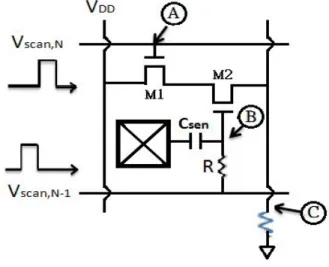
To overcome the above issues, we propose a new concept of using the different delay times of an RC low-pass filter. The proposed sensing circuit is shown in Fig. 1. M1 and M2 are connected in series and controlled by the consecutive scan lines N and N-1, respectively. The TFT M1 is used to select the pixel, and the other TFT M2 is used to sense the touch event. The touch event varies the sensing capacitance Csen, and thus changes the RC time constant. When the pixel is not selected, both M1 and M2 are turned off, and no current is flowing through the TFTs. Just before the pixel is selected, the gate pulse Vscan,N-1 of scan line N-1 is fed to the gate of M2 by way of the RC circuit. At this time, if the pixel is not touched, the sensing capacitor Csen is small and thus the gate pulse is less distorted. In such a case, the gate pulse can go back to OFF earlier than the moment that Vscan,N of scan line N turns on M1.
2
Thus, there is no current passing through M1 and M2. On the other hand, if the pixel is touched, the presentation or increase in Csen makes the gate pulse Vscan,N-1 falling to OFF at a lower rate. By properly designing the resistance R according to the timing of the scan lines and Csen, we can make M2 temporarily ON while M1 is selected. Therefore, a transient current occurs and it can be used as the signal of touch. It is very easy to determine the touch event from the significant output ON current, which makes the read out circuit very simple.
3. Experimental Verification
3.1 Simulation
In this method, the pixel outputs sensing signal in current mode. It is more proper to be applied in a large size panel because the current signal does not affected by the stray capacitance and resistance on the signal bus. The device variation only affects the output current level but not the response time that carries the information of touch. Moreover, this proposal does not consume readout power when sensing pixel is not touched. This can minimize the power consumption of operation. Thus, all the issues mentioned above are avoided.
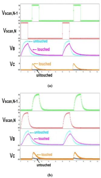
The scan pulse waveform is very concerned in the proposed circuit. The scan pulse can be seriously distorted if the sensing pixel is located at the far-end of scan line. The function of the proposed method should be confirmed for the pixels near the end of scan line. The software HSPICE is used to perform a preliminary simulation for the proposed circuit and verify the advantages mentioned in last paragraph. Fig. 3 shows the simulation results of the pixels sited the near- and far-end of a scan line. The far-end scan pulse is applied with distortion time constant set as 20% of the gate pulse width, which corresponds to the reasonable RC distortion at the end of a row line. The sensing circuit considering the scan delay is set as Fig.2.
In applications, the proposed method accurately determines the touch location by the scanning y and the readout channel x, which supports multiple touch operation like the other active matrix sensors. The proposed circuit can
Fig. 2 The scheme of the proposed touch sensing circuit with the scan and data delay consideration
(a)
(b)
Fig. 3 The simulation results of (a) near (b) end of scan line.
be applied in both external and in-cell types of TSPs. For the external type, the sensing capacitance is formed by the gate electrode of M2 and a floating pad for touch. For in-cell TSPs, we can use liquid crystal capacitance to be Csen, which is varied by the external force to compress the cell gap. It is even better that the pixel circuit only occupies a small aperture because of its simple configuration.
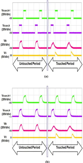
3.2 Measurement
For verification, the proposed circuit is implemented by two discrete IGZO TFTs, one resistor, and one capacitor. Two values of capacitance are used in our experiment. One of the two capacitors is selected to be 2.64 times of the other one to simulate the touched and untouched cases. Two pulses corresponding to scan,N and scan,N-1 are fed to the gate electrodes of the TFTs with and without the RC circuit, respectively. In order to prove the easiness of read out, we simply use a resistor to measure the transient current.
3
capacitance is larger, more obvious RC delay appears, as illustrated in the touched period in Fig. 3. It can be seen that the RC delay in the voltage at node B (VB) keeps M2 TFT turning ON temporarily while M1 is turned ON by the gate pulse of scan,N (VA). Thus, a transient signal is observed as the voltage of the resistor (VC), which reflects the current output from the pixel. On the other hand, for the smaller capacitance, since the pulse of VB goes OFF before VA goes ON, there is no current signal occurs. The results verify the function of the proposed method.
It should be mentioned that this circuit can also be implemented by a-Si:H TFTs as the demonstration shown in Fig.5. The LED and the oscilloscope waveform indicate whether the touch event happens or not.
(a)
(b)
Fig. 4 Measurement result of the proposed circuit
(a)
(b)
Fig. 5 The circuit is demonstrated by a-Si:H TFTs (a) touched (b) untouched.
4. Conclusion
A novel but simple concept of using time-constant change to make the active matrix touch sensor is proposed. The new circuit has many advantages. Firstly, the output signal of the transient ON current is significant and thus can be easily read out by low cost ICs, even for very large area touch panels. Secondly, current signal only occurs when a pixel is touched. The power consumption in operation is greatly reduced. Thirdly, the non-uniformity in the characteristics of TFTs only varies the current level of output signal but not its transient time, as long as the resistances are uniform. Fourthly, the circuit occupies small area and the two required scan pulses are the same as those in AMLCD, which makes this circuit suitable for the in-cell application. The proposed method provides an excellent way of implementing large area active matrix touch panels.
4 References
[1] M. K. Kang, et al., “Advanced Technology Based on a-Si or LTPS TFT for high performance Mobile Display”, SID Symp. Dig., pp. 1262-1265, 2007. [2] C. Brown, et al., “A 2.6 inch VGA LCD with optical
input function using a 1-Transistor Active-Pixel Sensor”, ISSCC, Session 7, pp. 132-133, 2007.
[3] T. Eguchi, et al., “A 1300-dpi optical image sensor using an a-Si:H photo diode array driven by LTPS TFTs”, SID Symp. Dig., pp. 1097-1100, 2007.
[4] H. Hayashi, et al., “Optical Sensor Embedded input display usable under high-ambient light conditions”, SID Symp. Dig., pp. 1105-1108, 2007.
[5] G. J. A. Destura, et al., “Novel Touch Sensitive In-Cell AMLCD”, SID Symp. Dig., pp. 22-23, 2004. [6] B. H. You, et al., “12.1-inch a-Si:H TFT LCD with
Embedded Touch Screen Panel”, SID Symp. Dig., pp.830-833, 2008
[7] C. S. Kim, et al., “Active Matrix Touch Sensor Perceiving Liquid Crystal Capacitance with Amorphous Silicon Thin Film Transistors”, Jpn. J. Appl. Phys., vol. 49, no.3, part 3, 2010
[8] B. H. You, et al., “LCD Embedded Hybrid Touch Screen Panel Based on a-Si:H TFT”, SID Symp. Dig., pp.439-442, 2009.
[9] H. S. Park, et al., ”Touch-Sensitive Active-Matrix Display with Liquid-Crystal Capacitance Detector Arrays”, Jpn. J. Appl. Phys., vol. 49, no.3, part 2, 2010 [10] C.-F. Wu, C.-H. Tsao, C.-W. Wang, Y.-T. Chen, K.-H.
Tsai, Y.-P. Huang,, C.-M. Hung, T.-R. Chang, M.-S. Lai, M.-F., Chiang, B.-Y. Liu, and C.-T. Liu, “Touch Panel Liquid Crystal Displays,” China Patent, publication number CN 1916712A
SID Display Week 2011 出國心得報告
報告人:交大光電系副教授 戴亞翔
一、 參加會議經過
這次所參加的會議為 SID(Society for Information Display,國際資訊顯示 學會年會)所主辦的 2011 年國際顯示科技研討會,於 5 月 17 日~5 月 20 日 在美國洛杉磯舉行,參加此會議對我們從事顯示器相關研究領域的人而 言,除了可以接觸到不同領域中最新的研發成果及未來的研究趨勢,更可 以與世界各地研究顯示器技術的高手進行面對面的交流,獲益甚多。 5/16 晚間抵達西雅圖,規劃要聽取的研究相關的論文報告,註記想要 問作者的問題。
本人為 Session 26: Panel-Driving Technology 之 Co-Chair,於 5/17 上午 7:00 參加 Chair / Co-Chair 會議,聽取主持會議時的注意事項宣導。 本人為 SID Program committee 之 Display Electronics Subcommittee 的
一員,於 5/18 上午 7:00 參加 Program committee 會議,開始籌備 SID 2012 的相關工作,並討論 Display Electronics Subcommittee 的未來規 劃。
5/17-5/20 的 Symposium 期間,共聽取了 Oxide TFTs I,Mobile Display Technology,AMOLED And AMLCD TVs,Panel-Driving Technology , 3D-TV: OLED,Oxide TFTs II,Capacitive Touch System,OLED Displays II,Optical Touch System,…等 Session 的口頭論文發表。
5/19 在會議的 POSTER SESSION 中,由本人指導的博士生周祿盛等 人 發 表 論 文 編 號 P.197 : Active-Matrix Touch Sensor Detecting
Time-Constant Change Implemented by IGZO TFTs;有許多與會者對我
們所發表的論文內容很有興趣,問了許多深入的問題,與我們作了充 分的討論,從他們的回應更確認我們研究方向是正確的。其中 Apple 公司的姚博士,十分肯定此論文的概念,建議我們先不要管成本的問 題,把觸控訊號加強到最大,才會突顯我們的技術能力,cost down 的問題再讓生產的廠商自行去設法即可。
在會議期間抽空參觀會議展覽,與去年相比,來自台灣的廠商更少 了,面板大廠 AUO 或 CMO 等皆未參加,只有元太科技以較大的規 模展示電子紙技術;來自韓國的顯示器大廠 Samsung 和 LG 仍維持與 去年相同的大規模的展出。 二、 與會心得 此次會議的主要目的是報告本實驗室所發表之論文為壁報論文編號 P.197, 擔任 Session 26 的 co-chair,以及參加 Program committee 會議。在此國際性大型 會議進行發表,能和與會的專家學者們進行更深一層的討論,提高台灣及本校在 國際間研究的知名度與能見度,許多參觀者提出了問題,並討論未來可以繼續研 究的方向與在應用上可能的發展,對我將來在進一步的研究極具助益。 在這次的研討會中,有非常多金屬氧化物半導體(oxide semiconductor,OS) 薄膜電晶體(TFTs)的相關論文,本次本人實驗室所發表的論文亦與此有關,可見 OS TFTs 是目前眾所矚目的研發重點,另一方面,在展示會場中已有許多 OS TFT 的產品展出,可見目前技術從實驗到生產所花的時間縮得非常短,顯出目前技術 進步的快速與激烈競爭。
另一個與會心得是,非常多篇論文所涉及的領域,例如,在 AMOLED 的 Session 中聽到的論文,會涉及 OS TFT;而 3D TV 的 Session 中聽到的論文,又
會與 OLED 的快速驅動有關,可見現今的顯示技術的研究,不再只是單一技術, 而是多個領域的整合成果,這是未來從事相關研究要特別注意的。
出席國際學術會議心得報告
計畫編號 99-2221-E-009-121-
計畫名稱
非晶矽薄膜電晶體作為光感測元件及電路之研究(II)
出國人員姓名
服務機關及職
稱
周祿盛/交通大學/博士生
會議時間地點 May 15 - May 20, 2011
會議名稱
Society For Information Display
發表論文題目
Active Matrix Touch Sensor Detecting Time-Constant Change
Implemented by IGZO TFTs
一、
參加會議經過
5 月 7 日由台灣出發,到會議所在地洛杉磯為當地 7 日下午三點半鐘,而
後一星期參訪由 SID 大會所推薦的當地景點。16 日於會議舉行地 Los Angeles
Convention Center 註冊後,在往後三天聽取了 Oxide TFT1、Oxide TFT2、
Panel-driving Technology、Capacitive Touch System、Touch System 等 Oral
Section,並將其成果整理攜回台灣與團隊中夥伴一起分享。
會議中於空檔時間參觀展示區,瞭解各家廠商在今年度的技術重點及突
破。本次投稿至 SID 的成果被安排於 Touch System 中,並在 19 號下午 poster
展示期間與與會人士進行交流,為其介紹本團隊之研究成果,頗獲好評。最後,
於 20 日凌晨 1 時 35 分搭機回國。
二、
與會心得
本次會議除了展示本身研究成果外,聽取與自身有關之研究也是此行之
重點,因此有關 Oxide TFT 及觸控應用之 section 都盡量前往聆聽。對於自己
研究上問題,如微小訊號讀取之問題,與 Oral Speaker 有充分之溝通與幫助,
相信對研究上必有很大助益。
而另外一個大收穫是在展場上,除了各家大廠令人驚艷的最新技術外,
還可以從展場中了解現在業界專注研究的方面及未來的趨勢為何。很顯然的3D
技術絕對會是近幾年市場上最受矚目的項目之ㄧ,相較於去年SID各家廠商的展
出,今年的產品更趨成熟與實用。而支援多點觸控技術更已進展到可同時偵測
超過20個觸控點,不同的觸控技術也在會議Oral與Poster Section中被發表,
包括本團隊所提出之" Active Matrix Touch Sensor Detecting Time-Constant
Change Implemented by IGZO TFTs"。此外,在綠色能源的議題下,低功耗高畫
質之顯示器亦不斷被研究改進中。
三.結語
本次參與SID會議攜帶回論文集光碟一份,將提供台灣沒有參與的實驗室夥
伴有機會閱讀國外研究的論文,還有展覽會場拍攝的一些展示照片也提供台灣
的夥伴有機會了解業界的動向與發展,能夠有這樣的機會到國外參加會議是一
次很好的歷練,很感謝國科會給予的補助,相信此經費也可助於日後的相關研
究與發展。
國科會補助計畫衍生研發成果推廣資料表
日期:2011/10/26國科會補助計畫
計畫名稱: 非晶矽薄膜電晶體作為光感測元件及電路之研究(II) 計畫主持人: 戴亞翔 計畫編號: 99-2221-E-009-121- 學門領域: 光電子材料元件與模組無研發成果推廣資料
99 年度專題研究計畫研究成果彙整表
計畫主持人:戴亞翔 計畫編號: 99-2221-E-009-121-計畫名稱:非晶矽薄膜電晶體作為光感測元件及電路之研究(II) 量化 成果項目 實際已達成 數(被接受 或已發表) 預期總達成 數(含實際已 達成數) 本計畫實 際貢獻百 分比 單位 備 註 ( 質 化 說 明:如 數 個 計 畫 共 同 成 果、成 果 列 為 該 期 刊 之 封 面 故 事 ... 等) 期刊論文 2 2 100% 研究報告/技術報告 0 0 0% 研討會論文 0 0 0% 篇 論文著作 專書 0 0 0% 申請中件數 0 0 0% 專利 已獲得件數 0 0 0% 件 件數 0 0 0% 件 技術移轉 權利金 0 0 0% 千元 碩士生 3 3 100% 博士生 1 1 100% 博士後研究員 0 0 0% 國內 參與計畫人力 (本國籍) 專任助理 0 0 0% 人次 期刊論文 0 0 0% 研究報告/技術報告 0 0 0% 研討會論文 0 0 0% 篇 論文著作 專書 0 0 0% 章/本 申請中件數 0 0 0% 專利 已獲得件數 0 0 0% 件 件數 0 0 0% 件 技術移轉 權利金 0 0 0% 千元 碩士生 0 0 0% 博士生 0 0 0% 博士後研究員 0 0 0% 國外 參與計畫人力 (外國籍) 專任助理 0 0 0% 人次其他成果