國 立 交 通 大 學
電子工程學系電子研究所
博 士 論 文
高電壓橫向擴散金氧半電晶體中
暫態熱載子效應與元件模型之探討
Investigation of Transient Hot Carrier Stress and
Device Modeling Issues in High-Voltage Lateral Diffused
Metal-Oxide-Semiconductor Field Effect Transistors
研 究 生 :鄭志昌
高電壓橫向擴散金氧半電晶體中
暫態熱載子效應與元件模型之探討
Investigation of Transient Hot Carrier Stress and
Device Modeling Issues in High-Voltage Lateral Diffused
Metal-Oxide-Semiconductor Field Effect Transistors
研 究 生:鄭志昌
Student:Chih-Chang Cheng
指導教授:汪大暉 博士
Advisor:Dr. Tahui Wang
國 立 交 通 大 學
電 子 工 程 學 系
電 子 研 究 所
博 士 論 文
A Dissertation
Submitted to Department of Electronics Engineering and Institute of Electronics
College of Electrical and Computer Engineering National Chiao Tung University
in Partial Fulfillment of the Requirements for the Degree of Doctor of Philosophy
in
Electronics Engineering May 2009
Hsinchu, Taiwan, Republic of China
高電壓橫向擴散金氧半電晶體中暫態熱載子效應與元件模型之探討
研究生: 鄭志昌
指導教授: 汪大暉博士
國立交通大學
電子工程學系
電子研究所
摘要
隨著電源管理日趨重要,橫向擴散金氧半導體場效電晶體(LDMOS)於高電 壓整合型電路中的使用也日趨廣泛。在高功率的操作下,熱載子引發的可靠性問 題及元件模型的建立仍然是最大挑戰。 本篇論文將針對 LDMOS 的可靠度與元件模型的建立做一系列探討。首先, 吾人提出一個具有特殊接觸電極的 LDMOS 結構,藉以量測 LDMOS 中通道 (channel)部分的內部電壓(internal voltage)、電流、與低頻雜訊。兩個利用此種特 殊結構的例子將在第二章中被討論;一個是對自我加熱效應(self-heating effect) 的研究,另一個是對通道電流與 LDMOS 電流的特性分析。在自我加熱效應的研 究中,吾人提出一個以內部電壓為觀察指標的研究方式,觀察到自我加熱效應所在第三章中,針對熱載子效應所導致的氧化層傷害,吾人提出一個新式三段 式電荷幫浦(three-region charge pumping)的量測方法加以研究。利用此方法,我 得以確認不同傷害模式下的氧化層損傷位置,並可以進一步知道所產生的損傷缺 陷特性。我們的研究結果顯示,在最大閘極電流(max. IG stress)模式下,將導致 最大的汲極電流與次臨限區斜率(subthreshold slope)的退化,退化的原因為通道 區的表面缺陷(interface trap)產生與鳥嘴區(bird’s beak region)的負電荷量(negative oxide charge)累積,其產生的速度將可從三段式電荷量測幫浦中個別萃取。同時, 我們也將利用二維元件模擬與低頻雜訊量測方法進一步確認實驗結果。
經由前面章節的了解,在第四章中,吾人將利用特殊結構研究自我加熱效應 所引發的暫態熱載子效應(transient hot carrier effect)。同時,利用二維元件模擬驗 證實驗結果,並用來分析交流頻率與元件退化間的關聯性。吾人研究結果發現, 熱載子效應在交流偏壓下的電流退化,將比直流偏壓下的電流變化更為嚴重,其 原因在於自我加熱效應的消失將造成熱載子的增加。
最後,吾人發展出一個雙組合元件模型(a two-component device model),用 來描述 LDMOS 的電流特性,並將模擬自我加熱效應所引發的內部電壓改變。此 LDMOS 模型將使用一種新的模型建立方法,以低閘極/高閘極電流分別建立通道 區與淡摻雜區(drift region)的模型。並利用內部電壓控制有/無自我加熱效應下的 汲極電流。經由比較後發現,我們的模型在所有的操作電壓下均可以準確的預測 汲極電流,這範圍包含次臨限區(subthreshold)到臨限區以上(super-threshold)、有 自我加熱情形及無自我加熱情形都可準確描述。
Investigation of Transient Hot Carrier Stress and Device Modeling Issues
in High-Voltage Lateral Diffused Metal-Oxide-Semiconductor
Field Effect Transistors
Student: Chih-Chang Cheng
Advisor: Dr. Tahui Wang
Department of Electronics Engineering & Institute of Electronics
National Chiao-Tung University
Abstract
Lateral diffused MOS (LDMOS) are extensively used in today’s high-voltage integrated circuits, particularly where power handling is important. Hot carrier induced reliability concerns and device modeling problems in such high power operation are being aroused.
The objective of this dissertation is to investigate both reliability and device modeling issues in LDMOS transistors. First of all, a novel LDMOS structure incorporating an additional metal contact in the drift region is fabricated, which allows us to probe internal voltages, currents, and flicker noise in the channel-part of a
measured. Our study shows that the internal voltage method is more sensitive to self-heating than a conventional drain current method in a LDMOS. In the other example, the metal contact structure is used to investigate the channel and the LDMOS characteristics. Current and flicker noise in the channel and in the LDMOS are measured. Our experiments show that both drain current and drain flicker noise at low-VGregime are major determined by the channel-part of a LDMOS, which imply a new extraction method for device modeling and a characterization technique for hot carrier effects.
In Chapter 3, hot carrier stress induced oxide degradation in n-LDMOS is investigated by using a novel three-region charge pumping technique. This technique allows us to locate oxide damage area in various stress modes and gain insight into trap creation properties. Our characterization shows that a max. IG stress causes a largest drain current and subthreshold slope degradation because of both interface trap (Nit) generation in the channel region and negative bulk oxide charge (Qox) creation in thebird’sbeak region.Thedensity ofNitand Qoxcan be separately extracted from the proposed charge pumping method. A numerical device simulation and drain flicker noise are performed to confirm our result.
Based on the understanding of Chapter 3, self-heating induced transient hot carrier effects are investigated in Chapter 4 by using the metal-contact structure introduced in Chapter 2. The AC stress-frequency dependence of device degradation is characterized and evaluated by a two-dimensional numerical simulation. Our result shows that drain current degradation in AC stress is more serious than in DC stress because of the reduction of self-heating effect.
Finally, a two-component device model including self-heating induced internal voltage transient in a LDMOS is developed. A new modeling method for the channel/drift regions is proposed by fitting a low-VG/high-VG drain current. Our
modeling method uses an internal voltage to control drain current in self-heating and in non-self-heating conditions. A comparison with dc measurements shows that our model provides an accurate description in all regimes of operation, ranging from subthreshold to super-threshold, for both self-heating and non-self-heating conditions.
致謝
首先,這本博士論文的完成,必須歸功於我的指導老師汪大暉教
授。汪教授對於研究的熱誠與敏銳度讓我深深佩服;其深厚的學術基
礎與嚴謹的研究態度,深化我對於許多事情的看法,並改變我對於人
生的態度,對我的人生觀影響極為深遠。
在論文的研究方面,必須感謝過去許多曾經指導過我的學長姐
們,及一起參與研究的同學及學弟妹們。首先感謝蔡慶威、陳旻政、
吳俊威、古紹泓、詹前泰學長在我研究過程中的指導與鼓勵;感謝江
欣凱、邱凱翎、李兆琪學長姐在我剛進研究生活的協助與討論。同時,
我也感謝游建文、王銘德同學在研究路程的協助,及邵晉輝、杜冠潔、
林家福、熊勖廷、周佑亮學弟妹在實驗執行上的大力幫助,以及馬煥
淇、唐俊榮、許智維、郭晉豪、李冠成、薛至宸、李智雄、李致維、
吳致融、許家源、林彥君、趙元鵬、邱子華、邱榮標、杜文仙學弟妹
協助前瞻元件與技術實驗室的運作,並帶給實驗室許多歡笑與趣味。
另外,感謝台積電謝定華副處長,提供我研究上相關的協助及意見。
再者,也感謝國家奈米實驗室黃國威博士在實驗儀器上的協助。最
後,感謝我的大學好友楊玉麟、陳季汎陪我度過漫長的博士班生涯。
其次,感謝我的父親、大姐、二姐、三姐、以及陪伴我 10 年剛
於 4 月 19 日結婚的老婆黃郁惠,在我漫長的求學期間給我的鼓勵與
支持,有你們在背後無怨無悔的付出與關心,讓我毫無顧忌的專注於
論文研究,使得這本博士論文得以順利完成。
在此,謹將這份榮耀獻給為家庭付出許多的父親,指導我的汪大
暉教授,及將攜手一輩子的老婆郁惠。
Contents
Chinese Abstract i
English Abstract iii
Acknowledgement vi
Contents vii
Figure Captions x
Table Captions xvi
List of Symbols xvii
Chapter 1 Introduction 1
1.1 Backgrounds 1
1.2 Organization of the Dissertation 3
Chapter 2 A Novel Metal Contact Structure for Self-Heating Effect and Device Characterization
8
2.1 Introduction 8
2.2 An Internal Voltage Method to Characterize Self-Heating
9
2.2.1 Internal Voltage Transient 10 2.2.2 Comparison of VIMethod and Conventional
IDMethod
Chapter 3 Physics and Characterization of Various Hot-Carrier Degradation Modes in LDMOS by Using a Three-Region Charge-Pumping Technique
25
3.1 Introduction 25
3.2 Three-region Charge Pumping Measurement 27 3.3 Flicker Noise Measurement 28 3.4 Various DC Hot Carrier Stress Modes 29 3.3.1 Maximum IBStress Mode 29 3.3.2 VG∼(1/2) VDStress Mode 30 3.3.3 Maximum IGStress Mode 31
3.5 Summary 32
Chapter 4 Impact of Self-Heating Effect on Hot Carrier Degradation in High-Voltage LDMOS
55
4.1 Introduction 55
4.2 Self-Heating Characterization 56 4.3 Degradation Characteristics in AC/DC Stress 57
4.4 Summary 58
Chapter 5 A Two-Component LDMOS Model including Self-Heating Effect
74
5.1 Introduction 74
5.2 Model Description 75
5.3 A New Modeling Method 76
5.3.2 VIController Model 77
5.3.3 Self-Heating Model 78
5.4 Results and Discussions 78
5.5 Summary 79
Chapter 6 Conclusion and Future Work 94
6.1 Conclusion 94
6.2 Future Work 95
Appendix A List of MOS Parameters 97
Appendix B SPICE Model Implementation Example 101
Appendix C Derivation of VIsat 104
References 105
Vita 114
Figure Captions
Chapter 1Fig. 1.1 Applications of power devices in relation to their voltage and current ratings, from [1.1].
Fig. 1.2 Applications of power semiconductor devices provided as a function of system operating frequency and power handling capability, from [1.1]. Fig. 1.3 The organization of the dissertation.
Chapter 2
Fig. 2.1 Top view of a novel metal contact structure. Three different regions are indicated by Lch (channel region), Lacc (accumulation region), and LFOX (field-oxide region). A contact (VI) is placed in the accumulation region. Fig. 2.2 Cross-section of the metal contact structure to characterize self-heating
effect. The cross-section is plotted from the line (A-A’)in Fig.2.1. The metal contact (VI)isarranged in thebird’sbeak region with an n+implant. Fig. 2.3 Measured internal voltage (VI) transient due to self-heating. VDis 40V. The
gate voltage is switched from 15V to 40V at t=0s. Two-stage transient is noticed.
Fig. 2.4 Simulated temperature distribution along the device at VD=40V and VG=40V.
Fig. 2.5 (a) Internal voltage versus drain voltage with and without self-heating effect. The full squares (w/ SHE) are obtained by Agilent 4156 while the open squares (w/o SHE) are obtained from the measurement setup in Fig. 2.2. (b) Drain current versus drain voltage measured by Agilent 4156 (full squares) and by an external resistor method (open squares).
Fig. 2.6 Drain current versus internal voltage in a LDMOS. The reduction of VIand
5 6 15 16 7 17 18 19 20
IDdue to self-heating is denoted byVIandID, respectively.
Fig. 2.7 ID-VD in LDMOS and in the proposed new structure. (a) At lower VG (VG<10V). (b) At higher VG(VG>10V).
Fig. 2.8 I-V Measurement setup for device characterization. The VIis measured by forcing a zero current in SMU 3. VG/VDare given by Agilent 4156.
Fig. 2.9 Comparison of metal-contact structure (ID-VD) characteristics and channel part of metal-contact structure (ID-VI) characteristics. (a) At lower VG. (b) At higher VG.
Fig. 2.10 Noise power spectrum density versus current flow in LDMOS, channel part of the LDMOS, and drift-region part of the LDMOS. (a) VG=2V, (b) VG=9V, and (c) VG=18V.
Chapter 3
Fig. 3.1 (a) Cross-section of a n-LDMOS and flat-band (solid line) and threshold (dash line) voltage distributions. The device is divided into three parts, i.e., 1) Lchan (channel region), 2) Lacc (accumulation region), and 3) Lfox (field oxide region). (b) Illustration of a charge pumping measurement waveform. Vgh=12V is fixed and Vglvaries from +3.6V to -40V.
Fig. 3.2 Typical CP current in a n-LDMOS. The three stages of the CP current correspond to the three regions of the device. The flat-band voltage of each
21 23 24 22 34 35
IB), B (VG~1/2VD), and C (maximum IG) are indicated.
Fig. 3.5 (a) Charge pumping current versus Vgl before and after 1400 sec. mode A stress. (b) Two-dimensional device simulation of impact ionization generation (IIG) distribution in stress mode A.
Fig. 3.6 Comparison of normalized low flicker noise before and after mode A stress. (a) At a lower VG(VG=2V) and (b) at a higher VG(VG=18V).
Fig. 3.7 (a) Charge pumping current versus Vgl before and after 1400 sec. mode B stress. The shift of the flat-band voltage in stage 2 implies the generation of negative oxide charge in the accumulation region. (b) Two-dimensional device simulation of impact ionization generation (IIG) in stress mode B. Fig. 3.8 The charge pumping results in stress mode B for different stress times. Fig. 3.9 Region (II) oxide-trapped charge growth rate in stress mode B.
Fig. 3.10 Linear drain current degradation (Idlin) rate measured at VG/VD=40V/0.1V in stress mode B.
Fig. 3.11 Comparison of normalized low flicker noise before and after mode B stress. (a) At a lower VG(VG=2V) and (b) at a higher VG(VG=18V). The increase of (Sid/Id2) at a higher VG is attributed to the creation of negative oxide charge in the accumulation region.
Fig. 3.12 (a) Charge pumping current before and after 1000 sec. mode C stress. Upward shift in stage 1 Icp indicates interface trap generation in the channel and rightward shift in stage 2 Icp implies oxide charge creation in the
38 39 40 41 42 43 44 45
accumulation region. (b) Two-dimensional device simulation of impact ionization generation (IIG) distribution in stress mode C. Two IIG regions are found; One is in the channel region and the other is in the accumulation region.
Fig. 3.13 Comparison of normalized flicker noise before and after mode C stress. (a) At a lower VG(VG=2V) and (b) at a higher VG(VG=18V). The increase of (Sid/Id2) at a lower VG and at a higher VG are attributed to the creation of Nitin the channel and Qoxin the drift region, respectively.
Fig. 3.14 Subthreshold characteristics before and after mode C stress. The swing degradation is attributed to interface trap generation in the channel region. Fig. 3.15 The linear drain current versus VGbefore and after mode C stress.
Fig. 3.16 Simulated drain current versus gate voltage without and with oxide charges. (a) The oxide charge is placed in the channel and (b) the oxide charge is placed in the bird’s beak region.
Fig. 3.17 Region (I) interface trap growth rate in stress mode C. Fig. 3.18 Region (II) oxide charge growth rate in stress mode C.
Fig. 3.19 Idlin degradation versus stress time in stress mode C. The degradation is
46 47 48 49 50 51 52
Chapter 4
Fig. 4.1 Fast transient measurement setup for drain current and internal voltage (VI) characterization. The resistance (10is small than the total resistance (~40V/10mA ~4k). A gate pulse and constant VDare used.
Fig. 4.2 (a) Normalized drain current (ID/W) versus drain voltage in small and large gate width devices in DC measurement (Agilent 4156). (b) The ID/W from a DC and a fast transient measurement for the large width device.
Fig. 4.3 Internal voltage versus gate voltage measured by Agilent 4156 and by a transient measurement setup.
Fig. 4.4 Substrate current and gate current versus gate voltage in a LDMOS. Two hot carrier stress modes are shown, maximum IB stress and maximum IG stress.
Fig. 4.5 Linear drain current degradation (VG/VD= 40V/0.1V) in two hot carrier stress modes. DC and AC stresses have the same cumulative stress time. AC stress has a frequency of 20kHz and a duty cycle of 10%.
Fig. 4.6 (a) Idlin degradation versus stress frequency with a duty cycle of 10%. A corner frequency ( f1 ) is around 20kHz. (b) Idlin degradation versus duty cycle for a frequency of 20 kHZ.
Fig. 4.7 Idlindegradation versus pulse duration (=duty cycle/frequency) in AC stress. The corner time is around 5s.
Fig. 4.8 The internal voltage (VI) transient in a pulsed gate and DC drain voltage
60 61 62 63 64 65 66 67
(VD=40V) condition. The waveforms of VI and VG are plotted. The onset time for SHE is ~5s.
Fig. 4.9 Three-region charge pumping measurement results after maximum IG AC and DC stress. A VgLshift is in the accumulation region and a Icpincrease is in the channel region.
Fig. 4.10 Substrate current and gate current versus gate voltage for different temperatures.
Fig. 4.11 Simulation of a temperature distribution with SHE. The ambient temperature is 300K. X axis is the direction from source to drain. Y axis represents the depth. (a) VG/VD=10V/40V. (b) VG/VD=40V/40V.
Fig. 4.12 Internal voltage change (VI(non-SHE)-VI(SHE)) versus gate voltage from measurement and from simulation.
Fig. 4.13 Two-dimensional device simulation of impact ionization generation (IIG) rate at VG/VD=40V/40V. (a) SHE is included and (b) SHE is not included. Fig. 4.14 Idlindegradation rate after AC and DC stress in maximum IGstress condition.
The AC stress frequency is 20 kHz and the duty cycle is 10%.
68 69 70 71 72 73
Illustration of different operating regions controlled by each component. Fig. 5.2 Illustration of input/output process of the LDMOS model. The VI is
controlled by VGand VD. The IDis determined by VIand VG.
Fig. 5.3 Illustration of the VI controller. An internal voltage transient due to self-heating (SH) is taken into account. The VI at t=0+ is expressed as a function of VGand VD(listed in Equation 1). TheVItransient is described by a RC network in Fig. 5.9.
Fig. 5.4 A new modeling method for the MOS element and the VI controller. Five extraction steps are indicated, including (1, 2) MOS model, (3) VI simulation step, (4) VIcontroller model, and (5) LDMOS macro-model. Fig. 5.5 A VIsimulation method in step 3. Each measured IDcan extract a simulated
VI. Typical VI simulation is shown in the inset under self-heating (w. SH) and non-self-heating (w/o SH) conditions. The MOS model is obtained from step 1 and 2. This method is performed by a HSPICE simulator.
Fig. 5.6 A comparison of a fitting result during the extraction step of the MOS model. The ID-VGis measured from a LDMOS. The Ich-VGis obtained from the MOS model performed by a HSPICE simulator.
Fig. 5.7 A comparison of fitting results during the extraction step of the MOS model. (a) At lower VG. (b) At higher VG. The ID-VDis measured from a LDMOS. The Ich-VIis obtained from the MOS model. A match between LDMOS and MOS model means no voltage drop in the drift region and thus VI=VD. A
81 82 83 84 85 86
mismatch at VG=40V indicates a voltage drop in the drift region and thus VI is much smaller than VDas current flow is the same.
Fig. 5.8 A comparison of VIcontroller model in a non-SH condition. Symbol is the VI obtained from the VI simulation method. Line represents a simulation result of the VIcontroller model. (a) VI-VD. (b) VI-VG.
Fig. 5.9 A RC network to describe self-heating induced internal voltage transient (VI(t)). Three components are used, including a current source, a resistor R, and a capacitor C.
Fig. 5.10 ID transient and a corresponding VI simulation performed by the VI simulation method. indicates a difference of VI transient due to self-heating.Crepresents a time constant of VItransient.
Fig. 5.11 A comparison of VI transient at VG/VD=40V/40V. Line represents the VI obtained from the VI simulation method. Dash represents the VIobtained from the VIcontroller model. A fitting result ofVI(t) is also indicated. Fig. 5.12 A comparison of IDtransient between measurement and our macro-model. Fig. 5.13 A comparison of ID-VDbetween measurement and our macro-model. (a) At
lower VG. (b) At higher VG. The ID in SH and non-SH conditions are
87 88 89 90 91 92
Table Captions
Chapter 3Table 3.1 Summary of major oxide and device performance degradations in various stress modes.
List of Symbols
C Capacitance f Frequency Gm Trans-conductance IG Gate current IB Substrate current ID Drain current Ich Channel current Icp Charge-pumping current Lch Channel lengthLacc Accumulation region length Lfox Field oxide region length
Nit Interface trap Qox Bulk oxide charge q Electronic charge
R Resistor
SId Drain current noise power spectrum density on Onset time of a self-heating effect
s Saturation time of a self-heating effect C Corner time constant of self-heating effect VG Gate voltage
VD Drain voltage
Vgh High-level voltage of voltage waveform Vgl Low-level voltage of voltage waveform VFB Flat-band voltage
VI Internal voltage of LDMOS VI,eff Effective internal voltage VTH Threshold voltage
W Channel width
Chapter 1
Introduction
1.1 Backgrounds
The increasing applications of high-voltage integrated circuits force the continuous evolution of modern power semiconductor devices. The first applications of power integrated circuits, about 40 years ago, were in voltage regulators and audio amplifiers [1.1]. A monolithic integrated circuit that combines power and signal circuitry on a chip is developed to reduce electronic products size, weight, and cost. Nowadays, power devices are presented in various applications. Fig. 1.1 shows applications for power semiconductor, where the boxes indicate the device voltage and current ratings required from system [1.2]. The power devices at relatively lower voltages (<100V) and current levels (<10A) are usually integrated with control circuits [1.3]. At higher power levels, such as in traction and high voltage DC transmission systems, the systems are implemented using discrete components [1.3].
From operating frequency point of view, power thyristors, bipolar power transistors, and power MOSFET play different roles in the development of power devices. A comparison of operating frequency for different applications is illustrated in Fig. 1.2. The power devices used in the applications are indicated in the figure. Power thyristors are designed for blocking voltage above 6000V and have relatively slow switching speed [1.3]. These devices are suitable for systems with low operating frequency. Two examples of such applications are high voltage direct current (HVDC) power transmission networks and high power motor drives used in steel mills [1.2]. For relatively lower blocking voltage and higher operating frequency, bipolar power transistors become more attractive. The blocking voltage of these devices has been
extended to 500V ~ 1200V with operating frequency of ~50kHz [1.3]. As system operating frequency is much higher, power MOSFET transistor provides a better solution and simplicity control. These devices are operated at frequency above 100 kHz and the blocking voltages are less than 200V [1.4].
In addition, an integrated bipolar, CMOS, and power DMOS (BCD) technology has been developed in the mid eighties. This technology allows the integration of a wide variety of high-voltage device structures [1.5]. Among the candidates of high-voltage devices, lateral diffused MOS (LDMOS) transistors are attractive because the advantage of process compatible to CMOS technology. The LDMOS has been widely used in today’shigh-voltage and high-current output circuits [1.6], from a standard 12-V automotive battery [1.7] to 100-V plasma display panel drivers [1.8].
Several issues in LDMOS transistors are presented, including (a) hot carrier degradation induced reliability constraint [1.9] [1.6], (b) high power induced temperature rising or self-heating effect [1.10] [1.11], and (c) device modeling [1.12]. Since an LDMOS processes an intrinsic channel region and a lightly doped drift region, its hot carrier degradation mechanisms are different from a traditional MOSFET. The lightly-doped drift region was reported to be the major limitation for hot carrier degradation because of a specific double-hump substrate current behavior [1.9]. Besides, an increasing voltage/current in a LDMOS tends to raise device operating temperature and result in self-heating effect (SHE). Anghel et al. found that
temperature distribution in a LDMOS [1.14]. Larger voltage drop across the lightly-doped drift region causes a higher temperature rising in this area [1.15]. A temperature difference between the channel and drift regions leads to an internal voltage change in a LDMOS [1.15]. This SHE induced internal voltage change, however, cannot be described by a conventional SHE model [1.10] [1.16]. Thus, a new SHE model, which considers both the non-uniform temperature distribution and SHE induced internal voltage change, is necessary.
1.2 Organization of the Dissertation
The organization of this dissertation is schematically illustrated in Fig. 1.3. A novel LDMOS structure incorporating a metal contactin thebird’sbeak region is fabricated and will be described in detail in Chapter 2. With the use of the metal contact structure, internal voltages during the device operation are retrieved. A comparison of I-V characteristics between LDMOS and channel-part of LDMOS is discussed in Chapter 2. In addition, an internal voltage transient due to self-heating effect is also investigated in Chapter 2 and modeled in Chapter 5.
In Chapter 3, degradation of lateral diffused MOS transistors in various DC hot-carrier stress modes is investigated. A novel three-region charge-pumping technique is proposed to characterize interface trap (Nit) and bulk oxide charge (Qox) creation in the channel and in the drift regions separately. The growth rates of Nitand Qox are extracted from the proposed method. A two-dimensional numerical device simulation is performed to gain insight into device degradation characteristics in different stress conditions. The impact of oxide trap property and location on device electrical characteristics is analyzed from measurement and simulation.
In Chapter 4, self-heating induced transient hot carrier effects in high-voltage n-LDMOS are investigated. A novel LDMOS structure incorporating a metal contact
in thebird’sbeakregion is utilized, which allows us to probe an internal voltage transient in hot carrier stress. The AC stress-frequency dependence of device degradation is characterized and evaluated by a two-dimensional numerical simulation.
In Chapter 5, an internal-voltage-based LDMOS SPICE model including self-heating effect is proposed. Our model combines a low-voltage MOS element with a high-voltage controller. The MOS parameters are extracted from the LDMOS I-V data in the low-VGregion and in the linear portion of the high-VGregion. A new SHE model, describing an internal-voltage transient rather than a temperature rise, is developed. Modeling results of self-heating and non-self-heating drain currents at various VGand VDare also compared.
Fig.1.1 Applications of power devices in relation to their voltage and current ratings, from [1.1].
D
ev
ic
e
C
u
r
re
n
t
R
a
ti
n
g
(A
m
p
e
re
s)
Device Blocking Voltage Rating (volts)
10
100
1000
10000
0.01
0.1
1
10
100
1000
P o w e r S u p p li e s A u to m o ti v e E le c tr o n ic s F a c to ry A u to m a t. Display Drivers Telecom. Circuits Lamp Ballasts Motor Control Traction HVDCD
ev
ic
e
C
u
r
re
n
t
R
a
ti
n
g
(A
m
p
e
re
s)
Device Blocking Voltage Rating (volts)
10
100
1000
10000
0.01
0.1
1
10
100
1000
P o w e r S u p p li e s A u to m o ti v e E le c tr o n ic s F a c to ry A u to m a t. Display Drivers Telecom. Circuits Lamp Ballasts Motor Control Traction HVDCFig. 1.2 Applications of power semiconductor devices provided as a function of system operating frequency and power handling capability, from [1.1].
HIGH VOLTAGE DC TRANSACTION MOTOR DRIVE/TRACTION
UNINTERRUPTIBLE POWER SUPPLY TRANSPORTATION INDUCTION HEATING AUDIO AMPLIFIER TV SWEEP COMMUNICATIONS FLUORESCENT LAMP MICROWAVE OVEN
S
Y
S
T
E
M
P
O
W
E
R
R
A
T
IN
G
(V
O
L
T
-A
M
P
E
R
E
S
)
101 102 103 104 105 106 107 108 109 100 102 103 104 105 106 107 108 101DEVICE OPERATING FREQUENCY (Hz)
HIGH VOLTAGE DC TRANSACTION MOTOR DRIVE/TRACTION
UNINTERRUPTIBLE POWER SUPPLY TRANSPORTATION INDUCTION HEATING AUDIO AMPLIFIER TV SWEEP COMMUNICATIONS FLUORESCENT LAMP MICROWAVE OVEN
S
Y
S
T
E
M
P
O
W
E
R
R
A
T
IN
G
(V
O
L
T
-A
M
P
E
R
E
S
)
101 102 103 104 105 106 107 108 109 100 102 103 104 105 106 107 108 101 100 102 103 104 105 106 107 108 101Fig. 1.3 The organization of this dissertation.
Ch. 2
Metal Contact Structure
Ch. 3
DC hot carrier stress
Reliability
Self-heating effect
w/o SHE Model
Device Modeling
w. SHE model
Ch. 5
Internal-voltage
Ch. 4
AC hot carrier stress
Ch. 2
Metal Contact Structure
Ch. 3
DC hot carrier stress
Reliability
Self-heating effect
w/o SHE Model
Device Modeling
w. SHE model
Ch. 5
Internal-voltage
Ch. 4
Chapter 2
A Novel Metal-Contact Structure
for Self-Heating Effect and Device Characterization
2.1 Introduction
Integration of logic and power devices on the same chip has attracted much attention in recent years [2.1] [2.2]. Many applications, such as power management and RF-applications, require a high voltage/high current operation in the power devices. Among the candidates of high-voltage devices, lateral diffused MOS (LDMOS) transistors are attractive because they can be easily integrated with standard low-voltage CMOS process. A lightly doped area with the use of RESURF (reduced surface field) principle [2.3] is generally adopted in the LDMOS, which can support a high drain-to-source breakdown voltage [2.4] and reduce the device dimension. However, continuous increase in power density with the lightly doped area scaling is now seriously challenged in the progression of CMOS and LDMOS technology [2.5] [2.6]. As power consumption increases, hot carrier degradation [2.7] and self-heating effect [2.8] become two most formidable limitations in the LDMOS. The enhanced self-heating effect may cause a snapback breakdown and result in a thermal runaway in the LDMOS [2.5]. In addition, Roux [2.9] reported that
was processed in a 0.18m CMOS technology with a gate oxide thickness of 100nm and a field-oxide thickness of 500nm. A small metal contact (VI), as compared to the device width, is placed in the drift region. Parts of the N-Well and field-oxide regions are controlled by the poly-gate because of the use of RESURF (reduced surface field) principle [2.3]. An internal voltage change in a normal LDMOS operation will be measured from the VI. Since the complexity of the LDMOS behavior is mostly occurred in the lightly doped drift region, the fabrication of the VI allows us to distinguish the I-V characteristics in the channel and drift regions. In this way, the channel region can be regarded as an intrinsic MOS and the drift region can be considered as a resistance. Thus, the physical effects that take place in the LDMOS can be easily understood and explained in the studies.
2.2 An Internal Voltage Method To Characterize Self-Heating
Self-heating effect (SHE) has been observed in laterally diffused metal-oxide-semiconductor (LDMOS) transistors [2.10] [2.11], particularly when the device is operated in high-voltage/high-current circuits. This effect results in an increase of device local temperature and thus a reduction of the drain current. To characterize SHE, a conventional drain current (ID) method [2.11] [2.12] [2.13] [2.14] is usually adopted. In an IDmethod, a short voltage pulse is applied to the gate and the drain current transient resulting from self-heating is extracted from a voltage drop across an external resistor [2.11] [2.13] [2.14]. In the IDmeasurement, the bias at the drain must be continually adjusted to compensate for the voltage drop across the external resistor [2.15], added to determine the drain current. The adjustment of the drain voltage, however, may lead to an ambiguous thermal time constant and result in a questionable SHE study and SPICE modeling. In addition, the drain current in the saturation region is rather insensitive to the change of a local temperature, which
makes an accurate self-heating measurement more difficult in a LDMOS. Here, we propose a more effective characterization method for SHE.
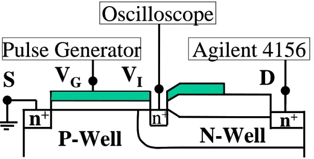
In our method, we measure a self-heating induced internal voltage (VI) change rather than a drain current change. In this way, a series external resistor at the drain is not necessary. To the purpose, we fabricated a special LDMOS device. Fig. 2.2 shows the cross-section of the LDMOS structure, which incorporates a metal contact in the bird’s beak region, thus allowing us to probe an internal voltage directly. The contact area is sufficiently small that the device electrical characteristics are not affected. The device used in this work was processed with a gate width of 20m and a channel length of 3m. The operational voltages are VG=40V and VD=40V.
2.2.1 Internal Voltage Transient
The measurement result of an internal voltage transient due to self-heating is shown in Fig. 2.3. A gate voltage pulse with a low-level voltage of 15V and a high-level voltage of 40V is applied. The low-level voltage of 15V is chosen to prevent VI contact breakdown. The VI transient exhibits two stages in Fig. 2.3. Two time-constants, onand s, are noted. In the initial stage (t<on), VI remains nearly unchanged and on (=~7s) represents an onset time of a self-heating effect. In the second stage (t>on), VIdecreases with pulse time until a dynamic balance between heat generation and dissipation is reached. The saturation time of SHE is denoted by
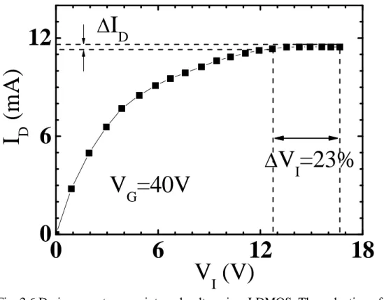
obtained because of a larger voltage drop in the drift region and thus higher power consumption. As a result, the decrease of VI can be realized due to larger mobility degradation in the drift region. A decrease of VI from 16.5V to 13V due to self-heating effect is observed.
2.2.2 Comparison of VIMethod and Conventional IDMethod
For comparison, self-heating induced VIreduction and IDreduction are shown in Fig. 2.5 (a) and (b), respectively. The open squares represent the result without SHE while the full squares are obtained in DC measurement (i.e., including SHE). The self-heating effect is more significant as VDincreases. In addition, a lager reduction in VI than in IDis obtained. For instance, at VD=40V, self-heating induced VIis about 23% while the ID is only 8%, showing that the VI method is more sensitive to self-heating than the conventional IDmethod. The reason for the difference in the VI method and the ID method is shown in Fig. 2.6 by plotting the relation between measured IDand VI. Since the device is operated in the saturation region, IDis weakly dependent on VI. A large change in VIonly yields a small change in ID.
2.3 Comparison of LDMOS/MOS Characteristics
One of the purposes of measuring VI, as we have mentioned in section 2.1, is to compare the device characteristics in the channel region (intrinsic MOS) and in the LDMOS. The VI is designed with dimensions much smaller than the device width, and thus no significant influence is expected on the I-V characteristics. Fig. 2.7 plots a comparison of the ID-VD characteristics between the LDMOS and the metal contact LDMOS (new structure). A good matching of the ID-VD characteristics shows no significant difference between the LDMOS and the metal contact structure, which assures no process variation in the following measurements.
2.3.1 I-V Characteristics
To compare the I-V characteristics in the intrinsic MOS and in the LDMOS, a measurement setup is illustrated in Fig. 2.8. A current mode (I Mode) is used in SMU3 for the purpose of probing a voltage drop in the channel region. A comparison of the LDMOS (ID-VD) and the intrinsic MOS (ID-VI) is shown in Fig. 2.9. As VGis low (Fig. 2.9(a)), the I-V of the intrinsic MOS and the LDMOS in linear region and saturation regions are nearly the same. This feature implies that VIis close to VDand the LDMOS performance is dominated by the intrinsic MOS at low VG. A similar comparison of the characteristics of the intrinsic MOS and the LDMOS in the high-VG region is presented in Fig. 2.9(b). At small VD, the drain current of the intrinsic MOS and the LDMOS are very close, indicting that the intrinsic MOS still dominates the LDMOS characteristics in the linear region. However, a significant current difference is observed in the saturation region, implying a large voltage drop in the drift region. Thus, the saturation characteristics of the device are controlled by both the intrinsic MOS and the drift region. In addition, Fig. 2.9 also implies two saturation mechanisms in the LDMOS; one is a classic saturation mechanism that takes place in the intrinsic MOS [2.8], and the other is a quasi-saturation mechanism which is determined by the saturation of the drift region [2.6].
low-frequency noise performance, but with the introduction of the applications, such as high-voltage digital cells and operational amplifiers, the flicker noise behavior has become important [2.16]. In this section, we used the VI to characterize the flicker noise in the channel and drift regions. All noise measurements are biased at low VG (VG <18V) in the linear region to assure that number fluctuation mechanism dominates the noise behavior. In order to have a reasonable comparison, we adjusted the applied voltage drop in the channel region and in the drift region, which allow us to obtain the same order of the current flow. The flicker noise measurement system includes an Agilent 4156 semiconductor parameter analyzer, a BTA 9603 FET noise analyzer, and a SR780 network signal analyzer. All measurement is controlled automatically through GPIB by using a computer program named Cadence-NoisePro.
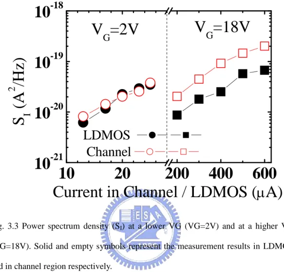
Fig. 2.10 shows a flicker noise measurement at different applied VG. Each data point represents an average of 3 to 5 devices. As VGis low (Fig. 2.10(a)), the Sid of drift region is small, which is attributed to thermal noise. In addition, the Sid of LDMOS at low VG is nearly the same as the Sid of MOS, implying that the flicker noise of LDMOS at low VGis major determined by the channel-part of the LDMOS. Compared to the I-V characteristics of Fig. 2.9(a), the ID-VI is close to the ID-VD at low VG and thus the channel region dominates the LDMOS behavior at low VG regime. At a large VG(Fig. 2.10(b)(c)), the Sidof LDMOS appears to be controlled by both the channel region and the drift region. This feature is in agreement with the comparison of I-V characteristics in Fig. 2.9(b).
The measurement result of the flicker noise behavior also implies a new characterization method for hot carrier stress. By comparing the pre-stress and post-stress flicker noise at different VG, we can identify the locations of oxide damage area in the device and corresponding trap properties. This approach will be utilized and discussed in the chapter 3
2.4 Summary
A novel metal-contact LDMOS structure is fabricated to investigate self-heating effect and LDMOS/MOS characteristics. A new technique for self-heating characterization has been proposed. This approach can probe a self-heating induced VIchange directly without adding an external resistor. The two-stage behavior of a VI transient is noticed for the first time and explained. This method provides a higher resolution than a conventional ID method. The characteristics of the channel part of the LDMOS, including the I-V characteristics and the flicker noise behaviors, are measured and compared to the LDMOS. Our measurement result shows that the drain current at low VG regime is major determined by the channel-part of the LDMOS, whereas the drain current at high VGregime is affected by both the channel region and the drift region. Similarly, the flicker noise behaviors at low VGregime and at high VG regime are controlled by the channel region and by both the channel region and the drift region, respectively.
Based on the comparison of the I-V characteristics, a new modeling methodology for LDMOS SPICE model is proposed. A two-component LDMOS model using the new methodology will be developed in chapter 5. In addition, we also proposed a noise characterization method to identify oxide damage area in various hot carrier stress modes. This method will be performed and discussed in chapter 3.
Fig. 2.1 Top view of a novel metal contact structure. Three different regions are indicated by Lch (channel region), Lacc (accumulation region), and LFOX (field-oxide region). A contact (VI) is placed in the accumulation region.
F ie ld -O x id e Ploy gate S o u rc e D ra in P-Well S u b st ra te Lch N-Well Lacc L FOX VI F ie ld -O x id e Ploy gate S o u rc e D ra in P-Well S u b st ra te Lch N-Well Lacc L FOX VI
A
A’
F ie ld -O x id e Ploy gate S o u rc e D ra in P-Well S u b st ra te Lch N-Well Lacc L FOX VI F ie ld -O x id e Ploy gate S o u rc e D ra in P-Well S u b st ra te Lch N-Well Lacc L FOX VIA
A’
Fig. 2.2 Cross-section of the metal contact structure to characterize self-heating effect. The cross-section is plotted from the line (A-A’) in Fig. 2.1. The metal contact (VI) is arranged in thebird’sbeak region with an n+implant.
S
n
+
N-Well
n
+
V
I
n
+
P-Well
Oscilloscope
Agilent 4156
D
Pulse Generator
V
G
S
n
+
N-Well
n
+
V
I
n
+
P-Well
Oscilloscope
Agilent 4156
D
Pulse Generator
V
G
Fig. 2.3 Measured internal voltage (VI) transient due to self-heating. VD is 40V. The gate voltage is switched from 15V to 40V at t=0s. Two-stage transient is noticed.
Fig. 2.4 Simulated temperature distribution along the device at VD=40V and VG=40V.
0
3
6
400
450
500
channel
drift region
T
e
m
p
e
ra
tu
re
(K
)
Position (
m)
V
G
/V
D
=40V/40V
Simulation
Fig. 2.5 (a) Internal voltage versus drain voltage with and without self-heating effect. The full squares (w/ SHE) are obtained by Agilent 4156 while the open squares (w/o SHE) are obtained from the measurement setup in Fig. 2.2. (b) Drain current versus drain voltage measured by Agilent 4156 (full squares) and by an external resistor method (open squares).
0
20
40
0
6
12
18
V
I
(V
)
V
D
(V)
w/ SHE
w/o SHE
23%
(a)
V
G
=40V
0
20
40
0
4
8
12
I
D
(m
A
)
V
D
(V)
w/ SHE
w/o SHE
8%
V
G
=40V
(b)
Fig. 2.6 Drain current versus internal voltage in a LDMOS. The reduction of VIand ID due to self-heating is denoted byVIandID, respectively.
0
6
12
18
0
6
12
I
D
I
D
(m
A
)
V
I
(V)
V
G
=40V
V
I
=23%
Fig. 2.7 ID-VD in LDMOS and in the proposed new structure. (a) At lower VG (VG<10V). (b) At higher VG(VG>10V).
0
20
40
0
1
2
3
4V
Solid: LDMOS
Empty: New Structure
I
D
(m
A
)
V
D
(V)
V
G=10V
(a)
0
20
40
0
4
8
12
16V
Solid: LDMOS
Empty: New Structure
I
D
(m
A
)
V
D
(V)
V
G=40V
(b)
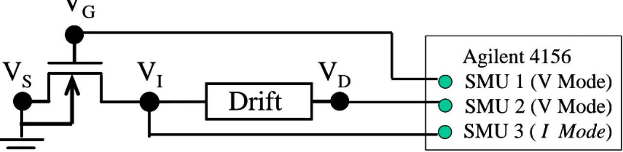
Fig. 2.8 I-V Measurement setup for device characterization. The VI is measured by forcing a zero current in SMU 3. VG/VDare given by Agilent 4156.
V
IDrift
V
DV
GV
SAgilent 4156
SMU 1 (V Mode)
SMU 2 (V Mode)
SMU 3 ( I Mode)
V
IDrift
V
DV
GV
SAgilent 4156
SMU 1 (V Mode)
SMU 2 (V Mode)
SMU 3 ( I Mode)
Fig 2.9 Comparison of metal-contact structure (ID-VD) characteristics and channel part of metal-contact structure (ID-VI) characteristics. (a) At lower VG. (b) At higher VG.
0
10
20
30
40
0
1
2
V
D
or V
I
(V)
V
G
=4V, 6V, 8V
Chanel (I
D-V
I)
I
D
(m
A
)
New Structure
(I
D-V
D)
(a)
0
10
20
30
40
0
6
12
Channel (I
D-V
I)
New Structure
(I
D-V
D)
V
G
=20V, 40V
I
D
(m
A
)
V
D
, V
I
(V)
(b)
15
20
25
10
-2210
-2110
-2010
-1910
-18LDMOS
Channel Region
Drift Region
V
G=2V
S
id
(A
2/H
z
)
I
D(
A)
(a)
0.1
0.2
0.3
10
-2210
-2110
-2010
-1910
-18(b) V
G=9V
I
D(mA)
S
id
(A
2/H
z)
10
-2110
-2010
-1910
-18(c) V
G=18V
S
id
(A
2/H
z)
Chapter 3
Physics and Characterization of Various Hot-Carrier
Degradation Modes in LDMOS by Using a Three- Region
Charge-Pumping Technique
3.1 Introduction
In recent years, multi-function power integrated chips are strongly demanded for the market of portable devices, automotive applications, and display drivers [3.1]. The integrated bipolar, CMOS, and DMOS (BCD) process has been developed to realize complex single power ICs [3.2] [3.3]. Among the candidates of high-voltage devices, lateral DMOS (LDMOS) transistors are attractive because they can be easily integrated with standard low-voltage CMOS process [3.1]-[3.4]. Nowadays, the LDMOS has been widely adopted in today’s high-voltage and high-current output circuits [3.4], from a standard 12V automotive battery [3.5] to 100V plasma display panel drivers [3.6].
One of the major reliability issues in a LDMOS is hot carrier injection and trapping in the oxide [3.7]. Since an LDMOS possesses an intrinsic channel region and a lightly doped drift region, its hot carrier degradation mechanisms are different from a traditional MOSFET. The degradation mechanisms in LDMOS are closely dependent on device dimensions, process parameters, and operation voltages. Various hot carrier stress modes have been reported for an LDMOS in literature. Different
stress conditions result in oxide damage of different types (Nitand Qox) and locations (channel or drift region). Peter Moens reported that maximum IBstress results in the worst hot carrier degradation for a gate oxide thickness from 7nm [3.7] to 17nm [3.8]. His studies showed that gate oxide damage occurs in the channel and in the accumulation regions. The device characteristics degradation is attributed to interface trap generation [3.7] [3.8]. N. Hefyene [3.9] and J.F. Chen [3.10] claimed that maximum IGstress has more serious degradation and, again, interface trap generation is the cause of degradation. Since LDMOS degradation is closely dependent on trap type and location, the profiling of trap spatial distribution and trap behavior is important to the understanding of the impact of various hot carrier stress modes.
In this chapter, we demonstrate a novel three-region charge pumping (CP) technique to probe hot carrier stress induced oxide damage in a LDMOS [3.11]. Each region of the CP current corresponds to a different part of the device. By comparing the pre-stress and post-stress charge pumping currents in each region, we are able to identify the locations of oxide damage in the device and corresponding trap properties. To further recognize the damage locations, the dependence of low frequency noise on various hot carrier stress modes will be analyzed. Based on the study of device
also studied.
3.2 Three-Region Charge Pumping Measurement
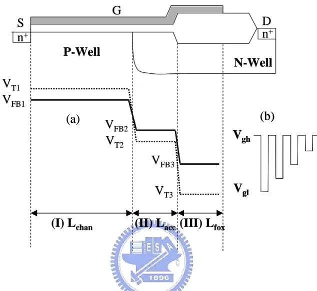
The n-LDMOS used in this work was processed in a 0.18m CMOS technology with a gate oxide thickness of 100nm and a field oxide thickness of 500nm. The operation voltages are VG=40V and VD=40V. Fig. 3.1(a) shows the device cross-section. The device is divided into three regions. Region (I) is the channel region. Regions (II) and (III) are the accumulation region and the field oxide region. The length of each region is denoted by Lchan(=3m), Lacc, and Lfox, respectively. The gate width is 20m and the threshold voltage is 1.5V.
The device flat-band voltage (VFB, solid line) and threshold voltage (VT, dash line) distributions of the three regions are illustrated in Fig. 3.1(a). In the channel region, the flat-band voltage is lower than the threshold voltage. However, in the drift region, the flat-band voltage is higher than the threshold voltage because of the n-type substrate. A lower VFB2than VFB1is attributed to the different type of substrate doping. Moreover, a higher VFB2 than VFB3 is due to a thinner oxide thickness in the accumulation region than in the field-oxide region.
The gate voltage waveform in CP measurement is illustrated in Fig. 3.1(b) with a fixed Vgh=12V and a variable Vgl. For the 100nm thick gate oxide, we can switch Vgl from +3.6V to -40V without a significant gate oxide tunneling current. In this Vgl range, all the three regions of the device can be probed. The measurement frequency in this work is 200 kHz. Typical CP measurement result is shown in Fig. 3.2. The
charge pumping current (Icp) exhibits three stages, corresponding to the three regions of a n-LDMOS respectively. It should be noticed that each stage has their corresponding threshold and flat-band voltages. By measuring the change of Icp and VFBafter stress in each stage, we are able to separate Nitand Qoxin each region of the device [3.11], for example, Nit(channel)=Icp(stage 1)/qfWLchan, Qox(acc.)=VFB (stage 2)∙C/q and so on.
3.3 Flicker Noise Measurement
Flicker noise was observed in vacuum tubes by Johnson in 1920 and interpreted by Walter Schottky in 1926. Two major models to explain the mechanisms of flicker noise in CMOS device are McWhoter’s [3.12] charge trapping model and Hooge’s empirical relation [3.13]. According to the carrier number fluctuation theory [3.12], flicker noise is explained by the fluctuation of channel free carrier where the random capture and emission by the oxide traps near Si-SiO2interface. In Hooge’s hypothesis, the flicker noise is regarded as a consequence of bulk mobility fluctuation, which is caused by phonon population through phonon scattering. However, either theory couldn’t verify the noise generation mechanism independently and completely, especially in high-voltage LDMOS.
by the channel region. At a higher VG, however, the normalized flicker noise in the LDMOS becomes lower than in the channel region because the drift region takes effect to the LDMOS. These features are similar to the device I-V characteristics in Fig. 2.3 in chapter 2 and can be used to investigate the locations of oxide damage after hot carrier stress.
3.4 Various DC Hot Carrier Stress Modes
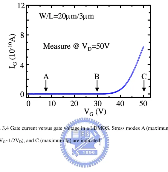
To study the dependence of damage types and locations on hot carrier stress voltages, three hot carrier stress modes, i.e., 1) mode A (maximum IB); 2) mode B (VG~1/2VD); and 3) mode C (maximum IG), are investigated. The IG-VG of a n-LDMOS is shown in Fig. 3.4. The maximum IB (mode A) stress is applied at VG/VD=8V/50V and the maximum IG(mode C) stress is at VG/VD=50V/50V. The bias conditions of the three stress modes are also indicated in Fig. 3.4. For each stress mode, the three-region CP method is performed to investigate trap type (Nit or Qox) and growth characteristics. The low-VG and high-VG flicker noise are measured to identify the damage region. Subthreshold slope and linear drain current (Idlin, @VG=40V, VD=0.1V) are used to monitor device degradation.
3.4.1 Maximum IBStress Mode
Fig. 3.5(a) shows the Icp in a fresh device and after 1400 sec. max. IBstress. The post-stress Icpin the first stage is nearly the same as the pre-stress one, indicating that region (I) oxide is not damaged by the stress. The post-stress Icp in stage 2, however, exhibits an upward shift while the flat-band voltage keeps the same (no rightward shift in the Icp). This feature suggests Nitgeneration in region (II) but no Qoxcreation. Numerical device simulation also shows the maximum IIG rate in region (II) (Fig. 3.5(b)). Although interface trap generation is observed from the Icp, the subthreshold
swing of the device is not degraded because the generated Nit is distributed in region (II) rather than in the channel region.
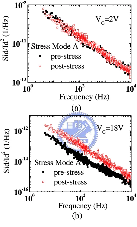
Since maximum IB stress results only Nitin region (II), the channel region is not damaged and thus the normalized flicker noise at low-VG (Fig. 3.6(a)) exhibits no significant change after stress. The damage in region (II) can be further identified by the normalized flicker noise at high-VG(Fig. 3.6(b)). The generated Nitin region (II) results in a large increase of flicker noise at high-VG but no significant Idlin degradation is observed.
3.4.2 VG~(1/2) VDStress Mode
The Icp results before and after mode B stress (@VG/VD=30V/50V) are shown in Fig. 3.7(a). Nitgeneration in stress mode B is relatively small and can be realized due to a smaller substrate current (and a smaller IIG region in Fig. 3.7(b)), as compared to stress mode A. Unlike stress mode A, a distinct flat-band voltage shift in region (II) is noticed, which is manifested by a rightward shift of the Icp in stage 2. An arrow is drawn in Fig. 3.7(a) to indicate the flat-band voltage shift (VFB2). The rightward shift of the slope is caused by negative Qox creation in region (II). Fig. 3.8 shows the evolution of the Icp with stress time. As stress time increases, the flat-band voltage of the region (II) continuously shifts to the right. The Qox2 generation rate (Fig. 3.9) can be extracted from the VFB2 versus stress time by using the equation in section 3.2.
dependence of Idlindegradation on trap location will be given later.
3.4.3 Maximum IGStress Mode
Fig. 3.12(a) shows the Icpresult before and after max. IG stress for 1000 seconds. Two different stress induced oxide degradation mechanisms are noticed; One is Nit generation in region (I) and the other is negative Qoxcreation in region (II). These two trap creation processes are reflected by an upward shift of the first stage Icp denoted by Icp1 and by a rightward shift of the second stage Icp (VFB2 in Fig. 9(a)). In contrast to stress mode A, two-dimensional device simulation reveals that the IIG region in max. IG stress splits into two parts (Fig. 3.12(b)); One is in the channel (region (I)) and the other is underneath the bird’s beak. These two degradation mechanisms are also observed in the flicker noise measurement (Fig. 3.13). The Nit generation in the channel region results an increase of the normalized flicker noise at low-VG (fig. 3.13(a)) and the oxide damage in drift region worsens the normalized flicker noise at high-VG (Fig.3.13(b)). The Nit generation in region (I) results in a significant subthreshold swing degradation (Fig. 3.14) in stress mode C. In addition, Qox2 creation accounts for a serious Idlin degradation (Fig. 3.15) in mode C. Fig. 3.15 shows that the Idlin degradation is more apparent at a larger VG. To explain the VG dependence, a two-dimensional device simulation is performed. We calculate the Idlin versus VGby placing the same amount of fixed oxide charge (Qox/q=1019/cm3) in the channel (Fig. 3.16(a)) and in the bird’s beak region (Fig. 3.16(b)). Fig. 3.16(a) shows a larger Idlin degradation at a low VG while Fig. 3.16(b) shows a larger Idlin
degradation at a high VG. The trend in Fig. 3.16(b) agrees with our measured result (Fig. 3.15) and thus we can conclude that the created Qoxis in region (II).
The Nit1 and Qox2 growth rate in stress mode C are shown in Fig. 3.17 and Fig. 3.18, respectively. The growth rate obeys a power-law time dependence and the power factor is around 0.25, which is in agreement with [3.14]. Comparing to mode A and B, the larger Qox2 growth rate in mode C is attributed to a larger stress gate current (or a higher stress gate voltage). The Idlin degradation rate is shown in Fig. 3.19. Stress mode C has the worst Idlin degradation. Due to oxide charge creation in region (II), region (II) resistance increases and the current flow in region (II) is pushed deeper. Consequently, the electron mobility exhibits a saturated effect and thus Idlin degradation has a tendency to saturate in Fig. 3.19. This mobility saturation model is also described in [3.15] [3.16] for MOSFET and [3.8] for LDMOS structure. The LDMOS degradation behavior and trap properties in the three stress modes are summarized in Table 3.1. A comparison of impact ionization generation rate distribution in the three various stress modes is shown in Fig. 3.20.
Our study reveals that the device subthreshold swing degradation is mainly affected by interface traps in the channel region while the linear drain current degradation is dictated by oxide trapped charge in the drift region. A correlation between the trap locations and the flicker noise at different applied gate voltage is noticed in the study. An increase of low-VG flicker noise accounts for the damage in the channel region and the damage in the drift region causes an increase of high-VG flicker noise. Our study also shows that maximum IBstress only results in an increase of flicker noise at high-VGand no significant Idlindegradation is observed. In addition, maximum IG stress results in the worst Idlin degradation in a LDMOS, which is attributed to both Nitgeneration in the channel region and Qoxgeneration in thebird’s beak region.
Fig. 3.1 (a) Cross-section of a n-LDMOS and flat-band (solid line) and threshold (dash line) voltage distributions. The device is divided into three parts, Lchan (channel region), Lacc (accumulation region), and Lfox (field oxide region). (b) Illustration of a charge pumping measurement waveform. The Vgh=12V is fixed and Vgl varies from +3.6V to -40V.
S
n
+N-Well
D
n
+P-Well
G
(I) L
chan(II) L
acc(III) L
foxV
FB1V
FB2V
FB3(a)
V
ghV
gl(b)
V
T1V
T2V
T3S
n
+N-Well
D
n
+P-Well
G
(I) L
chan(II) L
acc(III) L
foxV
FB1V
FB2V
FB3(a)
V
ghV
gl(b)
V
ghV
gl(b)
V
T1V
T2V
T3Fig. 3.2 Typical CP current in a n-LDMOS. The three stages of the CP current correspond to the three regions of the device. The flat-band voltage of each region is indicated in the figure. The frequency in charge pumping measurement is fixed at 200 kHz.
12
10
8
6
4
2
0
I
cp(1
0
-1 0A
)
-40
-32
-24
-16
-8
0
V
gl(V)
I
cp@ f=200kHz
D
S
L
foxL
accL
chanV
FB1V
FB2V
FB312
10
8
6
4
2
0
I
cp(1
0
-1 0A
)
12
10
8
6
4
2
0
I
cp(1
0
-1 0A
)
-40
-32
-24
-16
-8
0
V
gl(V)
-40
-32
-24
-16
-8
0
V
gl(V)
I
cp@ f=200kHz
D
S
L
foxL
accL
chanV
FB1V
FB2V
FB3Fig. 3.3 Power spectrum density (SI) at a lower VG (VG=2V) and at a higher VG (VG=18V). Solid and empty symbols represent the measurement results in LDMOS and in channel region respectively.
10
20
200
400
600
10
-21
10
-20
10
-19
10
-18
V
G
=18V
S
I
(A
2
/H
z
)
Current in Channel / LDMOS (
A)
LDMOS
Channel
V
Fig. 3.4 Gate current versus gate voltage in a LDMOS. Stress modes A (maximum IB), B (VG~1/2VD), and C (maximum IG) are indicated.
![Fig. 1.2 Applications of power semiconductor devices provided as a function of system operating frequency and power handling capability, from [1.1].](https://thumb-ap.123doks.com/thumbv2/9libinfo/8762462.208503/27.892.137.743.137.711/applications-semiconductor-provided-function-operating-frequency-handling-capability.webp)