Hl<UST PRESIDENT'S CUP 2015 FINAL REPORT
Gr~d Opt~m~zat~on of O D l~
ght~ng
Pane~ E~ectrode
Name
:
TA
NG,
Haoning
Departme
n
t
:
SENG-ECE
Supervisor:
Prof. Hoi Sing KWOK
Approval S
ig
nature:
Student
I
D
:
Y
ear
:
3
Pho
ne:
MARCH 27, 2015
Hl<USTTable
of Contents
Abstract ........................... 2
Calculation Model .................... 3
Geometry optimization Model ............................................ 5
Simulation and Data analysis based on calculation model ......... 7
t-V, L-V characteristic curve ... 7
Geometry ... 8
Current distribution on Anode ... 8
Electrode potential of grid and anode ... 9
Luminance analysis of different electrode geometries ... 11
Geometry optimization based on simulations feedback ... 11
Experiments and Data analysis ...... 13
Experiment process ...... 13 Preparation ... 13
ITO patterning ... 13
Metal sputtering and patterning ... 13
OLEO layer and Al cathode evaporation ... 13
Packaging and operation ... 13
Product ... 15
Data analysis and comparison ... 16
Future prospective ................................................................... 18
Conclusion ................................................................................... 18
Acknowledgment .......................... 18
Abstract
Organic light emitting diode (OLEO) is a display technology that will have more potential in future. However, it is essential to control the luminance, voltage losses and light uniformity that are related to the current flowing and sheet resistance of the transparent electrode panel when the size of OLED is above a cm2 [1]. One method to
optimize is to add narrow metal mesh grid to transparent electrode. The uniformity and potential wastage can consequently be improved thanks to less transmission losses on metal. The voltage losses of different shapes of grids vary from each other and it is important to find an optimal shape [1]. Our aim is to demonstrate a model on electrical properties of meshed OLED, simulated the voltage and luminance distribution to find an ideal mesh pattern and fabricated the real meshed OLED for experiment measurement.
In former studies, the potential and luminance calculation model using electro-magnetic relationship[2, 3], limit theory[4] and Poisson equation[S] has been demonstrated. This report introduces a further development of Poisson equation calculation model of current flow and voltage distribution inside the bare and meshed transparent electrode panel. A mythology of optimizing the relative luminance by inner circle radius of pattern and grid width has been demonstrated. The simulation of bare and transparent electrode panel in different shapes (square and hexagonal) among 5 geometries regarding to the voltage distribution and current flow has been done by COMSOL and MATLAB using calculation model. Then the shape parameter A that will be used in geometry optimization will be found. The result of geometry optimization and data comparison between bare and meshed transparent electrode in aspects of voltage distribution and luminance will be performed. The experiment conducted in NFF has demonstration of 4 kinds of different anode grid device will be introduced. The analysis of experimental data shows exactly the same profile with that of the simulations and provides a verification of calculation model. The plot of stages of process can be shown in Fig.1.
Verification
Models
Step 1: Calculation model
Step
2:
Optimization modelExperiments
Step
5:
Device fabricationand measurement
i
Experiment data (Compare with simulation,
optimization data)
Simulations
-+--_...
Step 3: Simulation based on calculation model...
Simulation data+
Geometry parameters+
Step 4: Optimizationsimulation based on Step 3
+
Optimization data
Fig.1 Stages of process
Calculation Model
In this project we adopt the top-bottom electrode mode in OLEO technology[6]. As for the model of electrode of OLEO with metal grid, 3 layers of elements need to be considered: non-uniform metal grid, a transparent
electrode (ITO) as anode and Aluminium top cathode, with respective thickness dg, db and dt, As can be shown in Fig.2. Assuming the cathode as ideal conductor and OLEO layer as infinite large resistor layer. The potential in bottom electrode and grid electrode can be represented by Vb(x, y) and Vg(X, y), the two values are equal. The current density in OLEO emitter layer is represented by j2, which is proportional with electric field and material conductivity. Because the thickness of 3 electrode layer is much smaller than the dimension of whole device, the model is constructed under the following assumptions[7]:
1. Top cathode is regarded as a perfect conductor that are connected to ground, which means Vt=O. 2. OLEO layer have much higher resistivity than that of bottom electrode and top electrode. Also, regarding
to the thickness of 2 electrodes, the potential and current in the electrode is considered to independent of the z-coordinate, thus we write Vb(x, y), jz(x, y).
3. For the same reason, potential is independent of z coordinate, the relationship of bottom electrode and grid can be illustrated as: Vg(x, y)=Vb(x, y).
4. Current density Jz(x, y) is a function of Vt and Vb. Jz(x, y, Vt-Vb)
.l
- ~
Yt=O_________ Al::_cathode
Vb(x, y)
Fig.2: Cross-section of OLEO device with metal cathode and transparent bottom electrode with metallic grid applied.
Current density in the electrode layers is proportional to the electric field, where[7]
j
6(x
,
y)
=
-a
b
gradV
6(x, y)
J
g
(
x,
y
)
=
-
a
g
gra
d
V
g
(x
,
y)
(1)
From these equations leads to the following set of differential equations for the electrode voltages[7]:
'v2~
(x
,
y)=
R
g
)
,
(x
,
y)v
2v;,
(x,
y
) =
Rb)= (x
,
y)
(2) (3)
(4)
Notice that the above differential equations have to be completed by boundary conditions of the following form: 1.
V/
0 ,y
0)=
Boundaryvoltage
.[8]2. Direchlet condition: boundaries of electrodes connected with a voltage source
V,,
(x
o,Yo
)=V
bo
=V
g
(x
,y
)
(5)3. Zero flux condition: boundaries of electrodes which are not contacted,
grad(V,,)
•
nb =0
(6) where nb is normal to the electrode boundary.4. In the regions (x, y} where only one electrode is present, the differential equations for the electrode voltages become "v2
V,,,1
(x
,
y)
=0
(7)In this model, we first tried to quantify jz through the linear approximation in sufficiently small voltage and current interval. Thus assuming a linear voltage[3, 6),
Solve this together with Eq. (2) and this will yields for a cylinder equation as below[7].
d
2 .d
"
r
2~ + ~ - a R r
21·
=0
(9}dr
2dr
bz
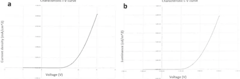
Which is a first order modified Bessel differential equation [3]. With boundary conditionjz(O)= jO, which can be find by characteristic 1-V relationship of a certain ITO material(measured in small area)[7], as shown in Fig. 6(a).
We find the solution by calculations,
(10)
Consequently, jz(x, y} can be obtained by initiating Jo(xo, yo} on the edge of electrode. Iterate jz(x,y} into~ and
the matrix of Vg(x,y) can be obtained. Setting the boundary condition~ and iterate jz(x,y} into~ we can obtain the matrix of Vb(x,y}.
The characteristic L-V curve of a certain OLEO material can be found in Fig.6(b) (measured in small area}. Simple linearization of L-V relationship is only suitable in small value applied voltage. Thus a more complicated regression
is needed in order to characterize L(x, y}. Luminance L(x, y) has a relationship with Vb(x, y}, as for small Vb(xo, yo} this relationship can be modeled by linear regression. As for large Vb(xo, yo} this relationship can be found by a polynomial regression. We see that Lis a function of Vb.
L(x
,
y)
=
k(V
6(x
,
y))*V
6(x,y)
(11)Vo(xo, yo)
l
1-V characteristic curve linear regressionjzo(xo, yo)
1
first order modifBessel differential ied equationj
z
(X,
y)
Vg(X,
y)
l(x,
y)
l
1-V characteristic curve linear and polynomial regressionVb(X,
y)
Poisson equation 1 Poisson equation 2
Direchlet boundary:Vo(x, y) Direchlet boundary:Ve(x, y) Zero flux: grad(Vb)·nb=O Zero flux: grad(Vg)·ng=O
Fig.3: process flow of simulation model
Geometry optimization Model
In this project, 2 kinds of grid shape has been discussed, square and hexagonal metal grid. As shown in Fig.4(a),
the grid width is represented by wand the inner circle radius of a unit geometry is represented by h. The top
overview of this grid pattern can be shown in Fig.4(b).
a
h
I
[
l '
-
-
-1-..-Fig.4 (a) two kinds of metal grid shape: square (left) and hexagonal (right). Parameter width (w) and height (h) are
Here we consider a square OLEO electrode with the side length
a.
Assuming that on the edge of OLEO electrodethere exists an equal potential distribution Ve. Minimum central voltage of square panel is represented by Vmin.
The total voltage drop is
t1V
=
Ve
-
Vmin
(12).Analysis the Poisson equation of voltage, it can be shown that there are 2 main reasons that resulted the losses of voltage: the voltage drop on metal grid and the voltage drop on ITO inside an element grid[2]. The voltage drop of
ITO inside an element shape is proportional to 3 parameters: jz(x, y) (Current distribution on ITO), Rb (ITO sheet resistivity) and h2 (square of inner circle radius). The voltage drop of grid is also proportional to 3 parameters: jz(x,
y) (Current distribution on grid) and Reff_g (effective grid sheet resistivity), a2 (square of OLEO electrode side
length)[7]. Thus it yields:
(13)
V
drop _grid-B*.R
-J
=
elf _ga
2 (14) (15)Where A, B is an assumed dimensionless constant. However it was found by latter simulation that for the same
shape of grid, A=B, which illustrate that A and B is only a shape depended constant. Thus,
In the calculation of luminance drop, the term of transmittance is also significant to be considered. As shown in
Fig.4 (a), the light transmittance is equal to the area of metal grid divided by total area, where w is much smaller
than h[7]:
T=(
h
)2
~1-
w (17)h+w
/
2
h
In the optimization analysis we assume that luminance is a linear function of voltage as can be shown in Fig.6 (bl
(which is acceptable for small interval voltage drop and luminance difference). Let Le be the edge luminance and
Lmin be the minimum central luminance[1]. The term in last bracket is transmittance loss. Then the following
equation can be yields:
dL
dL
.
2h
.
2 wM
=L
-L
.
=(
-
V
--(Ay
_
R
h --Ay
_
R
a
))(1--)
(18)e mm
dV
edV
-
b2w
-
gh
Eg.18 can be simplified to:
dL.
2 21
dL.
?1
h
M
=(-J_
R
w
)Au
+-
(-J_R
a
-
)Au+-
,
u
= - (19)dV
-
b2
dV
-
gu
w
u is the ratio of height and width of metal grid. There are 3 terms in Eq.19, where the first term is the loss in ITO
inside an element grid, the second term is loss on grid and the third term is related to transmittance loss[1]. To find the minimum of tiL, we calculated the first order differentiation. Usually, the second term (grid loss) is much smaller than that of first (ITO loss) and third term (transmittance loss), then ignore the second term:
dM
-(d
L
.
R
2
)2A
1
-
0
-
I1
- -
- - J
z bw
u -
- ? - ~ Uno - -dL
du
dV
u
-
3
2A(
-
·
R
w
2
)
dVl
z
bBut, if the first term can be neglected:
2
( dL .
dVl
z
R
a2)A
g
(21)
The result of Eq.20 and Eq.21 is the optimization hand w. If a further luminance loss percentage M.,
I
Le
~
6 isregulated, then under the best optimized situation[7], combine Eq.20 and Eq.18 :
462
Le dV
62L
e
dV
, -
-
-
-
s<
27
Aj
=
R
b
dL
'
-
2Aj=R
g
dL
(22}By controlling three parameters h, wands, best optimized geometry can be found. Process flow of geometry optimization can be shown in Fig.5
Vb(x,
y)'
Eq.23 characteristic function with 1-VVavg, min(Vo)
-+
t:N Simulation result of voltage A (aeometry factw)l
Eq.19 with L-V characteristic functionla"'-
mln(Vo)6l
h
(optimittd apothem)f
Simulation result ofL(x,
y)
luminanceEq.25, 26 with L=f(V) and calculated shape
parameter
1
e
(re~tlve luminance)
Fig.5 Optimization process after a run of simulation
Simulation and Data analysis based on calculation
model
FEM (finite element method)[9] was used in the simulations of this project to find the approximate solution of boundary Poisson equation problems numerically. The software used to accomplish this process is MATLAB[10]
and COMSOL multiphysics[9].
1-V: L-V characteristic curve
The 1-V and L-V characteristic curve was quantified by measuring the 1-V and 1-V relationship on a 2mm*2mm green light OLEO in lab. Since the area of device is sufficiently small, the experiment value is equal to the peak
value over the device, it is acceptable to regard the measured data as the boundary voltage and luminance of
-;; < E ~ < .§. ~ -;;; c:
..
'O...
c: !!..
::, u Characteristic 1-V curvea
Voltage (VIb
-;; < E ... ]. 8 c:..
c:e
3 Characteristic l V curve Voltage (V)Fig. 6 (a) 1-V characteristic curve of ITO that used in this project. (b) L-V characteristic curve of OLEO that used in
this project. Which is the experiment data of 1-V on2mm*2mm square OLED.
Geometry
Grid OLEDs was modeled in different geometry in Auto CAD. We have compared models for different grid shape
and boundary condition. For the convenience of experiment, a panel size of 4cm*8cm was adopted in simulations. 5 different geometries were included:
a. 4cm*8cm, Bare ITO panel
b. 4cm*8cm, 1 cm square mesh w=O.OSmm
c. 4cm*8cm, 1 cm square mesh w=O.Smm
d. 4cm*8cm,
1
cm hexagonal mesh w=O.OSmme. 4cm*8cm, 1 cm hexagonal mesh w=O.Smm
Current distribution on
Anode
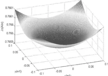
Obtaining the initial condition of Vo(xo, yo) and jzo by 1-V characteristic curve, current distribution on anode for
different marginal voltage has been simulated in MATLAB by Eq.71819, an example of current diagram (Vo=4V) can be shown in Fig.7.
0.7661 E
?
N 0.766 -, 0.766 0 7659 0.1 -0.05 0 1 y(m1) x(m1)Fig.7: Current density distribution on electrode with boundary voltage Vo=4V.
Electrode potential of grid and anode
The grid potential is simulated by iterate data of anode current distribution jz(x,y) into the Poisson
equation~-Using infinite element method in COMSOL Multiphysics with boundary condition: boundary:Vo(x, y) and zero flux
boundary: grad(Vb)·nb=O, the matrix of Vg(x, y) can be obtained. Fig.8 shows the potential drop on metal grid
when Vo=4V.
D
b
i
3897 ::,. 3fl00 389S 3893 3~2'--~--'~~~~~~~~~~~~ • ~ ~ ~ ~ o m ~ ~ ~ ~ -'{mm)Fig. 8 (a) Top view (b) side view of potential drop on metal grid when V=4V
The electrode potential drop is simulated by iterate the data matrix of Vg(x, y) into the direchlet boundary condition of Vb(x,y), with infinite element method in COMSOL Multiphysics. Fig.9 shows the potential drop on ITO electrode when Vo=4V.
D
Fig. 9 Top view of potential drop on ITO electrode when V=4V
15 data points was taken in order to calculate the average voltage and minimum voltage. The plot of average
voltage and minimum voltage versus increasing boundary voltage from 4V to lSV can be shown in Fig.10 (a)(b). It
was unable to calculate the average voltage of bare ITO electrode since the voltage of bare ITO electrode will soon
drop to zero by simulation.
10
a
Minvoltqe/~~~
/
--·-
--· -·- - - ~,.
lH Boundary Volta1e (V) VOLfD...&ridO.Smmlcm VOLE0.,.1ridO.Smmlcm_Hex -VOLED_3.9V SOA_nogrldVOLEO.,JridO.OSmmlcm VOLED_arld0.05mmlcm_liex l' ~
b
11..
I I 10 Aveni1e VolU,e ,.s us us Boundary Volta,e (V) VOLED_gridO.Smmlcm VOLED...crid0.5mmlcm_ Hex VOLED_JlridO.OSmmlcm VOLED_grldO.OSmmlcm_HexFig. 10 (a) minimum voltage and average voltage versus increasing boundary voltage from 4V to lSV for different geometries.
Luminance analysis of different electrode geometries
Minimum luminance and average luminance over the panel is quantified by Eq.11 by both linear and polynomial regression of L-V characteristic curve, based on the potential distribution data from Fig.9. The plot of minimum luminance and average luminance versus increasing boundary voltage from 4V to lSV can be shown in Fig.ll(a)(b). N° <
e
~
v·.
~ c :!!! I CO·
e
::I ~a
Min luminance II I S Boundary voltaae(V)LOIEO_gr1dO 5mmlcm LOLEO KrodO OSmmlcm
b
Avera1e lumlmince..
.,
l l Boundary Voltap (V)
-lOlEO_grldO Smmlcm LOLEO _gridO OSmmlcm
lOLED_gndO.Smmlcm_Hex -LOLEO_grldO.OSmmlcm_He•
-LITO 3 9V SOA nogrod lOLED gudO Smrnlcm_Hex LOLEO_gridO OSmmtan_tte,
Fig.11 (a)Minimum luminance and average luminance versus increasing boundary voltage from 4V to lSV for
different geometries.
It can be obtained that all geometry with hexagonal mesh shows better performance on both potential drop and luminance drop, which means this shape of mesh helps to improve the lighting performance. Comparing the result of geometries with different grid width, it can be shown that larger grid width value also provide smaller
voltage drop and luminance drop.
Geometry
optimization based
on simulations
feedback
Parameter A for different geometries and voltages can be calculated by Eq.23. According to the simulation, we found that the shape parameter A that we assumed in Eq.16 is only s shape dependent constant. That is, no matter how boundary voltage, grid height and grid width change, Ahex=0.27, Asqu=0.285, constantly. Usually,
smaller shape index indicates for a better light performance[8]:
A= (
V.,
-
~min ),Ah
ex
=
0.27
,
Asqu=
0.285
(23).
R
h
2 •R
2Consequently, height h under the condition that Rg, Rb and ware fixed and can be calculated by by Eq.20, 21 and Eq.24. The curve of dL/dV is obtained by L-V characteristic curve. The relative luminance cb with best optimized h can be calculated from Eq.26.[7] Best optimized grid height h that results in largest value of relative luminance can
then be found by the first order differentiation Eq.26, as shown in Eq.25. The relative luminance £of different geometries in former simulation can be calculated by
!).L
I
Le
.
The result of which can be shown in Fig. 12 (a).ilil,Jfl
respectively. Comparing data of Fig. 12 (bl (cl, the optimization process has certainly enhance the relativeluminance of device with the minimum relative luminance equals to 73% at Vo=lSV, while the former simulated
geometry shows minimum relative luminance equals 33% at Vo=lSV. Also notice that the optimization process
has enabled an approach between the device with square metal grid and hexagonal metal grid, while that of the
un-optimized device varies a lot.
a
0?1, 0.01 0 Hh=u
,ro
*w
(24)de
b
=-2(dL i
z
R
b
w
2)A!!__+.::!...=O=}h
(
2s)dh
dV
Le
w2
h
2
0µ11111,zed 6=
l
-
!iL
=
l
-(
dL
ix
R
b
w
2)A(!!:_
)2
_
(
dL
i:Rga
2)A!!:__
w
Le
dV
Le
w
dV 2Le
w
h
(26)Optimization of h under w::0.Smm
c
Relative luminance for different geometries"•
N < E ... 9S llS IH Boundary voltage (V) ISSh. hex -h_squ
"'C
~
.,
u c:
b
Relative luminance with best optimized h"'
c:·
e
0.97 II I.I ) c: ta c:·
e
~ II > ;; ..!! Ill O 11 a: 0 ·, 's I 11 Boundary Voltage (V) - e_hex e_,qu :, -' o• 0 l!, ! I Boundary Voltage (V) -e_grldO.Smmlcm - e_gridO.Smmlcm_Hex e_t,ridO.OSmmlcm e_gridO OSmmlcm_HexFig.12 (a) Optimized h with constant w versus increasing boundary voltage from 4V to 15V. (b)Relative luminance
E:b with best optimized h versus increasing boundary voltage from 4V to 15V. (c) Relative luminance E: of different geometries in former simulation versus increasing boundary voltage from 4V to 15V.
Experiments and Data analysis
Experiment process
The experiment was conducted in HKUST Nanoelectronics Fabrication Facility and CDR after the safety training.
Preparation
ITO glasses with sheet resistance equals to 25
Q
/0
is firstly need to be cut into 10cm*10cm pieces. The cut glass will be washed by ultrasonic tank and liquid soap tank to ensure the cleanness before entering NFF. The wholeprocess in NFF is non-CMOS process.
ITO patterning
The first step is to coating resist on ITO glass, the equipment used is SUSS Manual Resist Spin Coater with
photoresist # 503, the thickness of photoresist is controlled to 1-2um. A soft bake is needed after spin coating on hotplate for 1.5 min, as can be shown in Fig. 13 (a).
The second step is to expose ITO glass in UV light by Contact Aligner AB-M#2(UV}, the exposure time is 1 min.
The third step is to develop the pattern in FHD-5 solution for 1 min, after which a 1 min rinsing process is need in wet station. A hard bake in furnace is needed after the developing step for 120min, as can be shown in Fig.13 (b).
The fourth step is to etch away exposed ITO by nitrohydrochloric acid in wet station El for 20 min. The remaining
photoresist that were protecting ITO from nitrohydrochloric acid will be lift off by acetone in wet station E4 for 2
min. Final rinsing process by DI water is required by 5min. Fig. 13 (cl shows a simple lustration of how positive photolithograph process was conducte.
Metal sputtering and patterning
If Cu is used as anode metal grid, we will use the sputter or CVD method by equipment
eve
602 Sputtering Systemor Cooke E-Beam Evaporation System, respectively. As can be shown in Fig. 13 (d). Metal grid patterning is needed
after the deposition process using specific mask, which is quite similar to the ITO patterning process, the example
of masks for light exposure can be shown in Fig.14 (al (b). The little differences is that in fourth step of patterning,
we etch away Cu by chromic acid in wet station El for 1 min, as shown in Fig. 13 (e).
If Al is used as anode metal grid, it will be evaporated together in the OLEO layer evaporation step, the pattern will
be etched away bye-beam. Fig.13 (fl (g) is the diagram of patterned hexagonal and square metal grid.
However, the resistances of same metal using different method of deposition always vary with each other. It is
significant to find a convenient way of deposition at the same time, relatively low resistance should be ensured. OLED layer and Al cathode evaporation
As in Fig.13 (k), the OLEO organic layer will be deposited on anode after anode fabrication, which is the main
working part of an OLEO device. In this project, we fabricate green light OLEO for process convenience. OLEO layer
is evaporated in evaporation chamber. As can be shown in Fig. 13 (m), in first chamber, 6 organic layers include:
HATCN (hole injection layer) for 200nm, NPB (hole transport layer) for 40nm, 6wt% lr(ppy)3: CBP (emitting layer) for 20nm, BAlq (hole blocking layer) for 5nm, Alq3 (electron transport layer) for 40nm, LiF (electron injection
layer) for lnm. Al top cathode is fabricated in second metal chamber, as shown in Fig. 13 (I).
Packaging and operation
The packing process in conducted in glove box with 16 pieces of desiccative stick on the backside of device. So far,
this process has never been success. As shown in the complete device structure in Fig. 13 (1), the 2 panel of OLEO
is in paralleling relationship. Thus, same voltage will be applied on 2 areas one we connect 2 terminal electrode.
\
Fig. 13 (a) ITO glass with PR spin coated. (b) Photolithograph of ITO. (c) Illustration of photolithograph process. (d) Sputtering metal on plate. (e) Photolithograph of metal. (f) Patterned hexagonal metal grid. (j) patterned square metal grid. (k) Evaporate organic layer on anode. (i) Evaporate Al cathode. (m) Layer structure of OLEO layer, (n)
equipment used in NFF.
Fig.14 Example of shadow mask used in the process of photolithograph.
Product
When fabricated large panel OLED as shown in process flow above. The figures of product can be shown in Fig.15, where (a) to (d) are the successful products operating in lab. Large area OLED lighting panel is hard to be made in
NFF mainly because of the defects occurs during the metal and photo-resist etching process and the deposition of
organic layer, also the material we used have certain variations comparing to the parameters we set in
simulations. Short circuit effect and thermal effect will be caused once there is a defect dot on OLED panel, as the
result, whole device will be broken[11, 12]. To avoid this, a higher level of cleaning and a precise time control are
required. It was found that inserting metal grid in ITO anode reduce the chances of short circuit effect and thermal
effect because of a higher effective conductivity, the device life time was also found to be longer.
Fig.15 Sample product of (a) Bare ITO electrode. (b) ITO electrode with outer Al grid. {c) Square Al grid, w=O.Smm,
h=7mm. {d) Hexagonal Al grid, w=O.Smm, h=7mm. (e) Dots of defect on OLED panel. (f) Defects image under the
The measurement of L-V data was done by SpectraSacn 650. with voltage source changing from 5V to 15V, we
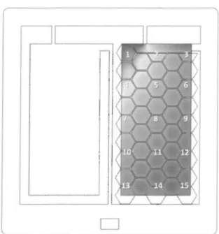
take the value of luminance on a specific point on the OLEO panel. 18 points was taken on each pieces of OLEO panel.
Data analysis and
comparison
We compared 4 kinds of OLEO panel with different electrode geometry in experiment. a. Bare ITO electrode
b. ITO electrode with outer Al grid c. Square Al grid, w=O.Smm, h=7mm d. Hexagonal Al grid, w=O.Smm, h=7mm
The geometry of these 4 kinds of samples can be shown in Fig.16.
b
Fig.16 (a) Bare ITO electrode. (b) ITO electrode with outer Al grid. (c) Square Al grid, w=0.5mm, h=7mm. (d) Hexagonal Al grid, w=O.Smm, h=7mm
Luminance data allocated by SpectraSacn 650. The number of data points that has been taken is 18 in the efficient lighting zone of OLEO panel. Fig.17 shows the luminance distribution along different data points on 4 metal grid geometry. The highest luminance value is the maximum luminance value over the panel, which can be regarded as the edge luminance in latter calculations. The peak value of luminance indicate the points that are nearing to anode and the valley value on curve indicate the middle point on OLEO panel. Maximum, minimum, average and relative luminance of experiment samples, as shown in Fig.18, has verified the simulations result that hexagonal
metal grid shows better proformance than square aquare metal grid.
However, the absolute value of maxmum, minimum and average luminance from experiment data is relatively low than simulations. This is considered to be the potential losses on the contact interface of voltage source and OLEO electrode and the surface defects on organic layer. Although the value of luminances are lower than that of simulated samples, the relative luminance calculated by Eq.26 gives a reasonable result with 61% to 76% for hexagonal electrode panel. Comparing Fig.18 with Fig.10,11, we see that the profiles of minimum, average and
relative luminance of simulated and experiment data are similar and the highest value of relative luminance is
roughly close to that of the optimized simulation, which proves a good verification that of model is feasible in the study of OLED electrode panel.
"""''
160l.CJ.[I]
a
7·n.cub
t P .. 01 Outer metal gridN •r·t•J ;::; t )t)f•Ol < E 6V < E -=c, ~H ... '.tO, av ... 10.{·0J 6V ,!(.
.,,
u av 41 •OCf ').I 10V '.; u....
..,
c..,
10V..
s:: H>Ct:•OJ 12V c..
·
e
c....
.,
12V -14V·e
3 ltl.1.QJ -15V .3 1 OOf*O) -14V •.U ,l,;)t_~J 15V Q,~f•" OID-cl> 0.
.
.
"
"
"
,.
0...
"
••
••
••
data point data point
40Jf.01 IQ,GJ
rn
c
l,_.,.,,
Square metal eridd
Hex metal grid \('Ii ,OJ N \0::,01 .:, < < E 6Ve
41.lil ·n ~ )IO(, ... ... 6V -0 ~.,
BV ~ ·8V """Ol 8 ..)( f· u lOV c c 10V ~ 1',t,o, UV"'
c: 12V·
e:
:, ClH..(JJ - 14V·e
:,.., ..,,
- 14V ..., ..., 15V··
Ol
15V .... , .. u, O<X>!-<TI 0"1 ••.
.
"
..
..
,
,,
.
,
..
,
.
..
data point data point
Fig.17 Luminance distribution versus data points on (a) Bare ITO electrode (b) ITO electrode with outer Al grid (c)
Square Al grid, w=O.Smm, h=7mm (d) Hexagonal Al grid, w=O.Smm, h=7mm
a
- \<W N <!..
1• "O ~ ii.I '"l)O v c..
C ,oo,e
:, .., l:ol Max Luminance Boundary Voltage (V)-mu(HE><I -max(SQU) mer(Metal ~· d)
b
. .,..,
;::;-E
..
.,
... ]. ... )' ill..,
c •."'
c:e
.3 ' l l Boundar Voltage (V}-mon(HEX; -m,n(SQU) min(M~tal grid) 1) m.ix(ITO only) !I !'Tl°'1(lTO only)
c
Averaee Luminance 11 u Boundary Voltage (V)-avg(HEX) - a v0(Sj ) ,._. al •Id) avc(ITO onlv)
d
o,
Relative Luminance ;::;-< E-
"O ~ ~ ill ~ OJ.\"'
c: o.•·
e
:,..,
Q<....
,s 1• 10~ II~ U'"
• s Boundary Voltace (V}Fig.18 (a) Maximum luminance (b) Minimum luminance (c) Average luminance (d} Relative luminance of OLEO panels with 4 different electrodes versus increasing boundary voltage from 4V to lSV.
Future prospective
In aspect a model construction, we hoped to find a functional relationship between device side length
a
and relative luminance with constantw,
hand R parameters. This relationship has not been presented yet because the simulation software was unable to hold large data point calculations. The simplification of quantification model will help to realize the simulation.In aspect of experiment, one main problem to solve is the packaging of OLED device. Since raw OLEO material is unstable in humid air condition, it will break down fast without packaging. Our packaging process for large panel OLEO will somehow disable the device. In order to get a more reliable data, the optimization of packaging process necessary.
Conclusion
In this project, we have firstly constructed a calculation model for the voltage distribution and luminance drops on a bare or grid patterned OLEO lighting panel. A mythology of optimizing the relative luminance by the pattern inner circle radius and grid width has been demonstrated. Simulations based on the calculation model with free set of parameters was done in order to find the shape parameter A that will be used in geometry optimization, also the best geometry hexagonal shape was found among 5 geometries. The result of geometry optimization by feedback parameters has been demonstrated by simulations, which shows a good result of 73% relative luminance in largest boundary voltage. The experiment conducted in NFF has demonstrated 4 kinds of different anode grid device. A process flow of experiment and the method of data measuring have been introduced. The experimental data shows exactly same profile with that of the simulations, which verified the feasibility of our calculation model.
Acknowledgment
Thanks to the instruction of Prof. KWOK. Also thanks to the guidance and help from Mr. Yibin, JANG and Mr. He, Li and all the group members in Prof. Kwok's group.
Reference
(1) K. Neyts, M. Marescaux, A. U. Nieto, A. Elschner, W. L6venich, K. Fehse, et al., "Inhomogeneous luminance in organic
light emitting diodes related to electrode resistivity," Journal of Applied Physics, vol. 100, p. 114513, 2006.
[2) M. Slawinski, D. Bertram, M. Heuken, H. Kalisch, and A. Vescan, "Electrothermal characterization of large-area
organic light-emitting diodes employing finite-element simulation," Organic Electronics, vol. 12, pp. 1399-1405,
2011.
(3) B. J. Roth, N. G. Sepulveda, and J.P. Wikswo, "Using a magnetometer to image a two-dimensional current
distribution," Journal of Applied Physics, vol. 65, p. 361, 1989.
(4) L. Pohl, Z. Kohari, and
v.
Szekely, "Fast field solver for the simulation of large-area OLEDs," Microelectronics Journal,vol. 41, pp. 566-573, 2010.
[SJ Y. Galagan, J.-E. J.M. Rubingh, R. Andriessen, C.-C. Fan, P. W.M. Blom, S. C. Veenstra, et al., "ITO-free flexible organic
solar cells with printed current collecting grids," Solar Energy Materials and Solar Cells, vol. 95, pp. 1339-1343, 2011.
[6) K. Tvingstedt and 0. lnganas, "Electrode Grids for ITO Free Organic Photovoltaic Devices," Advanced Materials, vol.
19, pp. 2893-2897, 2007.
(7) K. Neyts, A. Real, M. Marescaux, S. Mladenovski, and J. Beeckman, "Conductor grid optimization for luminance loss
reduction in organic light emitting diodes," Journal of Applied Physics, vol. 103, p. 093113, 2008.
(8) M. Slawinski, M. Weingarten, M. Heuken, A. Vescan, and H. Kalisch, "Investigation of large-area OLEO devices with
various grid geometries," Organic Electronics, vol. 14, pp. 2387-2391, 2013.
(9) A. Comsol, "COMSOL multiphysics user's guide," Version: September, 2005.
[10) M. U. s. Guide, "The mathworks," Inc., Natick, MA, vol. 5, p. 333, 1998.
(11) J. W. Park, T. W. Kim, and J. B. Park, "Investigation on a short circuit of large-area OLEO lighting panels,"
Semiconductor Science and Technology, vol. 28, p. 045013, 2013.
(12) J. W. Park, D. C. Shin, and S. H. Park, "Large-area OLEO lightings and their applications," Semiconductor Science and