62 IEEE TRANSACTIONS ON DEVICE AND MATERIALS RELIABILITY, VOL. 10, NO. 1, MARCH 2010
Characterization of the Channel-Shortening
Effect on P-Type Poly-Si TFTs
Ya-Hsiang Tai, Member, IEEE, Shih-Che Huang, and Po-Ting Chen
Abstract—The phenomenon of channel shortening for p-type
poly-Si thin-film transistors (TFTs) after stress is studied in this paper. Increased mobility, shifted threshold voltage VTH, and
reduced leakage current for the stressed device are observed. In addition, the capacitance–voltage (C –V ) behavior for the stressed device exhibits the anomalous increase for the measuring gate voltage in the OFF region. A model illustrating how the trap electron mechanism would occur is provided. Furthermore, the degradation behavior of the p-type poly-Si TFT under gate ac stress in the OFF region is also studied. Similar degradation behaviors are observed for the gate-ac-stressed TFT for both of their I–V and C –V characteristics. A distributed device circuit model is proposed, and based on this model, it is proposed that the main voltage drop during gate ac stress in the OFF region could occur at the source and drain junction, which may, in turn, degrade the device. A gated p-i-n device under the same process condition is then adopted and dc stressed to verify the proposed mechanism. The similarity between the capacitance curves for the ac-stressed TFT and the dc-stressed gated p-i-n device proves the validity of the proposed mechanism.
Index Terms—AC stress, capacitance–voltage (C –V ), channel
shortening, hot-carrier stress, poly-Si thin-film transistor (TFT), reliability.
I. INTRODUCTION
D
UE to their high mobility and capability of forming both in-pixel switches and integrated-circuit elements on the same glass, low-temperature-poly-Si (LTPS) thin-film transis-tors (TFTs) have attracted much attention for active-matrix liquid-crystal-display and active-matrix organic-light-emitting-diode applications [1]. The reliability behavior of poly-Si TFTs would be a critical issue for the applications. The main reliabil-ity issues for poly-Si TFTs under dc operation are hot-carrier and self-heating effects [2]. Referring to previous works, there are many papers reported on the degradation mechanisms of the current transfer behaviors, namely, the ID–VG curves, and thecapacitance–voltage behaviors for n-type poly-Si TFTs under
Manuscript received June 4, 2009; revised August 1, 2009 and September 11, 2009. First published October 20, 2009; current version pub-lished March 5, 2010. This work was supported in part by the National Science Council, Republic of China, under Grant NSC 98-2218-E-009-004 and in part by the Ministry of Economic Affairs through the Technology Development Program for Academia, Taiwan, under Contract 96-EC-17-A-07-S1-046.
Y.-H. Tai and P.-T. Chen are with the Department of Photonics and the Display Institute, National Chiao Tung University, Hsinchu 30010, Taiwan (e-mail: [email protected]; [email protected]).
S.-C. Huang is with the Department of Photonics and the Institute of Electro-Optical Engineering, National Chiao Tung University, Hsinchu 30010, Taiwan (e-mail: [email protected]).
Color versions of one or more of the figures in this paper are available online at http://ieeexplore.ieee.org.
Digital Object Identifier 10.1109/TDMR.2009.2033466
various stress conditions, while there are few papers for p-type Si TFTs [3]–[7]. On the other hand, because poly-Si TFTs have the capability of forming integrated circuits, the devices may be operated under gate pulses toggling in the ON and OFF regions at high frequency or, for some period, even in the OFF region alone. The reliability behavior for both n-and p-type poly-Si TFTs operating between the ON n-and OFF regions was reported by Uraoka et al., and we had reported the reliability behavior for the n-type poly-Si TFTs operated in the OFF region [8]–[10]. However, there are very few reports on the reliability of the p-type poly-Si TFTs dynamically operated in the OFF region. In this paper, for the dc hot-carrier effect on the p-type poly-Si TFTs, the ID–VGcurves, the corresponding
transconductance curves, and the C–V curves are studied and discussed. For the device that is gate ac stressed in the OFF region, the ID–VG curves, mobility increase, and the C–V
curves are also examined. A device circuit model is proposed, and based on the model, the gated p-i-n device is utilized and stressed to verify the proposed mechanism.
II. EXPERIMENTALDETAILS
Top-gate LTPS TFTs with width/length of 20 μm/5 μm were fabricated using a low-temperature process. First, the buffer oxide and a-Si:H films with thickness of 50 nm were deposited on glass substrates by plasma-enhanced chemical vapor depo-sition (PECVD). The samples were then placed in the oven for dehydrogenation. The XeCl excimer laser of wavelength of 308 nm and energy density of 400 mJ/cm2 was applied. The laser scanned the a-Si:H film with a beamwidth of 4 mm and 98% overlap to recrystallize the a-Si:H film to poly-Si. After poly-Si active-area definition, 50-nm SiO2 and 25-nm SiNX
were deposited with PECVD as the gate insulator. Next, the TFT gate was formed by metal sputtering and then defined by photolithography. P+ source/drain doping was done by B
2H6 self-aligned implantation with a dosage of 2× 1015 cm−2. Then, the interlayer of SiNX was deposited. Subsequently,
dopants were activated via rapid thermal annealing, while the poly-Si film was hydrogenated simultaneously. Finally, contact-hole formation and metallization were performed to complete the fabrication work. The slight difference between the gated p-i-n device process and the p-type TFT process is that one side of the source/drain doping was changed to n− and n+, which are of dosages of 2× 10¹³and 2× 1015cm−2of PH3, respectively. The gated p-i-n devices are fabricated in parallel with the TFTs on the same glass substrate to ensure identical process conditions. The typical values of the threshold voltage for p-type fresh devices are−1.88 V.
TAI et al.: CHARACTERIZATION OF THE CHANNEL-SHORTENING EFFECT ON P-TYPE POLY-Si TFTs 63
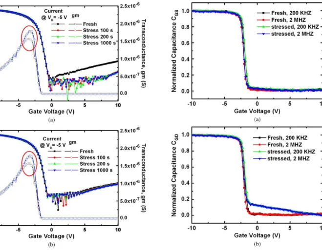
Fig. 1. ID–VGand transconductance curves for the device before and after
stress in (a) forward connection and (b) reverse connection.
The rectangular pulses applied to the TFTs are generated with an Agilent 41501B pulse generator, and dc stress is performed by using an Agilent 4156A precision semiconductor parameter analyzer. The capacitance–voltage (C–V ) curves are measured with an Agilent E4980A precision LCR meter.
III. DISCUSSION
A. DC Stress
The hot-carrier effect, as many had reported, is closely related to the electric-field distribution near the drain side and is therefore closely related to the applied gate voltage VGS and drain voltage VDS. Because the active region of poly-Si TFTs is composed of grains, the hot-carrier effect may be even more complicated than that in MOSFETs. Unlike that in MOSFETs, the hot-carrier effect in TFTs becomes most severe as VGS is just above its threshold voltage VTH and as VDS is large [11]. Fig. 1(a) shows the ID–VG and transconductance
curves in the forward connection before and after stress, while Fig. 1(b) shows those in the reverse connection. Here, “for-ward connection” means that, in stress, the source and drain connections are the same as those during measurement, while “reverse connection” means that they are swapped. The stress condition is that VDSis equal to−20 V and that |VGS| is around 1 V larger than|VTH|, namely, −3 V. Different from the hot-carrier effect on n-type poly-Si TFTs, the performance of p-type
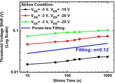
Fig. 2. (a) Normalized gate-to-source-capacitance CGS curves and
(b) normalized gate-to-drain-capacitance CGDcurves for the device before
and after 200-s stress.
poly-Si TFTs after stress actually improves [12]. Referring to Fig. 1(a) and (b), both in the forward and reverse connections, the peak value of transconductance after stress increases with the ratio of around 10% as compared to that of the fresh device. Moreover, in the forward connection, the leakage current of the stressed device shows an apparent decrease by one order of magnitude for VGSthat is equal to 10 V. However, the leakage-current decrease is not observed in the reverse connection. The difference between Fig. 1(a) and (b) may reveal that stress could affect differently for the source and drain junction.
In order to understand the explicit mechanism about the hot-carrier stress, the capacitance–voltage (C–V ) behaviors are also measured. Different from MOSFETs, because there are no back electrodes for TFTs, one may only measure the C–V behavior through the gate-to-source connection or the gate-to-drain con-nection. Nevertheless, such connections can still provide useful information around the source and drain junctions. Fig. 2(a) and (b) shows the normalized gate-to-source-capacitance CGS and gate-to-drain-capacitance CGDcurves for the device before and after stress with different measuring frequencies, respec-tively. The CGS curves are measured with the floating drain, while the CGD curves are measured with the floating source. The normalized capacitance is the ratio of the measured capac-itance to the gate-insulator capaccapac-itance of the TFT. The stress condition is the same as the previous condition, namely, stress
64 IEEE TRANSACTIONS ON DEVICE AND MATERIALS RELIABILITY, VOL. 10, NO. 1, MARCH 2010
Fig. 3. Mobility increase for poly-Si TFTs under different stress conditions.
VDS is −20 V, and VGS is −3 V with a stress duration of 200 s. Referring to Fig. 2(a), the CGScurves after stress show almost no change as compared to those before stress. However, the CGD curves after stress, as shown in Fig. 2(b), show an anomalous increase for the gate voltage in the OFF region. Because, in this region, there should be no inversion layer formed, the capacitance curves should be zero in this region. The capacitance-curve increase could come from the stress-induced state creation or charge trapping. However, as shown in Fig. 2(b), this increase is the same for both the high and low measuring frequencies, which indicates that the increase can be attributed to the trapped charges instead of states because states would respond to different measuring frequencies and result in dispersion behavior in the C–V curves [13]. Meanwhile, because the device is partially turned on, it may be inferred that there are certain amounts of holes induced beneath the gate when the device is in the OFF region. Therefore, it may be inferred that the dominant mechanism under such stress condition is the electron trapping in the gate insulator near the drain region instead of hole trapping.
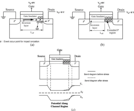
Fig. 3 shows the mobility-increase ratio of the p-type TFT with different stress VDS’s, and Fig. 4 shows that for the threshold-voltage shift. The threshold-voltage shift here is de-fined as follows: VTH (stressed)–VTH (fresh). As shown in both figures, mobility-increase ratio and threshold-voltage shift show power dependence with stress time. The curves are fitted with power–time dependence Atn, and both A and n are
con-stants. The fitting curves, as well as the fitting parameter n, are given in the figures. Furthermore, as stress VDSincreases, both device parameters show larger change. Such power-law–time dependence for the device parameters and the dependence on stress drain voltage are similar to the channel-shortening ef-fect, or the hot-electron-induced punchthrough efef-fect, in p-type MOSFETs [14]–[16]. Referring to the bulk p-type MOSFETs, the same fitting equation is used, and the fitting parameter n for
VTH shift is about 0.1–0.7. It is shown that, if the exponent is 0.1–0.3, the degradation mechanism is carrier trapping in the gate oxide, while if the exponent is 0.3–0.7, the mechanism could be attributed to interface-state creation at the Si/gate oxide interface [15]. Back to our study, the fitting exponent for VTH shift falls in the 0.1–0.3 region, indicating that the
Fig. 4. VTHshift for poly-Si TFTs under different stress conditions.
dominant mechanism should be charge trapping in the gate insulator instead of interface-state creation. Such an inference is also consistent with the aforementioned C–V measurement for the device before and after stress with different measur-ing frequencies. However, in p-type MOSFETs, the leakage-current reduction and the anomalous CGD-curve increase are not observed. This may be attributed to the structure difference between MOSFETs and TFTs. In addition, because the poly-Si film is composed of large amount of grains and it is reported that the hot-carrier effect is related to the grain structure near the drain region, the existence of grain boundary may also contribute to such difference [17].
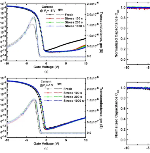
A proposed model describing the channel-shortening effect in the p-type poly-Si TFT under dc stress is shown in Fig. 5. During stress, as shown in Fig. 5(a), channel carriers may attain sufficiently high energy and then become hot carriers. These highly energetic carriers may then interact with the lattice, and the event of impact ionization could occur near the drain side, generating electron–hole pairs, as shown in the figure. The impact-generated holes would mainly be collected by the drain electrode because, for holes, the energy barrier between the gate insulator and the poly-Si film is too high to inject into the gate oxide. On the other hand, the generated electrons could possibly move toward the substrate, the source side, or the gate electrode because of the electric-potential distribution during stress. As in the case of p-type MOSFETs, the substrate current, mainly con-tributed by the impact-ionization-generated electrons, provides the information and “signature” of the behavior of the impact-ionization event in the channel [18], [19]. However, because there is no substrate electrode for TFTs to discharge these electrons, the possibility for the electrons to move toward the gate dielectric is higher, and one may only examine the device performance after stress because there is no such substrate current to study. These electrons could then get trapped in the gate-dielectric film and help induce holes near the drain side, equivalently forming the lightly doped region beneath the gate-dielectric region in the following measurement, as shown in Fig. 5(b). In this way, the effective channel length is shortened, which gives rise to the changes of mobility and threshold voltage after stress, just as in the case of p-type MOSFETs
TAI et al.: CHARACTERIZATION OF THE CHANNEL-SHORTENING EFFECT ON P-TYPE POLY-Si TFTs 65
Fig. 5. Device model for p-type poly-Si TFTs (a) during stress, (b) after stress, during measurement, and (c) corresponding band diagram.
under hot-carrier stress. Such a similarity can also be observed from the power–time dependence between Fig. 3, Fig. 4, and [14]. However, it has never been reported for the capacitance behavior and the leakage-current reduction of the p-type poly-Si TFT after such a stress. As for the capacitance behavior, the CGS curves after stress show no change because there is no trapped charge in the gate dielectric near the source side. For the CGD curves, because of the trapped charges in the insulator on the drain side, the surface-potential distribution of the poly-Si film beneath the trapped electron region would be altered because of these electrons. For the applied gate voltage
VGS is still in the OFF region, −1 V for example, the band bending of the poly-Si film beneath the trapped electrons could be sufficient to reach the inversion region with the help of the trapped electrons, while other regions in the channel may still in the accumulation or the depletion region. At this time, the inversion charges would only partially appear near the drain junction for VGS before the flatband voltage and form such a partially turned-on capacitance behavior.
The leakage-current behavior of poly-Si TFTs is quite dif-ferent from that of MOSFETs. Although they are of the same structure, the leakage-current behavior of poly-Si TFTs is mainly dominated by the depletion behavior near the drain side [20]. As in the case of this paper, the trapped electrons in the gate insulator on the drain side, resulting from the impact-ionization effect, would help induce more holes in the region beneath the gate. This acts like a p− region in the channel and essentially becomes a one-side gate-overlap lightly doped drain (GOLDD) structure. This changes the behavior of the band diagram near the drain side while the source side remains unchanged, as shown in Fig. 5(c). The localized p− region relieves the electrical field near the drain side just like the GOLDD structure, and therefore, the leakage-current behavior is relieved [21]. Because only the band diagram near the drain
side is altered while that near the source side is unchanged, such a leakage-current-reduction behavior is only observed in the forward connection but not in the reverse connection. Such a behavior is not observed in p-type MOSFETs be-cause the dominant leakage behavior for poly-Si TFTs comes from the drain-side depletion region, whereas that behavior for MOSFETs is dominated by the punchthrough and GIDL current under such a gate-voltage region [22]. The characterization of the channel-shortening effect after hot-carrier stress, like the device performance and the leakage behavior after stress, would help designers in designing the circuit with better understanding of device reliability and circuit performance under various operation conditions.
B. AC Stress
Poly-Si TFTs, in the past decade, attracted much attention because its high device mobility enables many new applications [23]. One main application of poly-Si TFTs is the integrated circuits of the display panel. These TFTs in the driver circuits are subjected to high-frequency and high-voltage ac operation. In such a case, the reliability behavior of poly-Si TFTs becomes a critical issue in designing the circuit and the corresponding operation conditions. The reliability of poly-Si TFTs toggling between the ON and OFF regions was reported by Uraoka et al., in which the degradation of poly-Si TFTs is found to be closely related to the transient region of the applied gate pulse because the discharge behavior of the channel carriers in poly-Si TFTs is quite different from that in MOSFETs [8]. However, there are very few papers on the reliability of poly-Si TFTs under gate ac operation in the OFF region. We reported previously the reliability behavior of n-type poly-Si TFTs under gate ac stress in the OFF region, while there is no paper so far about that of p-type devices [10]. In the following discussion, the I–V
66 IEEE TRANSACTIONS ON DEVICE AND MATERIALS RELIABILITY, VOL. 10, NO. 1, MARCH 2010
Fig. 6. ID–VGand transconductance curves for the device before and after
(a) gate ac stress and (b) gate dc stress.
and C–V behaviors of poly-Si TFTs under gate ac operation in the OFF region are examined. In comparison, the reliability behavior of devices under gate dc operation in the OFF region is also studied.
Fig. 6(a) shows the transfer-characteristic curves for the p-type poly-Si TFT before and after stress. The stress condition is that the gate ac signal toggles between 0 and 20 V with a duty ratio of 50% at 500 kHz and that the source and drain electrodes are grounded. Referring to this figure, the transfer behavior of the device after stress shows improved device performance, such as increased mobility, decreased leakage current, and slightly shifted VTH in the positive direction. Such a performance improvement is just similar to the effect of channel shortening, as described in the previous section. However, in this case, during stress, there should be no channel carriers because the applied gate voltage is toggling in the OFF region. In comparison, the transfer behavior of p-type poly-Si TFTs under dc operation in the OFF region is shown in Fig. 6(b). The stress condition is that the stress gate voltage is dc 20 V and that the source and drain electrodes are grounded. The transfer curves for the device after such a stress show an apparent VTH shift in the positive direction, which could be similar to the case of gate ac stress in the OFF region, as shown in Fig. 6(a). However, the mobility and leakage behavior after stress show almost identical behaviors as compared to that of the fresh device, which is very different from Fig. 6(a). This
Fig. 7. Normalized capacitance curves for the device before and after (a) gate ac stress and (b) gate dc stress for 200 s.
may reveal that the dominant mechanism for p-type poly-Si TFTs under gate ac stress in the OFF region could be very different from that under gate dc stress.
In order to find a more explicit understanding of the domi-nant mechanism, the corresponding capacitance behaviors are measured. Fig. 7(a) shows the normalized capacitance curves of the device under gate ac stress, while Fig. 7(b) shows that under gate dc stress. The stress condition of Fig. 7(a) is just the same as that of Figs. 6(a), and the stress condition of Fig. 7(b) is the same as that of Fig. 6(b). Both stress conditions last for 200 s. As for Fig. 7(a), the capacitance curves show an apparent increase for the gate voltage in the OFF region, and this increase is the same for different measurement frequencies, which is just similar to the behaviors shown in Fig. 2(b). On the other hand, as shown in Fig. 7(b), the C–V curves for the device after gate dc stress show only a slight VFBshift as compared to the curves before stress. This reveals that, once again, the degradation behaviors for the device under gate ac and dc stresses in the OFF region are very different.
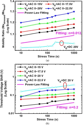
Fig. 8(a) shows the mobility increase of p-type poly-Si TFTs under gate ac and dc stresses, while Fig. 8(b) shows the threshold-voltage shift after stress. As shown in Fig. 8(a), the mobility increase of the device after ac stress also shows the power-law–time dependence, as in the case of dc hot-carrier
TAI et al.: CHARACTERIZATION OF THE CHANNEL-SHORTENING EFFECT ON P-TYPE POLY-Si TFTs 67
Fig. 8. (a) Mobility increase and (b) threshold-voltage shift for the device under gate ac and dc stresses with different gate-pulse levels.
stress, and such a mobility increase can be as high as 30% when the operation time reaches 1000 s. Such a power–time dependence is also fitted with the same equation Atn, and the fitting curves, as well as the fitting parameter n, are shown in the figure. In addition, such an increase apparently depends on the applied gate voltage, although the applied voltages all fall in the OFF region. The mobility increase for the device after gate dc stress in the OFF region is also shown in the figure. The mobility increase under such an operation is less than 5% and shows no apparent relation with stress time. On the other hand, the threshold-voltage shift for the device under gate dc stress shows a much different behavior. As shown in Fig. 8(b), the threshold-voltage shift for the device after gate ac stress in the OFF region also shows power-law–time dependence, and such a shift shows the clear dependence with the applied gate voltage as well. The same equation is also utilized to fit the VTH shift dependence on time, and the fitting parameter n is 0.2. As indicated in the previous report, it may then again indicate that the dominant mechanism for the gate-ac-stressed device is the charge trapping in the gate-dielectric film [15]. However, the shift for the device under gate dc stress in the OFF region shows an obvious relation with stress time, and such a shift is almost twice the value of that under the same gate ac stress with a pulse range of 20 V.
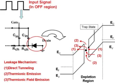
Fig. 9. Device model and cross-sectional view of (a) the TFT and (b) the gated p-i-n device.
As can be seen from Figs. 6–8, the degradation behavior of p-type poly-Si TFTs under gate ac stress in the OFF region is very similar to the case for the device under dc hot-carrier stress. Moreover, the degradation behavior of the device under gate ac stress in the OFF region is much different from that under gate dc stress. However, because the applied voltages are all in the OFF region, the device is kept in the OFF region, and there should be no channel carriers; therefore, it may not be possible for impact ionization to occur in the channel region. However, because, in the previous section, it was stated that such a behavior came from the trapped electrons on the drain side, in the case of ac stress, such a device-performance change could also be attributed to the trapped electrons. However, still, this cannot explain the reason why the degradation behaviors are so different for gate ac and dc stresses. To solve this question and to find a clearer understanding of the mechanism, a pro-posed device circuit model is shown in Fig. 9(a). Cin, Rch, and the diodes represent the gate-insulator capacitance, the channel resistance, and the source/drain junctions, respectively. The impedance between the gate and source/drain can be expressed by Z = Rch+ 1/j2πf Cin, where f represents the operation frequency. Under dc and low-frequency operations, impedance is dominated by the capacitance term, and the applied gate voltage would mainly drop across the gate insulator. For high-frequency ac operations, the capacitance term in impedance becomes smaller, and both the capacitance and resistance terms should be considered. Nevertheless, for ac operation in the OFF region, there is no induced channel formed, making the
68 IEEE TRANSACTIONS ON DEVICE AND MATERIALS RELIABILITY, VOL. 10, NO. 1, MARCH 2010
Fig. 10. Normalized gate-to-P-side-capacitance CGPcurves for the device
before and after stress.
channel resistance relatively large, and it may even become the dominant term in impedance. Back to this paper, the source and drain electrodes are grounded, and the pulse signal toggling in the OFF region is applied from the gate. The voltage drop would mainly occur across Rchand the diodes, and therefore, such a large voltage drop on the diodes in reverse bias could lead to degradation.
However, such an assumption is difficult to verify because the voltage drop in the channel can hardly be probed. Therefore, in this paper, the gated p-i-n device is adopted, where one side of the source/drain doping in fabricating the p-type TFT is changed from p+ to n− and n+. The cross-sectional view and an equivalent circuit model of the gated p-i-n device are shown in Fig. 9(b). The feature for adopting such a gated p-i-n device is that this device has the same structure to that of TFTs, while the channel voltage can be set from one side of the electrodes with forward-biased junction. Thus, this enables us to form reverse bias at one junction to simulate the condition of OFF-region gate ac stress for poly-Si TFTs. Then, by examining the capacitance curves of the TFTs and gated p-i-n devices after stress, the aforementioned mechanism can be verified.
Fig. 10 shows the normalized gate-to-P-side capacitance
CGP before and after 200-s stress. The stress condition is that the stress gate voltage, the N-side voltage, and the P-side voltage are 15, 20, and−5 V. During such a stress condition, the N-side junction is in the forward bias, while the P-side junction is in the reverse bias, and therefore, the lateral voltage difference VNP would mainly occur at the P-side junction. Referring to the figure, the CGP curves after stress show the apparent increase for the gate voltage in the OFF region, and this increase is the same for different measurement frequencies, which is just similar to the curves for the gate-ac-stressed TFTs, as shown in Fig. 7(a). In addition, both Figs. 7(a) and 10 show a slight shift for the stressed device. The similarity between the CGD and CGP curves for the ac-stressed TFT and the dc-stressed gated p-i-n device indicates the validation of the proposed mechanism. On the other hand, as for the device under gate dc stress in the OFF region, the VTHand C–V curve shift could also be explained by the trapped electrons uniformly in
Fig. 11. Model illustrating the degradation mechanism for the p-type TFT during gate ac stress in the OFF region.
the gate-dielectric layer and not confined near the source and drain regions because the voltage drop would mainly occur at the capacitors in the proposed distributed circuit model.
However, so far, this still cannot explain how such a degra-dation under gate ac stress is similar to the phenomena of degradation under dc hot-carrier stress. In dc hot-carrier stress, the electrons come from the impact-ionization event, and what is the case for the gate ac stress in the OFF region? In this case, there would be no channel carriers, and from the previous discussion, the voltage drop would mainly occur at the junction. Fig. 11 shows the model to explain such a behavior. As a large reverse bias is applied on the junction, the drift current becomes the leakage current. That means that the electrons may flow through the junction and reach the channel area, which could, in turn, move to the gate-dielectric film. In addition to the usual understanding of the leakage behavior for the largely reverse-biased junction, for the poly-Si film, there would be another point to be concerned about. Because the poly-Si film is composed of many grains and the grain boundaries would essentially form the trapping states in the bandgap, the leakage-current behavior would be enhanced because of the existence of grain boundaries near the junction. As shown in the figure, the electrons could move to the conduction band with the help of the trap state. Three possible mechanisms, i.e., direct tunneling, thermionic emission, and thermionic field emission, could occur in the depletion region [20]. As in the case of OFF-region gate ac stress, the junctions could largely be reversed biased, and the electrons could flow from the source and drain junction to the channel region, while the holes could flow out-ward. For these electrons, as they enter the channel region, they could be attracted by the applied gate voltage and then move toward the gate dielectric and eventually get trapped inside. Therefore, both on the source and drain regions, there could be electrons get trapped in the gate-dielectric layer, and this would effectively induce holes in the following measurement. This would result in altered band-diagram distribution, increased mobility, and shifted VTH, which is just the case of the channel-shortening effect under dc hot-carrier stress described in the previous section. In other words, the reliability behaviors under
TAI et al.: CHARACTERIZATION OF THE CHANNEL-SHORTENING EFFECT ON P-TYPE POLY-Si TFTs 69
gate ac stress in the OFF region and dc hot-carrier stress should all be attributed to the trapped electrons in the gate insulator near the junctions. The finding of the degradation behavior and mechanism for the device under these two operation conditions, as well as the device circuit model for poly-Si TFTs, could help designers to design poly-Si TFT circuits with higher performance and better reliability behavior.
IV. CONCLUSION
In this paper, the degradation behaviors of p-type poly-Si TFTs under dc hot-carrier and gate ac stresses in the OFF region have been thoroughly investigated. For the reliability under dc hot-carrier stress, it has been discovered that the increased mobility and shifted threshold voltage are similar to the case in p-type MOSFETs, namely, the channel-shortening effect, to which the trapped electrons in the gate insulator could be attributed. However, the reduced leakage-current behavior and the increase of capacitance behavior in the OFF region have also been caused by these trapped electrons, and such behaviors have been observed only in TFTs because of the differences in the structure and leakage mechanism. For the reliability of gate ac stress in the OFF region, similar device parameter improve-ment has also been observed, and the gated p-i-n device has been adopted to verify the proposed mechanism. The electrons resulting from the leakage current at the largely reverse-biased junctions could get trapped in the gate-dielectric film and, as a result, act like that in the case of the channel-shortening effect under dc hot-carrier stress. The finding could be very useful for the design of advanced poly-Si applications and the reliability evaluation for both the devices and circuits of p-type poly-Si TFTs.
REFERENCES
[1] H. Ohshima and Y. Matsueda, “Poly-Si TFT and driver integration technology,” Electron. Commun. Jpn., Part II: Electron., vol. 77, no. 7, pp. 46–55, Jul. 2007.
[2] S. Inoue, M. Kimura, and T. Shimoda, “Analysis and classification of degradation phenomena in polycrystalline-silicon thin film transistors fab-ricated by a low-temperature process using emission light microscopy,”
Jpn. J. Appl. Phys., vol. 42, no. 3, pp. 1168–1172, Mar. 2003.
[3] S. Inoue, S. Takenaka, and T. Shimoda, “Study of degradation phenom-enon due to a combination of contamination and self-heating in poly-Si thin film transistors fabricated by a low-temperature process,” Jpn.
J. Appl. Phys., vol. 42, no. 7A, pp. 4213–4217, Jul. 2003.
[4] Y.-H. Tai, S. C. Huang, and H. L. Chiu, “Degradation of capacitance–voltage characteristics induced by self-heating effect in poly-Si TFTs,” Electrochem. Solid-State Lett., vol. 9, no. 6, pp. G208– G210, Apr. 2006.
[5] Y.-H. Tai, S.-C. Huang, C. W. Lin, and H. L. Chiu, “Degradation of the capacitance–voltage behaviors of the low-temperature polysilicon TFTs under DC stress,” J. Electrochem. Soc., vol. 154, no. 7, pp. H611–H618, May 2007.
[6] M. Yamagata, T. Satoh, and H. Tango, “Hot-carrier-induced degrada-tion under current saturadegrada-tion bias in p-channel low-temperature polycrys-talline silicon thin-film transistors,” Jpn. J. Appl. Phys., vol. 46, no. 8A, pp. 5044–5049, Aug. 2007.
[7] S. H. Han, I. S. Kang, N. K. Song, M. S. Kim, J. S. Lee, and S. K. Joo, “The reduction of the dependence of leakage current on gate bias in metal-induced laterally crystallized p-channel polycrystalline-silicon thin-film transistors by electrical stressing,” IEEE Trans. Electron Devices, vol. 54, no. 9, pp. 2546–2550, Sep. 2007.
[8] Y. Uraoka, H. Yano, T. Hatayama, and T. Fuyuki, “Hot carrier effect in low-temperature poly-Si p-ch thin-film transistors under dynamic stress,”
Jpn. J. Appl. Phys., vol. 41, no. 1A/B, pp. L13–L16, Jan. 2002.
[9] Y. Uraoka, H. Yano, T. Hatayama, and T. Fuyuki, “Comprehensive study on reliability of low-temperature poly-Si thin-film transistors under dy-namic complimentary metal–oxide semiconductor operations,” Jpn. J.
Appl. Phys., vol. 41, no. 4B, pp. 2414–2418, Apr. 2002.
[10] Y.-H. Tai, S.-C. Huang, and C.-K. Chen, “Analysis of poly-Si TFT degra-dation under gate pulse stress using the slicing model,” IEEE Electron
Device Lett., vol. 27, no. 12, pp. 981–983, Dec. 2006.
[11] Y. Uraoka, T. Hatayama, T. Fuyuki, T. Kawamura, and Y. Tsuchihashi, “Hot carrier effects in low-temperature polysilicon thin-film transistors,”
Jpn. J. Appl. Phys., vol. 40, no. 4B, pp. 2833–2836, Apr. 2001.
[12] Y. Uraoka, T. Hatayama, T. Fuyuki, T. Kawamura, and Y. Tsuchihashi, “Analysis of hot carrier effects in low temperature poly-Si TFTs using device simulator,” in Proc. IEEE Int. Conf. Microelectron. Test Struct., 2001, vol. 14, pp. 251–256.
[13] D. K. Schroder, Semiconductor Material and Device Characterization, 2nd ed. New York: Wiley, 1998, pp. 337.
[14] M. Koyanagi, A. G. Lewis, R. A. Martin, T.-Y. Huang, and J. Y. Chen, “Hot-electron-induced punchthrough (HEIP) effect in submicrometer PMOSFETs,” IEEE Trans. Electron Devices, vol. ED-34, no. 4, pp. 839– 844, Apr. 1987.
[15] E. Takeda, Y. Nakagome, H. Kume, N. Suzuki, and S. Asai, “Comparison of characteristics of n-channel and p-channel MOSFETs for VLSIs,”
IEEE Trans. Electron Devices, vol. ED-30, no. 6, pp. 675–680, Jun. 1983.
[16] M. Brox, A. Schwerin, Q. Wang, and W. Weber, “A model for the time-and bias-dependence of p-MOSFET degradation,” IEEE Trans. Electron
Devices, vol. 41, no. 7, pp. 1184–1196, Jul. 1994.
[17] T.-F. Chen, C.-F. Yeh, and J.-C. Lou, “Effects of grain boundaries on performance and hot-carrier reliability of excimer-laser annealed poly-crystalline silicon thin film transistors,” J. Appl. Phys., vol. 95, no. 10, pp. 5788–5794, May 2004.
[18] A. Schwerin, W. Hansch, and W. Weber, “The relationship between oxide charge and device degradation: A comparative study of n- and p-channel MOSFETs,” IEEE Trans. Electron Devices, vol. ED-34, no. 12, pp. 2493– 2500, Dec. 1987.
[19] C.-J. Sheu, “Compact hot-electron induced oxide trapping charge and post-stress drain current modeling for buried-channel p-type metal–oxide–semiconductor field-effect-transistors,” Jpn. J. Appl. Phys., vol. 47, no. 8, pp. 6200–6204, Aug. 2008.
[20] K. R. Olasupo and M. K. Hatalis, “Leakage current mechanism in sub-micron poly silicon thin-film transistors,” IEEE Trans. Electron Devices, vol. 43, no. 8, pp. 1218–1223, Aug. 1996.
[21] M. Hatano, H. Akimoto, and T. Sakai, “A novel self-aligned gate-overlapped LDD poly-Si TFT with high reliability and performance,” in
IEDM Tech. Dig., 1997, pp. 523–526.
[22] K. Roy, S. Mukhopadhyay, and H. Mahmoodi-Meimand, “Leak-age current mechanisms and leak“Leak-age reduction techniques in deep-submicrometer CMOS circuits,” Proc. IEEE, vol. 91, no. 2, pp. 305–327, Feb. 2003.
[23] T. Nishibe and H. Nakamura, “Value-added SOG (system-on-glass) dis-play based on LTPS technology,” in Proc. Dig. Tech. Papers 13th Int.
Workshop AM-FPD, 2006, pp. 61–64.
Ya-Hsiang Tai (M’06) received the B.S. and Ph.D.
degrees in electronic engineering from National Chiao Tung University, Taiwan, R.O.C., in 1990 and 1996, respectively.
He became a member of the Electronics Research & Service Organization, Industrial Technology Research Institute and the TFT LCD development as a Panel Designer. He joined the project of low-temperature polycrystalline silicon (LTPS) thin-film transistor (TFT) development in Prime View International in 2000. In 2001, he joined Toppoly Optoelectronics Corporation, Chunan, Taiwan, to lead the team of LTPS TFT LCD panel design. In 2003, he joined the faculty of National Chiao Tung University, Hsinchu, Taiwan, where he is currently an Associate Professor with the Department of Photonics and the Display Institute. His current research interests include TFT device physics, active matrix display panel design, and use of TFTs as sensors on a panel.
70 IEEE TRANSACTIONS ON DEVICE AND MATERIALS RELIABILITY, VOL. 10, NO. 1, MARCH 2010
Shih-Che Huang received the B.S. degree in physics
from National Sun Yat-Sen University, Kaohsiung, Taiwan, in 2003 and the M.S. degree in electroopti-cal engineering and the Ph.D. degree from National Chiao Tung University, Hsinchu, Taiwan, in 2005 and 2009, respectively.
He is currently with the Department of Photonics and the Institute of Electro-Optical Engineering, National Chiao Tung University. His current research interests include the uniformity and behaviors of TFTs in large-area active matrix displays.
Po-Ting Chen received the B.S. degree in
electro-physics and the M.S. degree from National Chiao Tung University, Hsinchu, Taiwan, in 2006 and 2009, respectively.
He is currently with the Department of Photonics and the Display Institute, National Chiao Tung University. His current research interests include the reliability of poly-Si TFTs.