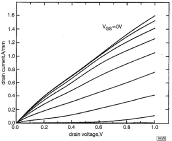
observed which results from the combination of high sheet charge density in the channel and low access resistance. The low-field source-drain resistance at V,, = OV is 0.45 Q mm. The devices dis- play a good pinchoff at V,, = -1.6V and a negligible kink effect.
1.6 1.4 E 1.2 E ?? 2 0.8 5 0.6 0.4 0.2 0.0
$
1.0 K m .- 0.0 0.2 0.4 0.6 0.8 1 .o drain voltage,V 390131Fig. 3 H E M T drain characteristics
L, = O S p , L, = 1 . 2 p , W , = 2 8 p , V,, = 0.2Vistep
A maximum DC transconductance above lS/mm is measured at VGS = 0.5V. The S-parameters of the HEMTs were measured on- wafer from 1 to 40GHz. Based on the usual 6dBioctave extrapola- tion, the device exhibits anfr andf,,, of 45 and 70GHz, respec- tively, at V,, = 0.4 and V,, = -1.1V. At this bias condition, the microwave transconductance and output conductance were 600 and 100mS/mm, respectively, and the gate leakage current was 40pA. An equivalent circuit of the HEMT was developed by fit- ting the measured S-parameters to a commonly-used circuit topol- ogy. After removal of the gate bonding pad capacitance from the equivalent circuit, an fT of 60GHz was obtained, which corre- sponds to an fTLE product of 3OGHz pn. At higher drain voltages, the effects of impact ionisation become apparent with the gate leakage current increasing and the low-frequency unilateral gain decreasing si&icantly. HEMTs with a 0 . 4 ~ gate length were also fabricated in material with a similar layer design and sheet charge density, except that a composite GaSbOnAs cap layer was employed. The overall behaviour of these HEMTs was found to be similar to those HEMTs previously described. However, they exhibited a slightly improved performance due to the shorter gate length, yielding an extrinsicf, andf,,, of 75 and lOOGHz, respec- tively, at V,, = 0.5V.
These initial results demonstrate that Si-doping in a thin I d s layer located adjacent to the AlSb barrier can be used to produce HEMTs with high sheet charge density. Optimisation of the present growth process will lead to higher sheet densities and channel mobilities. To realise the performance potential of MSb/ InAs HEMTs, the combination of this doping approach with improved buffer and barrier layer designs is needed to minimise leakage current, improve modulation efficiency, and more effec- tively manage the holes generated by impact ionisation.
Acknowledgment: This work was supported by the Office of Naval
Research. The authors thank H.B. Dietrich and C.R. Marrian for helpful discussions.
0 IEE 1998
Electronics Letters Online No: 19980219
J.B. Boos, B.R. Bennett, W. Kruppa, D. Park, M.J. Yang and B.V. Shanabrook (Naval Research Laboratory, Washington, DC 20375- 5320, USA)
E-mail: [email protected]
10 December 1997
References
BOLOGNESI, c.R., CAINE, E.J., and KROEMER, H.: ‘Improved charge control and frequency performance in AlSbiInAs-based heterostructure field-effect transistors’, IEEE Electron. Device Lett., 1994, 15, (I), pp. 16-18
BOOS, J.B., KRUPPA, w., PARK, D., BENNETT, B.R., and BASS, R.: ‘DC, small-signal, and noise characteristics of 0.1 p AlSbiInAs
HEMTs’. Proc. Ninth Int. Conf. IPRM, 1997, pp. 193-196 and KROEMER, H.: ‘High-transconductance InAsiAlSb heterojunction field-effect transistors with &doped AlSb upper barriers’, IEEE Electron. Device Lett., 1992, 13, (3), pp. 164-166 and NORMAN, A.G : ‘Remote doping of InAsiGaSb quantum wells by means of a second InAs well doped with silicon’. Inst. Phys. Conf. Ser., 1995, pp. 229-233 (no. 144)
SASA, s., YAMAMOTO, Y , IZUMIYA, s., YANO, M., IWAI, Y., and
INOUE, M.: ‘Increased electron concentration in InAsiAlGaSb heterostructures using a Si planar doped ultrathin InAs quantum well’, Jpn. J. Appl. Phys., 1997, 36, pp. 1869-1871
BENNETT, B.R., YANG, M.J., SHANABROOK, B.v., BOOS, J.B., and
PARK, D.: ‘Modulation InAs(Si) doping of InAsiAlSb quantum wells’, submitted to Appl. Phys. Lett.
WERKING, J.D., BOLOGNESI, C.R., CHANG, L-D., NGUYEN, C., HU, E.L.,
MALIK, T.A., CHUNG, S.J., STRADLING, R.A., YUEN, W.T., HARRIS, J.J.,
BOOS, J.B., KRUPPA, W., PARK, D., MOLNAR, B., BASS, R., GOLDENBERG, M., BENNETT, B.R., and MITTEREDER, J.: ‘PdiPtiAu and AuGelNiiPtiAu ohmic contacts for AlSbiInAs HEMTs’. Proc. Eighth Int. Conf. IPRM, 1996, pp. 354-357
Effects of N1,O-anneale
the short-channel e
F.C. Jong,
T.Y.
Huang, T.S. Chao, H.C. Lin,M.F.
Wang and C.Y. ChangThe authors report the effects of N,O-annealed sacrificial oxide on nMOSFETs. It is demonstrated that by adding an N,O- annealing step to the sacrificial oxide wlnch was stripped off before growing the fmal gate oxide, the reverse short-channel effects (RSCE) can still be effectively suppressed.
Introduction: Recently, the reverse short-channel effect (RSCE)
has received much attention [l - 61. Unlike the conventional nor-
mal short-channel effect (NSCE), in which the threshold voltage (V,,) decreases with decreasing channel length, RSCE involves an increase in V,, with decreasing channel length. It has now been
generally agreed that RSCE is caused by the non-uniform lateral distribution of channel surface concentration near the sourceidrain region. This lateral non-uniformity in surface dopant concentra- tion can be attributed to several processing steps, including oxida- tion-enhanced diffusion (OED), vacancy injection during source/ drain salicidation, or fluorine enhanced boron diffusion, for exam- ple. It has also been reported that by nitriding the gate dielectric (i.e. fmal gate oxide), or by performing the after-gate re-oxidation in an N,O ambient, RSCE can be suppressed [7, 81. In this Letter we report, for the frst time, that RSCE can also be effectively suppressed by performing the nitridation process on the sacrificial oxide, which is stripped off before the final gate oxide is grown.
Fabrication process and results: A typical 0.8 p, double-level-poly- silicon CMOS process was used. After LOCOS processing, the pad oxide was stripped off, and a 25nm sacrificial oxide was grown. The sacrificial oxide is usually employed in a typical MOS process flow for reducing the LOCOS-related gate oxide defect, and for improving the integrity of the fmal gate oxide by allowing the performance of the !+adjust implant and anti-punchthrough implant through the sacrificial oxide, which is then stripped off prior to growing the final gate oxide. In this study, the 25nm sac- rificial oxide in the control split was grown by a conventional dry 0, oxidation. For the N,O-annealed split, the 25nm sacrificial oxide was fxst grown by a dry 0, oxidation, followed by an N,O- annealing for 15” at 925”C, to produce a final thickness of 25nm. Wafers were then combined to receive an anti-punch- through implant (boron, 160keV, 2.5 x 1011cm-2) and a K,-adjust implant @F2, 90keV, 2.2 x 10¹²m-2) by implanting through the
sacrificial oxide. Afterwards, the sacrificial oxide was stripped off in buffered HF, and a 20 nm final gate oxide was grown in dry 0, ambient at 950°C. A polysilicon layer was subsequently deposited, POC1,-doped, and patterned to form the gate of the transistor.
I l l l l l l l l l l l l l l l l l l I
1 2 3 4 5
503111
0.80
channel length L,pm
Fig. 1 Threshold voltage ugainst channel length for control devices with conventional SiO, sacrificial oxide and devices with N20-annealed sacri- ficial oxide
+
SiO, sacrificial oxide0
N,O-annealed sacrificial oxideThreshold voltage (
vh)
against channel length for all nMOS- FETs is shown in Fig. 1. It is interesting to note that while the control devices with conventional SiO, sacrificial oxide depict RSCE (i.e.qh
increases first before finally decreasing with decreasing channel length), the devices with N,O-annealed sacrifi- cial oxide depict NSCE (i.e. V,, decreases monotonically with decreasing channel length). This result indicates that, similar to growing the final gate oxide in an N,O ambient, or performing the after-gate re-oxidation in an N,O ambient [7, 81, performing the sacrificial oxide in an N,O ambient prior to growing the final gate oxide is also effective in suppressing the oxidation-enhanced diffu- sion, resulting in a more uniform lateral surface concentration in the channel, and thereby suppressing the RSCE. To account for the observed phenomenon, it is speculated that even though the N,O-annealed sacrificial oxide was stripped off prior to growing the final gate oxide; the nitrogen which is incorporated at the Si/Si02 interface remains, serving to suppress enhanced boron diffu- sion during later processing. This is plausible because the buffered
‘0 1 2 3 4 5
0.5
channel length L,Fm 160(112/
Fig. 2 Substrate bias effects on threshold voltage against channel length for control devices with conventional SiO, sacrificial oxide and devices
with N,O-annealed sacrificial oxide A, W, SiO, sacrificial oxide
A, 0, 0 N,O-annealed sacrificial oxide
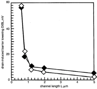
H F solution used to strip off the sacrificial oxide is known to be ineffective in etching silicon nitride. The effects of substrate bias are shown in Fig. 2. Our results confirm previous reports that RSCE subsides with the applied substrate bias [9]. Since substrate bias modulates the depletion width of the sourceidrain junction, RSCE diminishes with increasing substrate bias. The correspond- ing drain-induced barrier lowering (DIBL) effects are shown in Fig. 3. Devices with N20-treated sacrificial oxide indeed depict slightly larger DIBL, consistent with the observed NSCE in these devices (i.e. more severe K:,-lowering, compared to devices which depict RSCE).
channel length L,pm
”131
Fig. 3 Drain induced barrier lowering against channel length for control
devices with conventional S i 0 2 sacrificial oxide and devices with N,O- annealed sacrificial oxide
SiOz sacrificial oxide
0 N,O-annealed sacrificial oxide
Conclusion: We have reported, for the first time, that RSCE can
be effectively suppressed by employing an N,O-annealed sacrificial oxide. Even though the sacrificial oxide is stripped off before growing the final gate oxide, our data indicate that the incorpo- rated nitrogen at the SiiSiO, interface remains and acts to suppress enhanced boron diffusion during subsequent thermal processing. Our results suggest that the growth condition of sacrificial oxide can also affect the short-channel effects of the resultant sub- micron transistors, and should therefore be carefully considered in desigining the transistor process flow.
Acknowledgments: The authors would like to thank National Nan0 Device Laboratories for wafer processing. This work was partly supported by the Republic of China’s National Science Council through contract #NSC87-2215-E009-057.
0 IEE 1998
Electronics Letters Online no: 19980207
F.C. Jong, T.Y. Huang, M.F. Wang and C.Y. Chang (Department of Electronic Engineering, National Chiao Tung University, Hsinchu, Taiwan, Republic of China)
T.S. Chao and H.C. Lin (National Nano Device Laboratories, Hsinchu, Taiwan, Republic of China)
T.Y. Huang: also with National Nano Device Laboratories, Hsinchu, Taiwan, Republic of China
24 November 1997
References
1 MAZURE, c., and ORLOWSKI, M.: ‘Guidelines for reverse short- channel behavior’, IEEE Electron Device Lett., 1989, EDL-IO, pp.
5 5 L 5 5 8
2 ORLOWSKI, M., MAZURE, c., and LAU, F.: ‘Submicron short channel effects due to gate reoxidation induced lateral institutional diffusion’. IEDM Tech. Dig., 1987, pp. 632-635
3 HANAFI, H., NOBLE, w., BASS, R., VARAHRAMYAN, K., LI, Y., and
DALLY, A.: ‘A model for anomalous short-channel behavior in submicron MOSEET’s’, IEEE Electron Device Lett., 1993, 12, pp.
575-517
4 JACOBS, H., SCHWERRIN, A., SCHARFETTER, D., and LAU, D.: ‘MOSFET reverse short channel effect due to silicon intersitial
capture in gate oxide’. IEDM Tech. Dig., 1993, pp. 307-310 LU, c , and SUNG, J.: ‘Reverse short-channel effects on threshold
voltage in submicrometer salicide devices’, IEEE Electron Device Lett., 1989, EDL-10, pp. 446448
CHANG, c., LIN, c . , CHOU, J., HSU, c . , PAN, H., and KO, J.: ‘Anomalous reverse short-channel effect in p+ polysilicon gated p-channel MOSFET’, IEEE Electron Device Lett., 1994, 15, pp. 437439
7 TSUI, P., TSENG, H., ORLOWSKI, M., SUN, s., TOBIN, P., REID, K., and TAYLOR, w.: ‘Suppression of MOSFET reverse short channel effect by N,O gate poly reoxidation process’, IEDM Tech. Dig., 1994, pp. 501-504
combination effects of nitrogen implantation at SID extension and
N 2 0 gate oxide on 0.18pm nMOSFET’. Int. Symp. on VLSI-TSA,
1997, pp. 316-320
9 ARORA, N., and SHARMA, M.: ‘Modeling the anomalous threshold voltage behavior of submicron MOSFET’s’, IEEE Electron. Device Lett., 1992, 13, pp. 92-94
5
6
8 CHAO, T., CHIEN,, LIN, H., CHEN, L., HUANG, T., and CHANG, C.: ‘The
GalnP/AllnP tunnel junction for GalnP/GaAs
tandem solar cells
W. Li, J. Lammasniemi, A.B. Kazantsev, R. Jaakkola,
T. Makela and M. Pessa
A GaInP/AlInP tunnel diode has been grown by a gas-source molecular beam epitaxy method. A high conductance of 1 5 M cm2 at 2.7mV has been achieved. Using closely optimised growth
conditions, very high carrier concentrations, both in GaInP and AlInP, have been obtained.
A GaInPiGaAs tandem solar cell consisting of a thin GaInP top cell and a GaAs bottom cell has a si@icantly higher conversion efficiency than conventional single-junction solar cells [l]. One of the critical issues in the growth of such a two-terminal monolithic tandem cell is a tunnel junction for the inter-cell connection. The tunnelling interconnect must not only pass the device current with minimal electrical loss but also transmit the appropriate portion of the optical spectrum to the underlying subcell. The GaInP/AlInP tunnel junction may provide the desired interconnect. It tends to increase the quantum efficiency of the bottom cell by eliminating the absorption loss typical of the GaAs tunnel layer [l]. Con- versely, the p+-n+ GaInP junction is difficult to prepare for exam-
ple by metal organic chemical vapour deposition (MOCVD), which is the most commonly used method for the growth of solar cells, because of the rapid diffusion of p-type dopants (Zn).
20
10 I I a I * I . , .
T°C m
Fig. 1 Net carrier concentrations in ANnP and GaInP layers grown by
GSMBE against Be and Si oven temperatures
0 AlInP: Be
A
GaInP: Be W A1InP: Si 0 Ga1nPi:SiRecently, we have shown that it is possible to prepare GaInP/ GaAs tandem cells by means of gas source molecular beam
epitaxy (GSMBE) [2]. Compared to MOCVD, GSMBE yields a higher p-type doping efficiency and less severe diffusion of the p-
type dopant (Be). In this Letter, we present a p+-n+ GaInP/AlInP tunnel diode grown by GSMBE. In GSMBE, elemental solid sources are used to produce the group-I11 beam fluxes, while As, and P, are produced from cracked ASH, and PH,. The growth temperature inour experiments was -500°C.
Fig. 1 shows the net carrier concentrations in Si and Be-doped GaInP and AlInP, as deduced from Hall-effect measurements. The doping characteristics of AlInP differ significantly from those of GaInP. Doping with Si resulted in the m a x i ” electron concen- tration of 1.8 x 10’9m-3 in GaInP and 5.3 x 101*cm3 in AlInP. A further increase in Si concentration caused a decrease in carrier concentration, due to the amphoteric nature of Si. Doping with Be yielded the m a x i ” hole concentration of 3.7 x 1019cm3 for GaInP and 4.7 x lO’*~m-~ for AlInP. The hole concentrations are limited by a non-homogeneous redistribution of Be in the doped layer [3]. The above-mentioned doping levels are among the high- est obtained to date by any growth method.
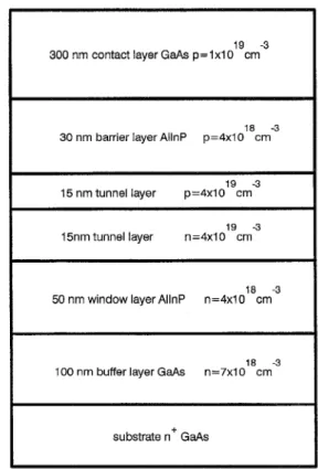
19 -3 300 nm contact layer GaAs p=lxlO cm
30 nm barrier layer AllnP p=4x10 cm
I
I
19 -3I
15 nm tunnel layer p=4x10 cmI
19 -3 15nm tunnel layer n=4x10 cm50 nm window layer AllnP n=4x10 cm
-3
I
18 -3
100 nm buffer layer GaAs n=7x10 cm
substrate nf GaAs
m Fig. 2 Schematic structure of GaInP/AlInP tunnel diode
voltage, mV
Fig. 3 I- V characteristics of GaInP/AlInP tunnel diode
The schematic structure of a GaInP/AlInP tunnel diode suitable for use in a GaInP/GaAs tandem cell is shown in Fig. 2. We have made the GaInP and AlInP layers lattice-matched to a GaAs:Si (001) substrate within a range of accuracy from A d a = - 600 to
200ppm. The diodes were fabricated by alloying TilPUAu contacts to the p+ GaAs layer and etching photolithographically defmed