Electrical and dielectric properties of (Ba
0
.5
Sr
0
.5
)TiO
3
thin films prepared
by a hydroxide–alkoxide precursor-based sol–gel method
M. Nayak, S.Y. Lee, Tseung-Yuen Tseng
∗Department of Electronics Engineering and Institute of Electronics, National Chiao Tung University, 1001 Ta Hsueh Road, Hsinchu 300, Taiwan, ROC
Received 6 February 2001; received in revised form 28 June 2001; accepted 20 August 2001
Abstract
Thin films of barium strontium titanate with composition (Ba0.5Sr0.5)TiO3were prepared by a sol–gel method using Ba-, Sr-hydroxides, titanium(IV) isopropoxide as source materials and 2-methoxyethanol as the solvent. Well-crystallised films were obtained at relatively low temperatures. We observed grain growth accompanied with increase in the dielectric constant as the annealing temperature increased. The films prepared from this method and annealed at 800◦C showed high dielectric constant of 650. Typical leakage current density of the film annealed at 700◦C is 0.8 × 10⁻⁶at 75 kV cm–1. The change in electrical characteristics of the films has been correlated to their microstructure, which revealed that the concentration change affected the film porosity and grain size distribution. The results indicate that the microstructure could be tailored by changing the precursor solution concentration.
© 2002 Elsevier Science B.V. All rights reserved.
Keywords: Sol–gel; Thin film; Barium strontium titanate; Electrical properties; Dielectric properties
1. Introduction
Thin films of high dielectric constant materials such as barium strontium titanate (BST) have been widely inves-tigated for their feasibility in thin film integrated storage capacitors in giga bit dynamic random access memory (DRAM). This is mainly due to their high dielectric constant, low dielectric loss, low leakage current, low-temperature coefficient of dielectric constant and the composition de-pendent Curie temperature. In the DRAM operating tem-perature BST should be in paraelectric form to avoid fatigue and ageing due to the ferroelectric domain switching [1–6]. In addition to the DRAM applications BST thin films have been identified for a variety of other applications [7–12]. Each application has its own material property requirement. Interestingly, BST thin films can be used in a variety of applications because of their composition-dependent proper-ties. Simply by changing Ba/Sr ratio and also by doping iso-valent or alioiso-valent dopants, properties can be modified to fit into a given application. However, whether or not BST thin films can be successfully applied largely depends on more thorough understanding the material’s properties. The depo-sition techniques and electrical properties of BST films have received increasing interest [12–15]. According to those investigations, the electrical and dielectric properties and
re-∗Corresponding author. Fax:+886-35-724-361. E-mail address: [email protected] (T.-Y. Tseng).
liability of BST films depend heavily upon the composition, thin film deposition method and post-deposition process-ing, base electrodes, microstructure, film thickness, surface roughness, oxygen content and homogeneity of the film [4]. BST thin films have been prepared by variety of meth-ods [15–21]. Among these methmeth-ods, sol–gel processing offers some advantages over other methods in terms of low-temperature preparation, compositional homogeneity, ability to coat large area and complex-shaped substrates, purity (because of the liquid form of precursors which can be easily purified by distillation), cost effective and simple. In the present study, we investigated the electrical and di-electric properties of the Ba0.5Sr0.5TiO3thin films prepared
by a sol–gel method using hydroxide–alkoxide precursors. It is highly economical to use cheaper hydroxides of the Ba and Sr as the Ba- and Sr-sources instead of expensive and unstable alkoxide precursors. Not much work has been done on the sol–gel preparation of BST thin films using the hydroxide–alkoxide method and the study of their electrical and dielectric properties. Burhanuddin et al. [18] prepared Ba0.5Sr0.5TiO3 using Ba- and Sr-hydroxide as the source
of Ba and Sr by chemical solution deposition method and studied the I–V characteristics of MIS-type device which showed a diode-like character. Hayashi et al. [20] prepared Ba0.7Sr0.3TiO3thin films by sol–gel method using
hydrox-ides as the Ba-, Sr-source and methanol as the solvent. How-ever, in both studies detailed investigation of electrical and dielectric properties has not been carried out.
0254-0584/02/$ – see front matter © 2002 Elsevier Science B.V. All rights reserved. PII: S 0 2 5 4 - 0 5 8 4 ( 0 1 ) 0 0 5 6 6 - 1
2. Experimental details
The Ba0.5Sr0.5TiO3 thin films were prepared following
a procedure similar to Burhanuddin’s method [18]. Multi-component BST precursor solution was prepared using high purity Ba(OH)2·8H2O, Sr(OH)2·8H2O and titanium(IV)
isopropoxide (Ti(OC3H7)4) as the starting materials and
2-methoxy ethanol as the solvent. The required amounts of Ba-, Sr-hydroxides were separately mixed in 2-methoxy
ethanol and refluxed at 120◦C for 3–4 h. Extensive
re-fluxing is very essential to evaporate the water present in each solution from the source materials and also for the completion of the complexation reaction between starting material and the solvent to form complex sol. Similarly, stoichiometric amount of Ti-isopropoxide was mixed with
2-methoxy ethanol separately and refluxed at 120◦C for
3 h. These three solutions after cooling to room temperature
were then mixed and refluxed at 120◦C for 3 h to form a
homogeneous mixture of BST-precursor and concentrated by solvent evaporation which forms the stock solution. Thin films were prepared by spin coating using this stock solution after appropriate dilution (0.28, 0.15, 0.08 M) us-ing 2-methoxy ethanol. The solution was syrus-inged through 0.2m filter on to Pt/SiO2/Si, Pt/Ti/SiO2/Si substrates and
spin coated at 5000 rpm for 30 s. As deposited films were then dried in an oven at 140◦C for solvent evaporation for
10 min and then pyrolysed at 500◦C for 30 min. Films of
thickness 150–650 nm were deposited by repeating the spin coating–solvent evaporation–pyrolysis steps several times (10–50 layers). After obtaining the films of sufficient thick-ness the films were post-annealed at different temperatures
in the range 500–800◦C. The substrates were prepared by
depositing 1000 Å Pt by d.c. sputtering over a 1000 Å Ti buffer layer on a Si-wafer with 932 Å thermal SiO2barrier
layer.
The crystallinity of the films was probed by X-ray
diffraction (XRD, Shimadzu XD-5) using Ni-filtered Cu K␣
radiation source. Film thickness and microstructure were characterised by Hitachi S4700 scanning electron micro-scope (SEM). High resolution X-ray photoelectron spec-troscopy (XPS) was performed using Physical Electronics ESCA PHI 1600. The XPS system was equipped with Al/Mg dual anode and multichannel detector. The system operated at a base pressure of 5× 10⁻¹⁰Torr. For the electrical char-acterisation, a metal–insulator–metal (MIM) type of struc-ture was formed by depositing 50 nm thick top Pt electrode
with diameters of 150, 250 and 350m by d.c. sputtering
through a shadow mask. The capacitance–voltage (C–V) characteristics were measured by using Hewlett-Packard (HP) HP4194A impedance/gain phase analyser at 100 kHz as a function of sweeping voltage from positive to nega-tive voltage d.c.-bias. Dielectric constant of the films was calculated using the measured capacitance, thickness and electrode area. The current–voltage (I–V) measurements were performed by using HP4156A under both negative and positive voltage sweeps.
3. Results and discussion
3.1. Thin film deposition
The stabilisation of the precursor solution was a diffi-cult step during the preparation of BST films because of the molecular water associated with Ba- and Sr-hydroxides released to the solvent during the refluxing step resulted in preferential precipitation of the Ti by rigorous hydrolysis. This problem was overcome by individually reacting the starting materials with 2-methoxy ethanol and evaporating the water content in the Ba- and Sr-solution by refluxing for 3–4 h before mixing to form BST complex sol. The so-lution once stabilised can be stored for months without any precipitation. The individual precursor solution obtained by reacting the Ba-, Sr-hydroxides and Ti-isopropoxide with 2-methoxy ethanol were filtered and analysed by static gravimetry (by solvent evaporation of a small quantity of the solution and decomposing the resultant precursor at 700◦C) prior to mixing them together to confirm the composition of the solution.
The BST film deposited on the Si/SiO2/Pt substrate peeled
off very often on pyrolysis at the interface between bottom Pt-electrode and the Si/SiO2substrate. This is mainly due to
the poor adhesion of Pt-thin film on the Si/SiO2 substrate.
The adhesion of bottom Pt-electrode on the Si/SiO2substrate
was greatly improved by depositing a 100 nm Ti buffer layer between Si/SiO2and Pt layer. However, Ti buffer layer
incor-poration lead to added complexities by way of Ti-migration onto the surface of bottom Pt-electrode on annealing.
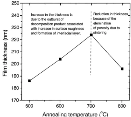
Fig. 1 shows the thickness variation of the 500◦C pyrol-ysed thin film as a function of annealing temperature de-termined from the SEM cross-sectional image. The thick-ness of the sample increased initially up to an annealing
temperature of 700◦C and thereafter showed a decrease.
Fig. 1. Variation of the thickness of the 500◦C pyrolysed film after annealing at different temperatures determined using SEM cross-sectional image.
Thickness increased from 186 nm for 500◦C annealed sam-ple to 224 nm at 700◦C and decreased to 196 nm after an-nealing at 800◦C. The initial increase in the thickness is due to two reasons. First reason is, swelling or increase in surface roughness due to the escape of embedded pyrol-ysed decomposition products from the film and the second reason is due to the formation of an additional interfacial layer on the surface of bottom Pt-electrode by Ti-migration through the grain boundaries and on the surface which
re-acts with oxygen to form TiOx [21–23]. This additional
ill-defined interfacial layer contributes to the film thickness. Ti-migration rate and formation of interfacial layer are very marginal at lower temperatures but is very severe as the annealing temperature is increased because of the fact that Ti-diffusion is activated process. Hence, the contribution to film thickness from this layer at lower temperature such as 500◦C is negligible. As the annealing temperature in-creased, the interfacial layer grows in thickness contribut-ing more and more to the film thickness. The decrease in the thickness of the film annealed above 700◦C is due to the fact that, above this temperature the film is free of de-composition products and sintering process dominates to form denser film by way of grain growth and eliminating porosity. Thus, over all thickness is reduced compared to the film annealed at 700◦C but thickness is higher than the sample annealed at 500◦C because of the contribution from the interfacial layer formed by annealing the film at higher temperatures.
Formation of interfacial layer of TiOx on top of
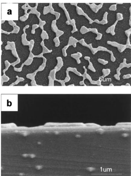
bot-tom Pt-electrode after annealing at higher temperatures was further confirmed by SEM and X-ray photoelectron spec-troscopy (XPS). Fig. 2 shows the surface and cross-sectional image of 800◦C per 2 h annealed Pt/Ti/SiO2/Si wafer.
Sur-face image shows the formation of random islands on the Pt surface due to the Ti-migration. The cross-sectional image shows that the thickness of each island is around 128 nm, which contributes to BST film thickness. The composition of this surface discontinuous layer has been determined us-ing XPS. Fig. 3 shows the strong line spectra of the surface of Pt/Ti/SiO2/Si wafer after annealing at 500 and 800◦C,
respectively. The surface analysis of the wafer annealed at 500◦C did not show any XPS signal (Fig. 3a) related to the Ti or oxygen. Only signal detected is of Pt. However, the
same wafer after annealing at 800◦C per 2 h showed
sig-nals corresponding to Ti and oxygen along with that of Pt (Fig. 3b). The XPS results confirm the formation of interfa-cial TiOx layer on the surface of bottom Pt-electrode after annealing at higher temperatures such as 800◦C.
3.2. Phase formation characteristics
X-ray diffraction study of the films post-annealed at differ-ent temperatures indicated that reasonably well-crystallised films were obtained at a temperature as low as 500◦C. The XRD pattern showed all major X-ray reflection peaks of perovskite BST phase indicating the polycrystalline nature
Fig. 2. SEM (a) surface and (b) cross-sectional image of Pt/Ti/SiO2/Si
wafer after annealing at 800◦C for 2 h showing the TiOx islands on the surface of Pt film formed by the migration of Ti through the Pt-grain boundaries. The thickness of the interfacial layer formed is about 128 nm.
of the film with (1 1 0) as the major peak. Crystallinity of the thin films improved with increase in the annealing tem-perature, indicated by the increase in intensity of the X-ray diffraction peaks. The average grain size was calculated by using the full width at half maximum of the dominant (1 1 0)
peak using Scherrer’s equation [24]. The 500◦C annealed
sample showed an average grain size of 20 nm, which in-creased to 32 nm on annealing above 600◦C. The grain size of the films increased with increasing annealing tempera-ture. Increase in grain size with increasing annealing tem-perature is expected because of the sintering wherein the small grains coalesce to form larger grains. Lattice param-eter of the thin films annealed in the temperature range
500–700◦C remained almost constant (Table 1). However,
when annealed at temperatures above 700◦C, a small
de-crease is observed. Film annealed at 800◦C showed 0.02 Å contraction in lattice parameter with respect to the film an-nealed at 500◦C. This type of lattice shrinkage was also
observed in sputtered BaTiO3and BST, which has been
at-tributed to non-equilibrium and highly distorted states within the films [25]. This indicates that the low-temperature an-nealed films are in more strained form and the atomic enti-ties must have been in the non-equilibrium positions which relaxes to the equilibrium position when annealed at higher temperatures, hence a contraction in lattice parameter is obvious.
Fig. 3. XPS strong line spectra of Pt/Ti/SiO2/Si wafer after annealing at: (a) 500◦C and (b) 800◦C for 2 h.
Similarly, XRD patterns were obtained for the films pre-pared from different concentration solutions (0.08, 0.15 and 0.28 M) on to platinised Si-wafer, which showed phase pure BST thin films. The average grain size calculated using Scherrer’s equation was approximately 32 nm.
Table 1
Lattice parameter after annealing the thin film at different temperatures calculated using (1 1 0) reflection and Pt (1 1 1) peak as the standard Annealing temperature (◦C) Lattice parameter (Å)
500 3.9421
600 3.9399
700 3.9389
800 3.9217
3.3. Microstructural analysis
The SEM surface micrographs of the films annealed at
500 and 600◦C showed crack-free uniform and smooth
mi-crostructure composed of ultrafine grains (<10 nm).
How-ever, the micrograph of the 600◦C annealed film showed
slightly larger grain size than the 500◦C annealed film along with some locally crystallised sites with higher grain size, which acted as the nucleation sites for further grain growth as the annealing temperature increased. These preferential nucleation centres might be originating from the TiOx is-lands formed on the bottom electrode at this temperature. Further increase in annealing temperature resulted in spread-ing of these nucleation sites and the surface image of 700◦C
annealed sample shows uniform spherical grains of 40– 70 nm size along with nanosized porosity formed because of the growth of ultrafine grains formed at low temperatures and also due to the escape of carbonatious decomposition products trapped in the film. Annealing of the sample at 800◦C further increased the grain size and the majority of the pores are eliminated by sintering of the film at this tem-perature. Also, the surface roughness has increased mani-folds and the grain size distribution is large ranging from 25 to 100 nm. This type of wider-sized grain distribution reduces the film porosity. SEM analysis of the samples an-nealed at various temperatures revealed an increase in grain size with the increase in annealing temperature.
The SEM micrographs of the films prepared using three different concentration precursor solutions and annealed
at 700◦C, showed varied microstructure with change in
concentration. Film prepared from 0.08 M solution showed more spherical and platy grains of size 40–70 nm, whereas 0.15 M solution derived film showed agglomerated spheri-cal grains in the same size range and that of 0.28 M solution shows more platy elongated grains. The remarkable dif-ference between these films is in the grain morphology, extent of agglomeration and the porosity. Film prepared from 0.08 M precursor solution is less porous and the film prepared from 0.28 M solution is highly porous with ag-glomerated grains. Results indicate that, the porosity in the film increases with increase in precursor solution concen-tration. The lower porosity in the film deposited using dilute solution is due to the fact that individual layers are thin and hence will be thermally cycled more times which results in effective pyrolysing of the organics than film prepared from the concentrated solution. In sol–gel preparation, the individual layer on pyrolysis leaves behind pores in the film, which will be covered by subsequent layers. More the number of layers the pore density will be lower. Also, the individual layers of the films prepared from the con-centrated solution are thicker than the film prepared from dilute solution, hence require less number of layers to at-tain required thickness and incorporates more carbonatious decomposition products in the film. On annealing at 700◦C these embedded impurities burn-off leaving behind pores in the film and in the process changes the microstructure.
3.4. Leakage current characteristics
The leakage current density vs. electric field (J–E) plot of the BST thin films annealed at different temperatures is shown in Fig. 4, which shows variation with anneal-ing temperature. In the positive voltage region of J–E plot, film annealed at 500◦C shows larger leakage current than that annealed at higher temperatures. Lowest leakage cur-rent (10−6A cm−2in the electric field range<100 kV cm–1)
is observed for the film annealed at 600 and 700◦C. The
800◦C annealed film shows slightly higher leakage current than 600 and 700◦C annealed films but is lower than 500◦C annealed film. The J–E characteristics of all the samples
Fig. 4. J–E plot of BST thin films post-annealed at different temperatures for 2 h in air.
show three different regions indicating the contribution from three different types of conduction mechanisms at low, in-termediate and high field regions. At lower voltage the film
shows ohmic behaviour(J ∝ E) and deviates at
intermedi-ate and higher fields. The turn-on electric field from ohmic to non-ohmic region decreased as the annealing temperature increased. The turn-on electric field for the sample annealed at 500 and 600◦C is around 300 kV cm–1and that of film annealed at 700 and 800◦C is around 200 and 150 kV cm–1, respectively.
The leakage current characteristics of the thin film capac-itor depends upon several factors such as the top and bot-tom electrode interface, surface roughness, the integrity of the electrodes, formation of interfacial low impedance layer or presence of any impurity second phase in the dielec-tric film which provides an easy path for electrons which can dramatically increase the leakage current. Formation of hillocks on the bottom Pt-electrode due to repeated thermal cycling is another reason for the increased leakage current in sol–gel derived films. High leakage current observed in
the case of 500◦C annealed samples might be due to the
presence of embedded pyrolysed decomposition products in the film. The decrease in the leakage current with increase in annealing temperature is because of the burn-off of these embedded decomposition products. Increase in leakage cur-rent for the film annealed at 800◦C is due to the increase in the grain size, as observed by SEM analysis, which con-tributes to surface roughness. The grain size of the film could play an important role in deciding the surface roughness; the small grain size films usually have smooth surface and low leakage current. SEM surface analysis of the 500 and 600◦C annealed samples show smooth fine grain surface, of which a low leakage current is expected. But the experimen-tal result of 500◦C annealed film is contrary, which shows higher leakage current indicating the presence of embedded
decomposition products. On annealing above 600◦C these decomposition products are completely burnt-off and the film is in the more pure form than the 500◦C annealed film and show the lowest leakage current. On further increas-ing the annealincreas-ing temperature, the film sinters resultincreas-ing in higher grain size associated with higher roughness. Hence, a higher leakage current is expected from the film annealed at 800◦C than the 700◦C annealed film as observed experi-mentally. The surface roughness of the film is also affected by incorporation of a bottom adhesive layer such as Ti. The Ti-migration onto the surface of the bottom Pt-electrode makes the surface rough by forming islands as shown in Fig. 2. This will increase the roughness of the film and also increases the leakage current.
The grain size effect on the leakage current characteris-tics is more prominently reflected in the turn-on voltage. It is reported that in BST films turn-on voltage increases as the grain size decreases [15]. The films with smaller grain size similar to the films annealed at 500 and 600◦C is expected to show higher turn-on voltage and as the grain size increases the turn-on voltage is also expected to shift to the lower voltages. The smaller grain size produces more grain bound-aries which are highly resistive, hence requires higher field to achieve turn-on from ohmic to non-ohmic region [15].
The leakage current characteristics are distinctly different in the positive and negative voltage region. The J–E char-acteristic of MIM-type device is expected to be symmetric. However, Fig. 4 shows that J–E characteristics are not sym-metric. In the negative voltage region, maximum leakage current is observed for the sample annealed at 800◦C and
minimum is for the 500◦C annealed sample. The turn-on
voltage for the 600, 700 and 800◦C annealed samples is as
low as 50 kV cm–1 and that of 500◦C annealed sample is
250 kV cm–1.
The asymmetry in positive and negative voltage part of the J–E characteristics is normally brought in due to the dif-ference in the top and bottom electrode work functions, the difference in two interfaces and also implies that the leakage current is electrode-limited [17]. It is generally known that the leakage current of Pt/BST/Pt is controlled by Schottky barrier at the BST/electrode interface in which the leakage current is controlled by Schottky barrier heights at the top BST/electrode and bottom BST/electrode interface [26,27]. If these potential barriers are not identical, then the J–E char-acteristics would not be symmetric. In the present case, the reason for the asymmetry in the J–E characteristics is due to the difference in the top and bottom electrode interfaces. The difference in interface is brought about by Ti-migration to the surface of the bottom Pt-electrode as already discussed in the previous sections. It is also proved from XPS results that on migration to the surface, Ti reacts with ambient oxy-gen to form TiOxinterfacial layer effectively modifying the bottom electrode interface. The effect of Ti-diffusion on bot-tom electrode also depends upon annealing temperature. At lower temperatures, the Ti-diffusion rate is very slow, be-cause the diffusion is an activated process which derives the
activation energy from the heat energy. XPS results proved that the film annealed at 500◦C did not have Ti on the sur-face. As the annealing temperature increases the diffusion rate also increases and more and more Ti migrates to the sur-face of Pt through grain boundaries and reacts with oxygen
to form TiOx [21–23] as also proved by XPS results. This
reaction is more severe at temperatures higher than 600◦C. At 800◦C, all Ti must have been diffused to the surface and
formed TiOx islands as shown in the SEM image of the
wafer annealed in air at 800◦C for 2 h in Fig. 2. This implies that each temperature-annealed sample will have a differ-ent bottom electrode interface effectively changing the J–E characteristics of the thin films annealed at different tem-peratures. The minimum leakage current (positive voltage region) in the case of 600–700◦C annealed film indicates ideal interfacial characteristics for this sample.
The leakage current of the samples prepared by the present method is comparable to that reported in literature for thin films of Ba0.7Sr0.3TiO3prepared by using acetate precursors
and spin coated on Pt/Ti/SiO2/Si substrate [19]. The 600◦C
annealed sample in the present study at 75 kV cm−1showed leakage current of 0.8 × 10⁻⁶A cm−2, in comparison to the reported value for the film prepared from acetate precursors 0.17 × 10⁻⁶A cm−2[19]. However, the solution concentra-tion, deposition conditions and post-deposition processing differed.
3.5. Effect of concentration on the J–E characteristics
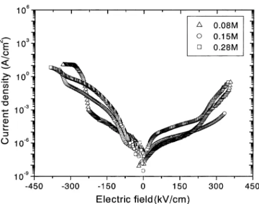
Concentration of the BST precursor solution showed pro-nounced influence on the leakage current behaviour of the thin films as it decides the microstructure of the film at a given annealing temperature. BST films for this study were prepared using different concentration solutions (0.08, 0.15, 0.28 M) and remaining conditions such as solvent evapo-ration (140◦C), pyrolysis (500◦C), annealing temperature (700◦C) and duration of these processes were fixed. Fig. 5 shows the J–E characteristics of the BST thin films pre-pared using solutions of three different concentrations and annealed at 700◦C for 2 h. The J–E plot for thin films de-posited using each concentration is different. Important ob-servations are:
1. Leakage current density increased with increase in pre-cursor solution concentration. Leakage current density of the BST film prepared from 0.28 M solution is larger than those prepared from the low concentration solution. 2. The turn-on voltage is different for the film deposited
from different concentration solution: film prepared from high concentration solution (0.28 M) showed turn-on voltage of approximately 250 kV cm–1, that of film
pre-pared from 0.15 and 0.08 M solution is 200 kV cm–1in
the positive voltage region.
3. The positive and negative field J–E behaviour is different and asymmetric for the reason already described in the previous section.
Fig. 5. J–E plot of BST thin films prepared from precursor solutions of three different concentrations and post-annealed at 700◦C per 2 h in air.
The difference in the leakage current behaviour of the films prepared from different concentration solutions is because of the difference in microstructure. The microstruc-ture of the films prepared from different concentration solutions showed distinct difference in terms of porosity, surface roughness, grain size and morphology.
3.6. Dielectric properties
Fig. 6a and b shows the variation of dielectric constant and the loss tangent with applied d.c.-electric field of the BST thin films annealed at different temperatures. With the increase in the annealing temperature the dielectric constant also increased. The 800◦C annealed thin film shows maxi-mum dielectric constant of around 650 and that of the film annealed at 500◦C is the lowest, approximately 325 at zero bias. The electric field at which the dielectric constant has its maximum value is not located at the zero bias field in-stead shifted towards the positive voltage region. Maximum dielectric constant field (Em) has shifted consistently from
43 kV cm–1for 500◦C annealed film to 20 kV cm–1for the film annealed at 800◦C.
The increase in dielectric constant with increasing an-nealing temperature is attributed to the increase in the grain size and crystallinity of the thin film. XRD and SEM results showed that with annealing temperature, crystallinity and grain size increased, which in turn resulted in larger polari-sation density there by increasing the dielectric constant. It is well known that as the grain size increases the dielectric constant increases and as the porosity in the film increases, the dielectric constant decreases.
The shift in electric field at which the dielectric constant has its maximum is because of the same reason that change in the interface characteristics brought in by annealing the film at different temperature and associated Ti-migration problem
Fig. 6. (a) Variation of the 100 kHz dielectric constant with applied electric field for the BST thin films annealed at different temperatures for 2 h in air and (b) Variation of the loss tangent with applied electric field for the BST thin films annealed at different temperatures for 2 h in air.
which modifies the interface. The space charge capacitance at the two interfaces is different because of the difference in interface characteristics.
The dielectric loss is maximum for film annealed at 500◦C (0.14 at zero bias). Lowest loss tangent is observed for the
BST films annealed at 600 and 700◦C (0.04). Also, these
thin films show approximately similar behaviour under the bias field variation. Further increase in the annealing tem-perature to 800◦C resulted in the increase of loss tangent to higher value (∼0.06 at zero bias) than the film annealed at 600 per 700◦C but much lower than the film annealed at 500◦C.
The dielectric loss originates from two mechanisms: re-sistive loss and relaxation loss [15]. Rere-sistive loss mecha-nism involves energy consumption by the mobile charges in the film; whereas, in the case of relaxation loss mechanism, it is relaxation of the dipole which dissipates the energy. If
there is very few mobile charges in the film then the later mechanism is dominating. The resistive loss mechanism is directly connected to the leakage current of the film: if the leakage current is higher the loss is also higher. Alterna-tively, if the dielectric constant of the film is larger, then an increase in the dielectric loss is obvious due to the contri-bution from the second mechanism. Enhanced polarisation increases the energy dissipation during the relaxation. The higher dielectric loss of 500◦C annealed film is due to the higher leakage current of the film. Lowest leakage current is observed for the films annealed at 600 and 700◦C, hence a low dielectric loss. The increase in the loss tangent after annealing at 800◦C is due to the increased leakage current and also due to dipole relaxational loss because of the en-hanced polarisation effect.
3.7. Effect of concentration on the dielectric constant
The precursor solution concentration dependence of the dielectric constant is studied by depositing approximately same thickness films using different concentration precursor solutions followed by post-deposition annealing at 700◦C per 2 h. The results indicate that dielectric constant and the loss tangent varied with precursor solution concentration. Fig. 7 shows the 100 kHz dielectric constant vs. electric filed plots of the thin films prepared from precursor solutions of three different concentrations and annealed at 700◦C per 2 h. The dielectric constant of the thin film prepared from the dilute solution (0.08 M) is larger than that of films prepared from 0.15 and 0.28 M solutions. At zero bias, the dielec-tric constant of the BST film prepared from 0.08 M solution is around 550, whereas that of 0.15 and 0.28 M solution is approximately 475. The films prepared from both 0.15 and 0.28 M solutions showed almost similar variation of dielec-tric constant and loss tangent with the bias d.c.-field.
Fig. 7. Variation of the 100 kHz dielectric constant with applied electric field for the BST thin films prepared using precursor solutions of three different concentrations and annealed at 700◦C for 2 h in air.
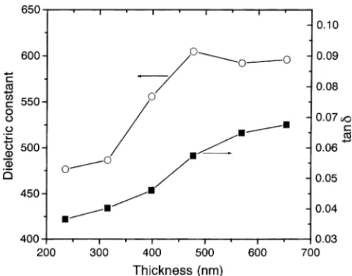
Fig. 8. Variation of 100 kHz dielectric constant and loss tangent of the BST thin film prepared from 0.28 M solution as a function of thickness.
Above results can be explained based on the microstruc-ture as determined by SEM analysis. Films prepared from three different concentration precursor solutions differed in their microstructure, in particular porosity and morphology. The film prepared from the dilute solution showed lower porosity than the films from concentrated solution. This re-duced porosity increases the polarisation density thereby in-creasing the dielectric constant of the film prepared from dilute solution.
3.8. Thickness dependence of the dielectric constant
Thickness dependence of the dielectric constant and the loss tangent of the BST thin films prepared from 0.28 M precursor solution is plotted in Fig. 8. As the thickness in-creased the dielectric constant also increases and saturates above a thickness of 500 nm. The increase in the dielectric constant with film thickness is due to the increase in grain size, film crystallinity and also the film density. In sol–gel method of preparation, as the number of layers increases the film porosity decreases because subsequent layers coated on the former pyrolysed layer covers-up the pores and bulk defects left behind by the organic burn-off. The saturation in dielectric constant above a certain thickness is due to the limitation in the grain size that can be achieved by this method of preparation. Similar to dielectric constant, loss tangent also increased with increase in film thickness. The increase in loss tangent is due to the increased dipole relax-ational loss because of the larger dipole density, which is also a reason for increased dielectric constant.
4. Conclusions
In conclusion, Ba0.5Sr0.5TiO3thin films can be deposited
on the Pt/Ti/SiO2/Si substrate at a low-temperature using
of Ba and Sr as the Ba-, Sr-sources, Ti-isopropoxide as the Ti-source and 2-methoxy ethanol as the solvent. How-ever, film prepared at 500◦C even though X-ray crystalline failed to show better electrical characteristics because of the presence of unburned embedded decomposition products. Reasonably, good film with low leakage and high dielec-tric constant can be obtained after annealing above 700◦C wherein the embedded carbonatious decomposition products must have been burnt-off. The leakage current characteristic and the dielectric constant depend on the processing param-eters such as annealing temperature, film thickness and pre-cursor concentration. Another important finding of the study is the microstructure can be tailored by changing the con-centration of the precursor solution. As a whole, our study highlights the intricate relationship between the film pro-cessing, microstructure and the properties of the film.
Acknowledgements
Support for this work by National Science Council of Tai-wan, ROC under project NSC 89-2112-E009-040 is grate-fully acknowledged.
References
[1] H. Kawano, K. Mori, Y. Nakayama, J. Appl. Phys. 73 (1993) 5141. [2] T. Horikawa, N. Mikami, T. Makita, J. Tanimura, M. Kataoka, K.
Sato, M. Nunoshita, Jpn. J. Appl. Phys. 32 (1993) 4126.
[3] H. Kawano, K. Mori, Y. Nakayama, J. Appl. Phys. 73 (1993) 5141. [4] S. Ezhilvalavan, T.Y. Tseng, Mater. Chem. Phys. 65 (2000) 227. [5] M. Yamamuka, T. Kawahara, T. Makita, A. Yuuki, K. Ono, Jpn. J.
Appl. Phys. 35 (1996) 729.
[6] K. Numata, Y. Fukuda, K. Aoki, A. Nishimura, Jpn. J. Appl. Phys. 34 (1995) 5245.
[7] W. Zhu, O.K. Tan, J. Deng, J.T. Oh, J. Mater. Res. 15 (2000) 1291. [8] M. Noda, K. Hashimoto, R. Kubo, H. Tanaka, T. Mukaigawa, H.
Xu, M. Okuyama, Sensor Actuator A 77 (1999) 39.
[9] J.G. Cheng, X.J. Meng, B. Li, J. Tang, S.L. Guo, J.H. Chu, M. Wang, H. Wang, Z. Wang, Appl. Phys. Lett. 75 (1999) 2132. [10] H.X. Zhang, C.H. Kam, Y. Zhou, X.Q. Han, Y.L. Lam, Y.C. Chan,
K. Pita, Mater. Chem. Phys. 63 (2000) 174.
[11] M.H. Song, M.H.Y.H. Lee, T.S. Hahn, M.H. Oh, K.H. Yoon, Solid State Electron. 42 (1998) 1711.
[12] L.C. Sengupta, S. Sengupta, IEEE Trans. Ultrasonics, Ferroelectrics Frequency Contr. 44 (1997) 792.
[13] T. Eimori, Y. Ohno, J. Matsufusa, S. Kishimura, A. Yoshida, H. Simitani, T. Maruyama, Y. Hayashide, K. Moriizumi, T. Katayama, M. Asakura, T. Horikawa, T. Shibano, H. Itoh, K. Namba, T. Nishimura, S. Satoh, H. Miyoshi, IEDM Tech. Digest 631 (1993). [14] Y. Ohno, T. Horikawa, H. Shinkawata, K. Kashihara, T. Kuroiwa,
T. Okudaira, Y. Hashizume, K. Fukumoto, T. Eimori, T. Shibano, K. Arimoto, H. Itoh, T. Nishimura, H. Miyoshi, Symp. VLSI Tech. Digest 149 (1994).
[15] M.S. Tsai, S.C. Sun, T.Y. Tseng, J. Appl. Phys. 82 (1997) 3482. [16] M.S. Tsai, T.Y. Tseng, J. Phys. D. 32 (1999) 2141.
[17] M.S. Tsai, S.C. Sun, T.Y. Tseng, IEEE Trans. Electron Devices 46 (1999) 1829.
[18] Z.A. Burhanuddin, M.S. Tomar, E. Dayalan, Thin Solid films 253 (1994) 53.
[19] D.M. Tahan, A. Safari, L.C. Klein, J. Am. Ceram. Soc. 79 (1996) 1593.
[20] T. Hayashi, H. Shinozaki, K. Sasaki, J. Eur. Ceram. Soc. 19 (1999) 1011.
[21] J.C. Lee, S.G. Yoon, J. Vac. Sci. Technol. B 17 (1999) 2182. [22] J.O. Olowolafe, R.E. Jones Jr., A.C. Campbell, R.I. Hegde, C.J.
Mogab, R.B. Gregory, J. Appl. Phys. 73 (1993) 1764.
[23] K. Sreenivas, I. Reaney, T. Maeder, N. Setter, C. Jagadish, R.G. Elliman, J. Appl. Phys. 75 (1994) 232.
[24] B.D. Cullity, Elements of X-ray Diffraction, 2nd Edition, Addison-Wesley, Reading, MA, 1978, p. 102.
[25] Y.F. Kuo, T.Y. Tseng, Mater. Chem. Phys. 61 (1999) 244. [26] G.W. Dietz, W. Antpohler, M. Klee, R. Waser, J. Appl. Phys. 78
(1995) 6113.
[27] S. Maruno, T. Kuroiwa, N. Mikami, K. Sato, S. Ohmura, M. Kaida, T. Yasue, T. Koshikawa, Appl. Phys. Lett. 73 (1998) 954.