722 IEEE ELECTRON DEVICE LETTERS, VOL. 28, NO. 8, AUGUST 2007
High-Performance Polycrystalline-Silicon TFT by
Heat-Retaining Enhanced Lateral Crystallization
Po-Tsun Liu, Senior Member, IEEE, and Hsing-Hua Wu
Abstract—High-performance low-temperature
polycrystalline-silicon thin-film transistors (TFTs) have been fabricated by heat-retaining enhanced crystallization (H-REC). In the H-REC technology, a heat-retaining capping layer (HRL) is applied on the prepattern amorphous silicon islands to slow down the heat dissipation effectively. It thereby retains long duration of melting process and further enhances poly-Si-grain lateral growth. With a single shot of laser irradiation, the location-controllable poly-Si active layer with 7-µm length of grain size can be formed success-fully. In addition, in this letter, the H-REC poly-Si TFT with dual gates is studied to enhanced electrical performance and stability.
Index Terms—Excimer laser crystallization (ELC),
heat-retaining enhanced crystallization (H-REC), thin-film transistor (TFT).
I. INTRODUCTION
L
OW-TEMPERATURE polycrystalline-silicon (LTPS) technology has attracted much attention to fabricate high-performance thin-film transistor (TFT) devices for active-matrix-display applications [1], [2]. It can be also used for the integration of driver electronics in the active matrix displays for achieving system-on-panel technology. The electrical characteristics of poly-Si TFT, such as field-effect mobility, reliability, and threshold voltage, are strongly dependent on the silicon-grain size and location. The conventional excimer-laser-crystallization (ELC) processes are usually having difficulty in controlling the location of silicon grain, resulting in a random distribution of grain boundaries. Many defects will be present at grain boundaries and lead to poor performance of poly-Si TFTs. The defect-reduction activities could be implemented by enlarging the grain size or reducing grain boundaries [3]. In recent years, many crystallization technologies for poly-Si TFTs have been proposed to increase the grain size and control grain growth precisely [4]–[7]. Furthermore, continuous-wave laser and long pulse duration of excimer laser technologies were developed to obtain large grains [8], [9]. It is critical for the poly-Si TFTs to develop key crystallization technologies with low-cost and high-quality polycrystalline-silicon films.Manuscript received April 23, 2007. This work was supported in part by the National Science Council (NSC) under Contract NSC 95-2221-E-009-0254-MY2 and in part by MOE ATU Program and MOEA Technology Development for Academia Project 94-EC-17-A-07-S1-046. The review of this letter was arranged by Editor J. Sin.
P.-T. Liu is with the Department of Photonics and Display Institute, National Chiao Tung University, Hsinchu 300, Taiwan, R.O.C. (e-mail: [email protected]).
H.-H. Wu is with the Department of Photonics and Institute of Electro-Optical Engineering, National Chiao Tung University, Hsinchu 300, Taiwan, R.O.C.
Digital Object Identifier 10.1109/LED.2007.900856
In this letter, a method named heat-retaining enhanced crys-tallization (H-REC) is reported to enhance poly-Si-grain lateral growth and achieve a high-performance poly-Si TFT. More-over, electrical characteristics of the proposed H-REC TFT with dual gates are studied and compared to the conventional ELC poly-Si TFT.
II. DEVICEFABRICAION
The LTPS TFTs were fabricated on a corning 1737 glass substrate. At first, a 300-nm-thick TEOS oxide and 50-nm-thick hydrogenated amorphous silicon (a-Si:H) layer were deposited at 445 ◦C by a chemical-vapor-deposition (CVD) system. After a dehydrogenation process at 450 ◦C for 2 h, the amorphous silicon film was prepatterned and formed active islands simultaneously. After a while, the HRL was deposited on the a-Si islands with SiH4and N2O as gaseous source. The
optimum optical-absorption coefficient of heat-retaining layer was controlled by the deposition parameters. The thickness of dual heat-retaining layer SiOxNy/SiO2 was 580 and 100 nm, respectively. The sample was irradiated at a Lambda Physik LPX 300 excimer laser system just by a single shot of laser with a beam size of 1.6× 1.6 mm2 and an energy density of
490 mJ/cm2. After the laser crystallization, the dual-layer HRL was completely removed by wet etching. The patterns of the source and drain regions were defined by photolithography, and then, phosphorous ions were implanted in the source/drain regions. After stripping the photoresist layer, a laser-annealing activation was performed at a laser energy density of 287 mJ/cm2. Subsequently, a 100-nm-thick TEOS gate oxide film was deposited by PECVD, and a 300-nm-thick MoW was deposited as gate electrodes. Furthermore, the poly-Si TFT with dual-gate structure is studied to prevent a main Si grain bound-ary present in the channel region and obtains high-performance electrical characteristics [10]. The schematic diagram of LTPS TFT fabrication sequences and the device structures for the single-gate and the dual-gate poly-Si TFT is shown in Fig. 1. The dimension of poly-Si TFT devices fabricated in this letter was 3 µm in channel width and 4 µm in channel length, respectively. The overlap region between the gate metal and n+
doping region was 1 µm in length.
III. RESULTS ANDDISCUSSION
Fig. 2 shows the SEM image of silicon islands after a single pulse of laser irradiation with an energy density of 490 mJ/cm2. The image of the crystallized poly-Si islands was obviously observed after the Secco-etch step. It is also found that those
LIU AND WU: HIGH-PERFORMANCE POLYCRYSTALLINE-SILICON TFT BY H-REC 723
Fig. 1. Key processes for the fabrication of LTPS TFTs crystallized with H-REC. (a) Laser-crystallization process and Si-grain-growth direction. (b) Removal of HRL film by wet etching. (c) Schematic device structures for the single-gate H-REC TFT. (d) Dual-gate H-REC TFT.
Fig. 2. SEM image of excimer-laser-crystallized poly-Si film with H-REC technology after the Secco-etch process.
grain boundaries were grown perpendicular to the edge of the islands. The results implied that the growth of poly-Si grains started from the nucleation sites at the island edges and impinged at the center of the island. It has been reported that prepatterned a-Si island could support the lateral thermal gradient due to its 2-D heat conduction at the edge of island [11]. However, a fast cooling rate would cause the appearance of bulk nucleation and stop the lateral grain growth. In order to
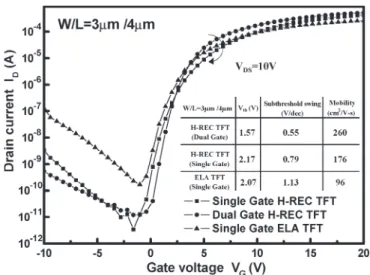
Fig. 3. Transfer characteristics of the single-gate H-REC TFT (square pattern) and the dual-gate H-REC TFT (circle pattern) compared with the single-gate ELA TFT (triangle pattern), operated at saturation region.
obtain a large grain along the lateral growth, it was generally necessary to use laser irradiation shots with higher energy density for continuing the melting duration. This easily leads to the low laser throughput and high cost. In this letter, a 7-µm-length of the Si grain can be laterally grown successfully, just with capping the heat-retaining layer before one shot of laser irradiation. There is only one primary grain boundary located in the active region of poly-Si TFT device, potentially exhibiting high-quality poly-Si grain within the Si island. Furthermore, the poly-Si grains were well-controlled, since the a-Si island was precisely patterned in advance by microlithography and etch processes.
Typical transfer characteristics of the poly-Si TFTs that are crystallized with H-REC and with conventional excimer-laser-annealing (ELA) methods are compared, as shown in Fig. 3. Several important device parameters are also listed in the insert. The field-effect mobility is extracted from the linear region at VDS= 0.1 V. The threshold voltage is defined according
to the criterion ID= (W/L)× 10−8 A at VDS= 0.1 V. The
poly-Si TFT crystallized with H-REC exhibited superior elec-trical characteristic than the conventional ELA poly-Si TFT. As compared with the single-gate poly-Si TFT, the proposed dual-gate H-REC TFT has high field mobility of 260 cm2/V· s
and low subthreshold swing of 0.55 V/dec. It is well known that the characteristics of TFTs are strongly affected by the relationship between the current flow and grain-growth direc-tion (i.e., perpendicular or parallel). The mobility is confined by the grain boundaries in the channel region, because the carrier transportation is obstructed by the boundary potential. The H-REC TFT has superior electrical characteristics due to the single one grain boundary perpendicular to the current path. On the other hand, doping process can reduce the barrier height in the grain boundary effectively, which is according to Seto’s model [12]. Therefore, the dual-gate H-REC TFT, whose single grain boundary within a highly doped region [shown in Fig. 1(d)], can exhibit higher mobility than the single-gate H-REC TFT with a single grain boundary inside the channel [shown in Fig. 1(c)]. The benefit of the dual-gate structure can
724 IEEE ELECTRON DEVICE LETTERS, VOL. 28, NO. 8, AUGUST 2007
Fig. 4. Comparison of mobility degradation for the dual-gate H-REC TFT, the single-gate H-REC TFT, and the single-gate ELA TFT, during the dynamic-stress measurements.
also reduce the lateral electric field at the drain junction and suppress the hot-carrier effect to promote the reliability at the same device dimension [13]–[15].
In order to investigate the electrical stability under the ac operation, TFT devices were subjected to a dynamic stress test for 1000 s. The ac stress pulse applied to the gate electrode and source/drain grounded is also listed in the insert of Fig. 4. Fig. 4 shows the comparison of mobility degradation for three types of poly-Si TFT devices after dynamic stress. It is distinctly observed that both H-REC poly-Si TFTs exhibit extremely low-mobility degradation than the ELA poly-Si TFT. Since defects are frequently present at poly-Si grain boundaries [3], the reduction of the grain boundary in the H-REC poly-Si channel could obtain superior quality of poly-Si film compared to the ELA poly-Si.
IV. CONCLUSION
We have successfully fabricated the high-performance poly-Si TFT with a dual-gate structure by H-REC technology. A 7-µm length of poly-Si grain was laterally grown and precisely controlled by reducing the heat dissipating in the melting silicon islands during the crystallization process. The proposed H-REC TFT exhibits high mobility (∼260 cm2/V· s) and
rather little mobility degradation under ac stress, compared to the conventional ELA TFT. The advantages of the H-REC process are simple laser equipment and controllable grain growth, potentially promising for the active-matrix-display applications.
ACKNOWLEDGMENT
The authors would like to thank Prof. T.-C. Chang, J.-X. Lin, and the research team in ERSO/ITRI for their assistance in the experiments.
REFERENCES
[1] S. D. Brotherton, D. J. McCulloch, J. B. Clegg, and J. P. Gowers, “Excimer-laser-annealed poly-Si thin film transistors,” IEEE Trans.
Elec-tron Devices, vol. 40, no. 2, pp. 407–413, Feb. 1993.
[2] G. K. Giust and T. W. Sigmon, “Self-aligned aluminum top-gate polysili-con thin-film transistors fabricated using laser recrystallization and gas-immersion laser doping,” IEEE Electron Device Lett., vol. 18, no. 8, pp. 394–396, Aug. 1997.
[3] N. H. Nickel, G. B. Anderson, and R. I. Johnson, “Grain-boundary de-fects in laser-crystallized polycrystalline silicon,” Phys. Rev. B, Condens.
Matter, vol. 56, no. 19, pp. 12 065–12 068, Nov. 1997.
[4] R. S. Sposili and J. S. Im, “Sequential lateral solidification of thin sili-con films on SiO2,” Appl. Phys. Lett., vol. 69, no. 19, pp. 2864–2866, Nov. 1996.
[5] C. H. Oh, M. Ozawa, and M. Matsumura, “A novel phase-modulated excimer-laser crystallization method of silicon thin films,” Jpn. J. Appl.
Phys., vol. 37, no. 5A, pp. L492–L495, May 1998.
[6] P. C. van der Wilt, B. D. van Dijk, G. J. Bertens, R. Ishihara, and C. I. M. Beenakker, “Formation of location-controlled crystalline islands using substrate-embedded seeds in excimer-laser crystallization of silicon films,” Appl. Phys. Lett., vol. 79, no. 12, pp. 1819–1921, Sep. 2001. [7] C. H. Kim, I. H. Song, W. J. Nam, and M. K. Han, “A poly-Si TFT
fabricated by excimer laser recrystallization on floating active structure,”
IEEE Electron Device Lett., vol. 23, no. 6, pp. 315–317, Jun. 2002.
[8] Y. Helena, R. Dassow, M. Nerding, K. Mourgues, F. Raoult, J. R. Kohler, T. Mohammed-Brahim, R. Rogel, O. Bonnaud, J. H. Werner, and H. P. Strunk, “High mobility thin film transistors by Nd:YVO4-laser crystal-lization,” Thin Solid Films, vol. 383, no. 1/2, pp. 143–146, Feb. 2001. [9] C. Prat, D. Zahorski, Y. Helenb, T. Mohammed-Brahimb, and
O. Bonnaud, “Excimer laser annealing system for AMLCDs: A long laser pulse for high-performances, uniform and stable TFT,” Proc. SPIE, vol. 4295, pp. 33–37, 2001.
[10] I. H. Song, C. H. Kim, S. H. Kang, and M. K. Han, “A new multi-channel dual-gate poly-Si TFT employing excimer laser annealing recrys-tallization on pre-patterned a-Si thin film,” in IEDM Tech. Dig., 2002, pp. 561–564.
[11] M. Cao, S. Talwar, K. J. Kramer, T. W. Sigmon, and K. C. Saraswat, “A high-performance polysilicon thin-film transistor using XeCl excimer laser crystallization of pre-patterned amorphous Si films,” IEEE Electron
Device Lett., vol. 43, no. 4, pp. 561–567, Apr. 1996.
[12] J. Y. Seto, “The electrical properties of polycrystalline silicon films,”
J. Appl. Phys., vol. 46, no. 12, pp. 5247–5254, Dec. 1975.
[13] J. Y. Park, H. H. Park, K. Y. Lee, H. D. Kim, and H. K. Chung, “Microstructure-controlled SLS poly-Si TFT,” in Proc. Int. Workshop
AMLCD, 2003, pp. 149–152.
[14] Y. Morimoto, Y. Jinno, K. Hirai, H. Ogata, T. Yamada, and K. Yoneda, “Influence of the grain boundaries and intragrain defects on the perfor-mance of poly-Si thin film transistors,” J. Electrochem. Soc., vol. 144, no. 7, pp. 2495–2501, Jul. 1997.
[15] Y. C. Wu, T. C. Chang, P. T. Liu, C. W. Chou, Y. C. Wu, C. H. Tu, and C. Y. Chang, “Reduction of leakage current in metal-induced lateral crystallization polysilicon TFTs with dual-gate and multiple nanowire channels,” IEEE Electron Device Lett., vol. 26, no. 9, pp. 646–648, Sep. 2005.