氮化鎵二維面射型光子晶體分散回饋式雷射之研究
66
0
0
全文
(2) 氮化鎵二維面射型光子晶體分散回饋式雷射之研究 Study of GaN-based Two-Dimensional Surface-Emitting Photonic Crystal Distributed-Feedback Laser. 研 究 生:林立凡. Student:Li-Fan Lin. 指導教授:郭浩中. Advisors:Hao-Chung Kuo. 盧廷昌. Tien-Chang Lu. 國 立 交 通 大 學 光 電 工 程 研 究 所 碩 士 論 文. A Thesis Submitted to Institute of Electro-Optical Engineering College of Electrical Engineering and Computer Science National Chiao Tung University in partial Fulfillment of the Requirements for the Degree of Master in Electro-Optical Engineering June 2007 Hsinchu, Taiwan, Republic of China. 中 華 民 國 九 十 六 年 六 月.
(3) 氮化鎵二維面射型光子晶體分散回饋式雷射之研究. 研究生: 林立凡. 指導教授: 郭浩中 教授. 盧廷昌 教授. 國立交通大學 光電工程研究所. 摘 要 本論文主要是探討氮化鎵二維面射型光子晶體分散回饋式雷射之製做與研究。在模 擬方面,我們是利用平面波展開法來計算元件的光能帶圖。在製作方面,我們利用電子 束微影技術,製作了不同晶格常數的元件(晶格常數從 190 到 300 奈米)。在量測方面, 我們利用光激發系統在室温下進行元件的特性測量,我們觀測到不同的元件(不同的晶 格常數)都會有雷射的發光現象,其臨界激發光能量密度大約為 3.5mJ/cm2 ,雷射波長從 397 至 425 奈米,半高寬約為 1.1Å。除此之外,我們對於其它雷射的特性也做了相關量 測,例如,極化程度(53%)、發散角(<10∘)、雷射發光情形等… 。其中,在光學顯微 鏡的觀測下,我們發現幾乎整個光子晶體的區域都會有雷射發光現象,並且由雷射的發 光頻譜可以得知,此雷射在單一波長下操作。最後,我們也比較了實驗量測及理論模擬 的正規化頻率。由實驗數據可發現其正規化頻率可分為幾個群組,這些群組都可以對應 到相對的理論模擬結果,而這些對應的點則都是位於布里淵區的邊界,這是因為在這些 布里淵區的邊界會滿足布拉格繞射條件。由以上的敘述,說明了我們可以獲得大面積單 模態的氮化鎵藍光面射型雷射。. i.
(4) Study of GaN-based Two-Dimensional Surface-Emitting Photonic Crystal Distributed-Feedback Laser. Student : Li-Fan Lin. Advisor : Dr. H.C. Kuo Dr. T.C. Lu. Institute of electro-optical Engineering National Chiao-Tung University. Abstract In this thesis, we study the fabrication and characteristics of GaN-based two-dimensional surface-emitting photonic crystal distributed-feedback (2D SEPC DFB) laser. We also simulated the band diagram of the PC structure to realize the lasing mechanism by using plane-wave expansion (PWE) method. We fabricated these devices with different lattice constant (from 190nm to 300nm) by using electron-beam lithography (EBL). The laser action of photonic crystal devices was achieved under the optical pumping at room temperature. The clear threshold characteristic was observed at different devices (a=190-300nm). All these devices show a similar threshold pumping energy densities to be about 3.5mJ/cm2. The GaN-based 2D SEPC DFB laser emits violet wavelength (from 397nm to 425nm) with a linewidth of about 1.1Å. In addition, the degree of polarization (53%)、divergence angel (<10 ∘) and emission image of the laser was also measured. In emission image of the laser, we obtain a stimulated emission of GaN-based 2D SEPC DFB laser over a large area. All emission light normal to the sample surface is collected into a spectrometer/CCD, and the lasing spectrum shows just one lasing mode in the whole lasing area. So, it is clear, the single mode GaN-based 2D SEPC DFB laser with large lasing area was demonstrated. Finally, we compare experiment results with simulation results. We are able to classify the normalized frequency into few groups. Different groups of the normalized frequency occur at different points of Brillouin-zone boundary, Γ、M、K points. All points of normalized frequency can exactly correspond to points of Brillouin-zone boundary because the Bragg condition only satisfies at these points.. ii.
(5) 誌謝. 時間飛逝,轉眼間又到了這令人既喜悅又感傷的季節,喜悅的是經過兩年的努力, 終於可以順利畢業,感傷的是要和在一起生活兩年的學長姊、同學以及學弟妹分開,不 過這也是人生中必經的過程。 在這兩年的學習中,學生在專業上及生活上遇到了不少問題,有幸因為老師們、學 長姊、同學及學弟妹熱心的幫忙及協助,使學生得以將問題一一的解決。所以在這裡首 先要感謝王老師的熱心指導,王老師對於實驗上的熱情以及做事謹慎小心的態度,一直 都是學生學習目標。再來要感謝郭老師,記得第一次與郭老師商談選擇實驗室相關的問 題時,郭老師費心回答學生的疑慮以及給了學生許多的建議,也因如此學生才有幸在本 實驗室度過這兩年的研究所生涯。再來也要感謝盧老師對於學生論文上及實驗上的指導 及要求。而在磊晶方面,要感謝黃博、忻宏、明華及俊榮學長的幫忙。在離子佈值方面, 要感謝清大陳建旭學長。 此外,非常感謝我的直屬學長小強及宗鼎,他們不管在實驗或做人處事上,都給了 學生許多的建議,也因為有他們無私的指導,學生才有幸可以學習到許多不同的事物。 當然也要感謝小朱學長,小朱學長對於我的照顧也不在話下。而老余、泓文、佳恩、詒 安、亞銜、厚光、鴻儒、裕鈞及偉倫學長也常常在我有困難時給與協助。學長姐士偉、 清華、小賴、乃方、剛帆、柏傑、志堯、意偵、游敏、文凱及皇伸也給了學生許多的幫 助。另外感謝這兩年來跟我一起努力的好同學孟儒、卓亦、潤琪、家璞、瑞農及碩均, 謝謝你們陪我走過這兩年的歲月,讓我的生活更加多彩多姿,我會記得你們的,記得以 後多聯絡。還有感謝可愛的助理麗君及學弟妹子維、建達、昀恬、怒帆、士嘉、承恩、 柏孝、家銘、伯駿、晁恩及柏源的幫忙,希望以後你們的人生也可以順順利利的。 最後,我要感謝我的家人以及我的女朋友,因為有了你們無怨無悔的支持及鼓勵, 使我在失落時有所慰藉,也使我更加堅強,謝謝你們的付出。. 2007/07. iii. 立凡于.
(6) Contents Abstract (in Chinese)........................................................................................................... i Abstract (in English)............................................................................................................ ii Acknowledgement.................................................................................................................iii Contents................................................................................................................................. iv Table Contents...................................................................................................................... vi Figure Contents.....................................................................................................................vii. Chapter 1. Chapter 2. Overview……………………………………………………………………...1 1.1. Introduction……………………………………………………………. 1. 1.2. Developments of Two-Dimensional Photonic crystal Lasers…………. 2. 1.3. Objective of the Thesis………………………………………………... 4. 1.4. Outline of the Thesis…………………………………………………... 4. Fundamentals of Laser……………………………………………………... 5 2.1. The Theory of DBRs….……………………………………………… 5. 2.2. The Bragg Diffraction In 2D Triangular-Lattice Structure…………... 8. 2.3. Spontaneous and Stimulated Transition………..…………………….. 9. 2.4. Operation Mechanism of Laser………………………..……………... 10. Chapter 3 Fabrication of GaN-based 2D SEPC DFB Laser……..................................14. Chapter 4. 3.1. Electron Beam System……….............................................................. 14. 3.2. Wafer Preparation.................................................................................. 16. 3.3. Process Procedure………………………………………………..…… 16. 3.4. Process Flowchar……………………………………………………... 18. Optical pumping GaN-based 2D SEPC DFB Laser .................................... 20 4.1. Design of GaN-based 2D SEPC DFB Laser….......................................20 4.1.1. Micro-Photoluminescence (μ-PL).............................................. 20. 4.1.2. Calculation of Confinement Factor and Effective Refractive Index ………………………………………………………….. 20 iv.
(7) 4.1.3. Calculation of dielectric constant (εa and εb)………………….. 21. 4.1.4. Simulation of Band Diagram………………………………….. 21. 4.2. Optical Pumping Experiment………………………………................. 22. 4.3. Characteristics of GaN-based 2D SEPC DFB Laser…………….......... 22 4.3.1. Stimulated emission (lasing)....................................................... 22. 4.3.2 Emission images of GaN-based 2D SEPC DFB laser................ 23. 4.4. Chapter 5. 4.3.3. Polarization……………………………………………………. 23. 4.3.4. Divergence Angle………………………………………….….. 23. Comparison between Experiment and Simulation Results…................. 24. Conclusions...................................................................................................... 25. Reference............................................................................................................................... 54. v.
(8) Table Contents Table 3.1 Properties of the electron sources commonly used in electron beam lithography tools…………………………….………………………………………………. 26 Table 3.2 Process flowchart………………………………………………………………. 26. vi.
(9) Figure Contents. Fig. 1.1 Schematic diagram of topical 2D PC cavity........................................................... 27 Fig. 1.2 Spectrum of the laser. The spontaneous emission is shown in the inset................ 27 Fig. 1.3 L-L curve showing the power at the laser wavelength versus the incident pump power…….………………………………………………………………………. 28 Fig. 1.4 Schematic diagram of electrically driven single-cell photonic crystal laser…….. 28 Fig. 1.5 L-I curve of the laser. The lasing spectrum is shown in the inset……………….. 29 Fig. 1.6 Schematic diagram of PC membrane nano-cavity………………………………. 29 Fig. 1.7 Resonance modes of nano-cavities and r /a =0.262±0.004, 0.254±0.004, and 0.246±0.004 from top to bottom……………………...…………………………..30 Fig. 1.8 Schematic structure of the surface-emitting laser with 2D triangular-lattice structure. The inset shows the SEM photograph of the triangular-lattice structure………... 30 Fig. 1.9 L-I characteristic of the 2D PC laser at RT under pulsed condition (repetition period: 1ms, pulse width: 500 ns)………………………………………………………... 31 Fig. 1.10 Lasing spectrum under pulsed condition and the injection current was J=1.56 Jth.31 Fig. 1.11 Schematic diagram of the device structure………………………………………. 32 Fig. 1.12 Lasing spectrum of the device under RT-CW condition………………………… 32 Fig. 1.13 Light output power-current characteristic……………………………………….. 33 Fig. 2.1 Schematic draw of the light reflected from the top and bottom of the thin film.... 33 Fig. 2.2 Schematic diagram of DBR……………………………………………………… 34 Fig. 2.3 Structure of 2D triangular lattice in real space…………………………………... 34 Fig. 2.4 Structure of 2D triangular lattice in reciprocal space……………………………. 35 Fig. 2.5 Triangular reciprocal lattice diagram of in-plane direction at Г point…………... 35 Fig. 2.6 Triangular reciprocal lattice diagram of vertical direction at Г point…………… 36 Fig. 2.7 Triangular reciprocal lattice diagram of in-plane direction at M point………...... 36 vii.
(10) Fig. 2.8 Triangular reciprocal lattice diagram of in-plane direction at K point…………... 37 Fig. 2.9 Electronic transitions between the conduction and valence bands………………. 37 Fig. 2.10 Reservoir with continuous supply and leakage as an analog to a DH active region with current injection for carrier generation and radiative and nonradiative recombination……………………………………………………………………. 38 Fig. 2.11 Illustration of output power versus current for a diode laser……………………..38 Fig. 3.1 Cross-section of a typical electron beam block………………………………….. 39 Fig. 3.2 Schematic diagram of half-structure by MOCVD………………………………..39 Fig. 3.3 Reflectivity spectrum of the half structure with 35 pairs of GaN/AlN DBR structure measured by N&K ultraviolet-visible spectrometer with normal incident at room temperature………………………………………………………………………. 40 Fig. 3.4 CCD image of GaN-based material with SiN film 200nm……………………… 40 Fig. 3.5 SEM image of soft mask pattern............................................................................ 41 Fig. 3.6 SEM image of hard mask pattern........................................................................... 41 Fig. 3.7 Top view SEM image of 2D SE PC DFB laser...................................................... 42 Fig. 3.8 SEM image of Cross-section of 2D SE PC DFB laser........................................... 42 Fig. 3.9 Schematic diagram of nitride structure grown by MOCVD…………………….. 43 Fig. 3.10 1st step of process: deposing SiN film…………………………………………... 43 Fig. 3.11 2nd step of process: soft mask…………………………………………………… 44 Fig. 3.12 3rd step of process: hard mask…………………………………………………... 44 Fig. 3.13 4th step of process: ICP etching…………………………………………………. 45 Fig. 3.14 5th step of process: removing hard mask……………………………………….. 45 Fig. 4.1 Measurement setup of μ-PL system……………………………………………... 46 Fig. 4.2 PL spectrum of as-grown structure………………………………………………. 46 Fig. 4.3 Distribution of electric field in the vertical direction of the device……………... 47 Fig. 4.4 Calculated band diagram of the 2Dtriangular-lattice structure for transverse-electric viii.
(11) (TE) mode……………………………………………………………………….. 47 Fig. 4.5 Measurement setup of optical pumping system…………………………………. 48 Fig. 4.6 Normalized frequency as a function of the lasing wavelength………………… 48 Fig. 4.7 Excitation energy – emission intensity curve (L-I)……………………………… 49 Fig. 4.8 Spectrum of stimulated emission at room temperature………………………….. 49 Fig. 4.9 Excitation energy intensity VS. emission spectrum……………………………... 50 Fig. 4.10 (a) Spontaneous emission image at 0.92Eth , (b) stimulated emission image at 1.47Eth.....................................................................................................................50 Fig. 4.11 Measurement setup for DOP…………………………………………………….. 51 Fig. 4.12 Intensity of laser emission as a function of the angle of the polarizer…………... 51 Fig. 4.13 Measurement setup for divergence angle……………………………………….. 52 Fig. 4.14 Intensity of laser emission as a function of the angle of the fiber position……… 52 Fig. 4.15 Experiment (left) and simulation results (right)…………………………………. 53. ix.
(12) Chapter 1 Overview 1.1 Introduction Nitride-based materials have attracted a great attention in the early 1990s due to the large direct band gap and the promising potential for the optoelectronic devices, such as light emitter diodes (LEDs) and laser diodes (LDs) [1- 7]. In the early 1970s, the crystal growth, basic properties and the fabrication of the prototype of GaN-based light emitting diodes have been studied by Maruska and Tietjen [8], Pankove et al. [9], and Maruska et al. [10]. In 1993 the first prototype high brightness (> 100 rimes greater than previous alternatives, about 1 candela) GaN-based blue LEDs were developed by Nakamura`s group, and then they reported room temperature pulsed [11] and continuous wave (CW) lasing operation [12] of GaN-based blue LD with an emission wavelength of around 400nm in 1996. Recently, Nichia Corporation succeeded in developing high power blue-violet semiconductor laser diodes corresponding to a double-layer disc at more than 10 X record speed/ a quad-layer disc at more than 2 X record speed applied for the next generation DVD recorders and they confirmed that estimated life time exceeded 10,000 hours and stable operation was achieved for 1000 hours with the condition of 320mW pulsed operation at 80°C [13]. Today, blue LEDs are widely used in many applications such as mobile electronics, flat panel displays, Competing storage technologies, automobiles, traffic signals, back light of liquid crystal display, general lighting, large outdoor displays and illumination. The blue LD can serve as the light source of high density data storage in high definition digital versatile disk (HD-DVD). The big market of HD-DVD has shown up the importance of blue LDs. Besides, the blue and violet LDs 1.
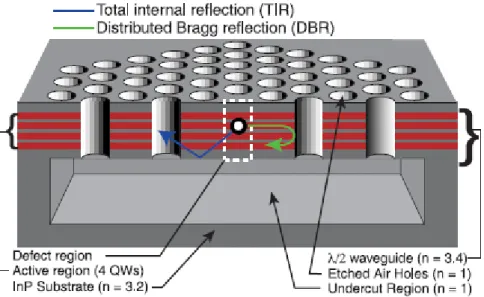
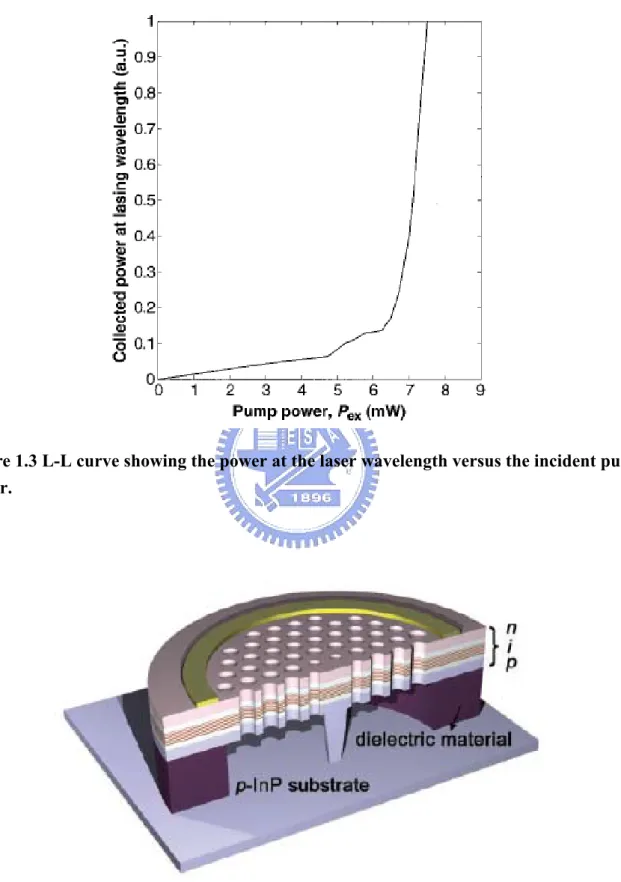
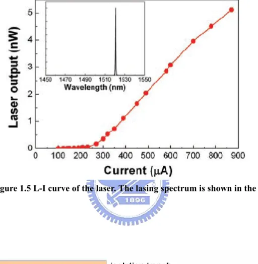
(13) may have many other possible markets, such as high brightness projector, high speed printer, medical field and others.. 1.2 Developments of Two-Dimensional Photonic crystal Lasers Semiconductor 2D PC laser provide mode confinement at a characteristic length comparable to an optical wavelength and have emerged as a versatile building block to construct photonic circuitry. Such structures can act not only as a passive waveguide or resonator to direct the wave propagation but also as an active medium to control light emission [14]. They are some structures to forming the 2D PC laser such as (i) 2D PC nano-cavity laser, (ii) 2D PC band edge laser.. 2D PC Nano-Cavity Lasers In 1994, P. R. Berman et al. first presented that photonic crystal (PC) can be a reflected mirror around the cavity of laser [15]. In 1999, 2D optically pumped PC cavity laser was demonstrated by O. Painter [16]. The optical cavity consists of a half-wavelength thick waveguide for vertical confinement and a 2D PC mirror for lateral localization. A defect in the 2D PC is introduced to trap photons inside a volume of 2.5 cubic half-wavelength, approximately 0.03 cubic micrometers. The laser is fabricated in the InGaAs material system, and the peak emission wavelength is 1.55 micrometers. The figure 1.1 is the structure of PC laser. The spectrum of the laser with linewidth about 0.2nm is shown in Fig. 1.2 and the light-output and light-in power (L-L) curve is shown in Fig. 1.3. In 2004, electrically driven single-cell 2D PC laser (λ=1519.7nm) was demonstrated by Hong-Gyu Park et al. [17]. A sub-micrometer-sized semiconductor post is placed at the center of the single-cell photonic crystal resonator and the thickness of the semiconductor slab is 282.5 nm as shown in Fig. 1.4. Electrons are 2.
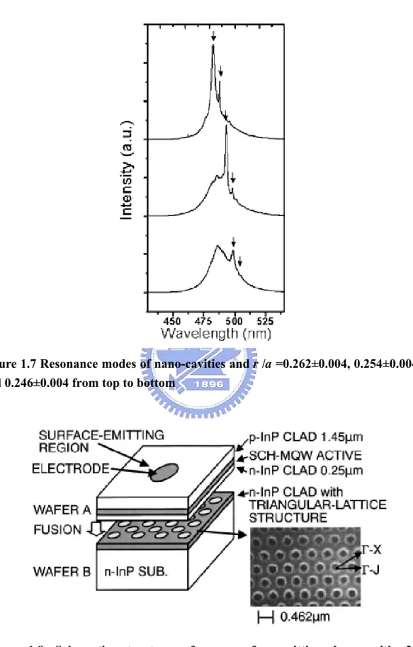
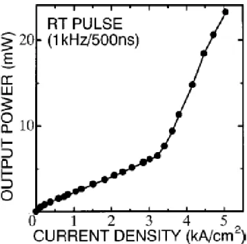
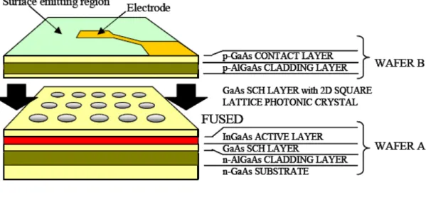
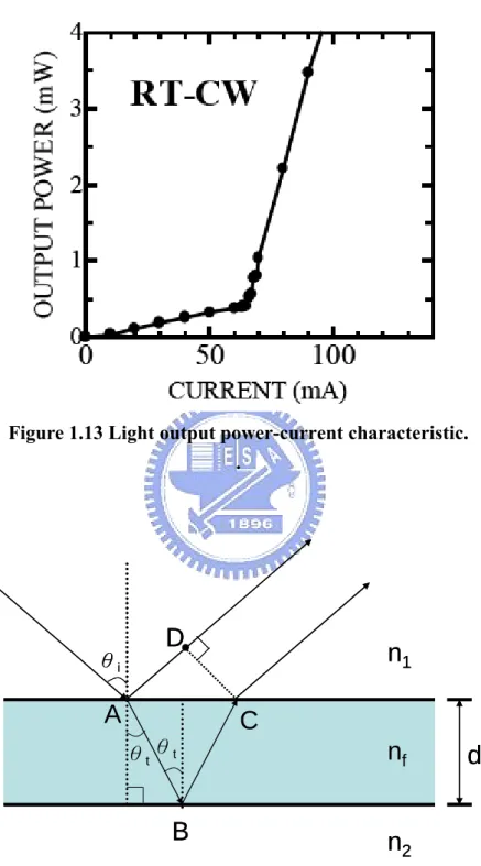
(14) supplied laterally from the top electrode, whereas holes are injected directly through the bottom post. The light-current (L-I) curve of the laser is shown in Fig. 1.5. In 2005, GaN-based blue (about 488nm) photonic crystal membrane nano-cavity with Q factor about 800 was reported by Y. S. Choi et al. [18].The membrane layer consists of a 44 nm unintentionally (uid) doped GaN top cladding, five InGaN quantum wells (QWs), a 14 nm uid GaN bottom cladding, and a 30 nm Al0.15Ga0.85N insulating layer. The total membrane thickness was designed to be 140 nm as shown in Fig. 1.6. Some resonance modes from the nano-cavities with lattice constant 180nm are shown in Fig. 1.7.. 2D PC Band Edge Lasers In 1999, the 2D PC band edge laser with semiconductor QW under pulsed condition was reported by Noda et al. [19]. The PC has a triangular-lattice structure composed of InP and air holes, which is integrated with an InGaAsP/InP multiple-quantum-well active layer by a wafer fusion technique. The sample structure and SEM image of triangular lattice PC structure is shown in Fig. 1.8. The L-I curve and lasing spectrum are shown in Figs. 1.9 and 1.10, respectively. In 2004, they successfully reported the 2D PC band edge laser under room temperature continuous wave (RT-CW) operation [20]. The device structure, lasing spectrum and light output power-current characteristic are shown in Figs. 1.11, 1.12 and 1.13, respectively. However, the GaN-based 2D PC laser on both structures has not been demonstrated; and the 2D PC band edge laser has been repeatedly considered as potential candidates for perfect single-mode emission over a large area, high output power, and surface emission with a very narrow divergence angle. Therefore, my group makes effort on GaN-based 2D PC laser and makes it.. 3.
(15) 1.3 Objective of the Thesis In this thesis, we report the fabrication of GaN-based two-dimensional (2D) photonic crystal (PC) distributed-feedback surface-emitting (DFBSE) laser using the AlN/GaN DBRs as the bottom mirror and periodical nano-holes which to form a PC, and demonstration of the laser operation under optical pumping at room temperature. We also present the characteristics of optical pumping GaN-based 2D PC DFBSE laser such as excitation energy – emission intensity characteristic (L-I), emission image of laser, polarization, divergence angle. In addition, the simulation of band diagram of triangular lattice PC was calculated by R-Soft. Finally, we discuss the experiment results and compare them with the simulated band diagram.. 1.4 Outline of the Thesis This thesis is organized in the following manner. In chapter 2, the formation, operation mechanism and applications of 2D PC DFB SE laser and simulation method are briefly introduced. In chapter 3, the fabrication of GaN-based 2D PC DFB SE with (EBL) is presented. In chapter 4, we discuss the characteristics of GaN-based 2D PC DFB SE laser. Finally, chapter 5 is the conclusion and future work.. 4.
(16) Chapter 2 Fundamentals of Laser 2.1 The Theory of DBRs The DBRs are a simplest kind of periodic structure, which is made up of a number of quarter-wave layers with alternately high- and low- index materials. Therefore, it’s necessary to know the theory of quarter-wave layer before discussing the DBRs. Quarter-wave layer [21-22] Consider the simple case of a transparent plate of dielectric material having a thickness d and refractive index nf, as shown in Fig 2.1. Suppose that the film is nonabsorbing and that the amplitude-reflection coefficients at the interfaces are so low that only the first two reflected beams (both having undergone only one reflection) need be considered. The reflected rays are parallel on leaving the film and will interference at image plane. The optical path difference (P) for the first two reflected beam is given by. and since. P = nf [( AB ) + ( BC )] − n1( AD ). (2.1). ( AB ) = ( BC ) = d cos θt. (2.2). 2 n fd − n1( AD ) cos θt. (2.3). ( AD ) = ( AC ) sin θi. (2.4). P=. also Using Snell’s Law. ( AD ) = ( AC ). nf sin θt ni. ( AC ) = 2d tan θt. The expression for P now becomes or finally. P=. 2 nfd (1 − sin 2 θt ) cos θt. P = 2nfd cos θ. 5. (2.5) (2.6). (2.7) (2.8).
(17) The corresponding phase difference (δ) associated with the optical path length difference is then just the product of the free-space propagation number and P, that is, KoP. If the film is immersed in a single medium, the index of refraction can simply be written as n1=n2=n. It is noted that no matter nf is greater or smaller than n, there will be a relative phase shift π radians. Therefore,. d cos θt = (2m + 1). δ=. or. 4πnf. λ0. λf. (2.9). 4. ( nf 2 − n 2 sin 2 θi ) 2 ± π. (2.10). The interference maximum of reflected light is established when δ=2mπ, in other words, an even multiple of π. In that case Eq. (2.9) can be rearranged to yield. [maxima]. d cos θt = (2m + 1). λ0 4nf. (m = 0, 1, 2,…). (2.11). The interference maximum of reflected light is established when δ=(2m±1)π, in other words, an odd multiple of π. In that case Eq. (2.9) can be rearranged to yield. [minima]. d cos θt = 2m. λ0 4nf. (m = 0, 1, 2,…). Therefore, for an normal incident light into thin film, the interference maximum of reflected light is established when d = λ0/4nf (at m=0). Based on the theory, a periodic structure of alternately high- and low- index quarter-wave layer is useful to be a good reflecting mirror. This periodic structure is also called Distributed Bragg Reflectors (DBRs). Distributed Bragg Reflectors (DBRs) [23- 28] DBRs serve as high reflecting mirror in numerous optoelectronic and photonic devices such as VCSEL. There are many methods to analyze and design DBRs, and the matrix method is one of the popular one. The calculations of DBRs are entirely described in many optics books, and the derivation is a little too long to write in this thesis. Hence, we put it in simple to understand DBRs. Consider a distributed Bragg 6. (2.12).
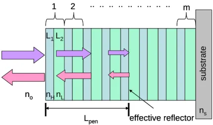
(18) reflector consisting of m pairs of two dielectric, lossless materials with high- and lowrefractive index nH and nL, as shown in Fig 2.2. The thickness of the two layers is assumed to be a quarter wave, that is, L1 =λB/4nH and L2 =λB/4nL, where theλB is the Bragg wavelength. Multiple reflections at the interface of the DBR and constructive interference of the multiple reflected waves increase the reflectivity with increasing number of pairs. The reflectivity has a maximum at the Bragg wavelength λB. The reflectivity of a DBR with m quarter wave pairs at the Bragg wavelength is given by ns nL 2 p ⎞ ⎛ ⎜1− ( ) ⎟ ⎟ R = ⎜ no nH ⎜ 1 + ns ( nL ) 2 p ⎟ ⎜ ⎟ ⎝ no nH ⎠. (2.13). where the no and ns are the refractive index of incident medium and substrate.The high-reflectivity or stop band of a DBR depends on the difference in refractive index of the two constituent materials, △n (nH-nL). The spectral width of the stop band is given by. Δλstopband =. 2λBΔn πneff. (2.14). where neff is the effective refractive index of the mirror. It can be calculated by requiring the same optical path length normal to the layers for the DBR and the effective medium. The effective refractive index is then given by neff = 2(. 1 1 −1 + ) nH nL. (2.15). The length of a cavity consisting of two metal mirrors is the physical distance between the two mirrors. For DBRs, the optical wave penetrates into the reflector by one or several quarter-wave pairs. Only a finite number out of the total number of quarter-wave pairs are effective in reflecting the optical wave. The effective number of pairs seen by the wave electric field is given by meff ≈. 1 nH + nL nH − nL tanh( 2m ) 2 nH − n L n H + nL 7. (2.16).
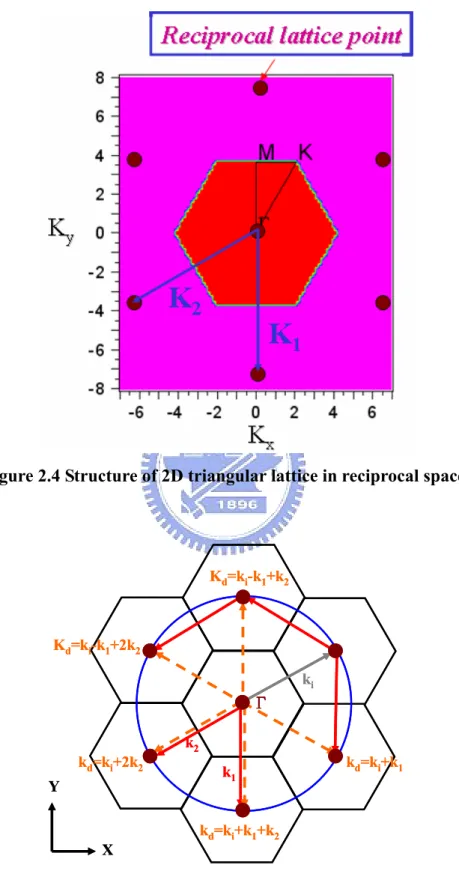
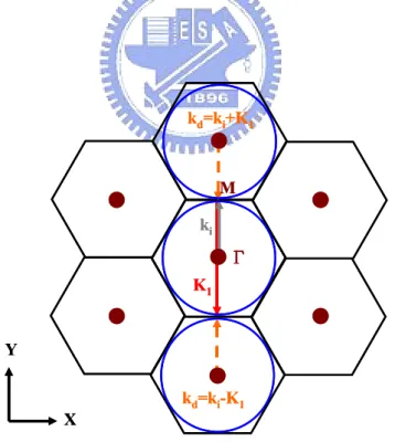
(19) For very thick DBRs (m→∞) the tanh function approaches unity and one obtains meff ≈. 1 nH + nL 2 nH − nL. (2.17). Also, the penetration depth is given by Lpen =. L1 + L 2 tanh( 2mr ) 4r. (2.18). where r = (n1-n2)/ (n1+n2) is the amplitude reflection coefficient. For a large number of pairs (m→∞), the penetration depth is given by Lpen ≈. L1 + L 2 L1 + L 2 nH + nL = 4r 4 nH − nL. (2.19). Comparison of Eqs. (2.17) and (2.19) yields that Lpen =. 1 meff ( L1 + L 2) 2. (2.20). The factor of (1/2) in Eq. (2.20) is due to the fact that meff applies to effective number of periods seen by the electric field whereas Lpen applies to the optical power. The optical power is equal to the square of the electric field and hence it penetrates half as far into the mirror. The effective length of a cavity consisting of two DBRs is thus given by the sum of the thickness of the center region plus the two penetration depths into the DBRs.. 2.2 Bragg Diffraction In 2D Triangular-Lattice Structure[29][ 30 ] In there, we consider the sample structure has three layers. The 2D triangular-lattice structure is in the middle layer. The real lattice and reciprocal lattice of 2D triangular-lattice structure is shown in Fig. 2.3 and 2.4, respectively. K1 and K2 are the Bragg vectors with magnitude |K|=2π/a, where a is lattice constant. We consider the TE mode in the 2D PC structure. The incident lightwave and diffracted lightwave must be satisfied the relationship, kd=ki+q1K1+q2K2,. q1,2=0, ±1, ±2, …. ω d = ωi 8. (2.21) (2.22).
(20) where kd is xy-component wave vector of diffracted lightwave, ki is xy-component wave vector of incident lightwave, q12 is order of coupling. In Eq. (2.22), ωd is the frequency of diffracted lightwave and ωi is the frequency of incident lightwave. The Eq.. (2.21). and. Eq.. (2.22). represent. the. phase-matching. condition. and. constant-freqency condition. First, we consider the lattice point Γ in first Brillouin zones of the structure as shown in Fig. 2.5. Figure 2.5 shows that lightwaves are diffracted in five different Γ-Γ directions such as kd=ki+K1, kd=ki+K1+K2, kd=ki+2K2, kd=ki-K1+2K2, kd=ki-K1+K2, in addition, kd = ki+K1 also satisfy the Bragg condition as shown in Fig. 2.6. So, in this case, the incident lightwave can couple with lightwave of the five different directions in in-plane which like a cavity and the coupling light also can emit normal to the sample surface due to the first Bragg diffraction. Second, we consider the M point in first Brillouin zones of the structure as shown in Fig. 2.7. The diffraction condition is expressed as kd=ki+K1 and kd=ki-K1. Here, the kd, ki+K1 and kd=ki-K1 must be parallel to the Γ-M direction to satisfy the diffraction condition. In this case, the incident lightwave only coupled two waves that propagate in the forward and backward directions and the cavity can exist in each of the three different directions. This is similar to the 1D DFB laser. Third, the K point in first Brillouin zones of the structure must be considered as shown in Fig. 2.8. In this case, the diffraction condition is expressed as, kd=ki+K1, kd=ki+K2, and the diffraction waves are not parallel to the Γ-K direction. It is different from the others. There are six directions in Γ-K direction and we can know that two different cavities exist simultaneously in the different Γ-K direction from Fig. 2.8. The lasing mode is not clear due to the couple waves are emitted in the three different directions. Finally, the lattice points of higher Brillouin zones of the structure are not described in here because those are similar to the lattice points of first Brillouin zones of the structure.. 2.3 Spontaneous and Stimulated Transition [31] 9.
(21) In here, we can consider only a single level in both the conduction and valence bands in semiconductor. In Fig. 2.9, there are four basic mechanism of electron generation/recombination must be considered: (i) spontaneous emission, (ii) stimulated absorption, (iii) stimulated emission, (iv) nonradiative recombination. The solid circles represent electrons and the open circles represent holes. The first case (Rsp) represents the electron in conduction band recombining with a hole in valence band spontaneously to generate a photon. If a lager number of photon is generated, the emission time and direction would be random, and the emission is not coherent radiation light. This is the primary mechanism of LED, in which photon feedback is not provided. The second case (R12) represents the electron in valence band absorbs the energy of pumping source to generate the electron in conduction band while leaving a hole in the valence band. The third case (R21) is the same as the second, only the sign of the interaction is reversed. An incident photon gets into the system, stimulate the electron and hole to recombine, and generate a new photon. This is an important mechanism because it is necessary for lasers. The fourth case represents several nonradiative ways, a conduction band electron can recombine with a valence band hold without generating any photons such as nonradiative recombination centers and Auger recombination.. 2.4 Operation Mechanism of Laser[29-30][31- 35] The operation of a semiconductor lasers, can be understood by observing the flow of carriers into its active region, the generation of photons due to the recombination of some of these carriers, and the transmission of some of these photons out of the optical cavity. These dynamics can be described by a set of rate equations, one for the carriers and one for the photons in each of the optical modes.. Carrier density rate equation. The carrier density in the active region is governed by a dynamic process. In fact, we can compare the process of establishing a certain steady-state carrier density in the active region to that of establishing a certain water level in a reservoir which is being simultaneously filled and drained. This is shown schematically in Fig. 2.10. As we 10.
(22) proceed, the various filling (generation) and drain (recombination) terms illustrated will be defined. The current leakage illustrated in Fig. 2.8 contributes to reducing ηi and is created by possible shunt paths around the active region. The carrier leakage, Rl, is due to carriers “splashing” out of the active region (by thermionic emission or lateral diffusion if no lateral confinement exists) before recombining. Thus, this leakage contributes to a loss of carriers in the active region that could otherwise be used to generate light. For the DH active region, the injected current provides a generation term, and various radiative and nonradiative recombination process as well as carrier leakage provide recombination terms. Thus, we can write the carrier density rate equation, dN = G gen − Rrec dt. (2.23). where N is the carrier density (electron density), Ggen is the rate of injected electrons and Rrec is the ratio of recombining electrons per init volume in the active region. Since there areηi I/q electrons per second being injected into the active region, G gen =. ηi I qV. , where V is the volume of the active region. The recombination process is. complicated and several mechanisms must be considered. Such as, spontaneous recombination rate, Rsp ~ BN2, nonradiative recombination rate, Rnr, carrier leakage rate, Rl, (Rnr + Rl = AN+CN3), and stimulated recombination rate, Rst. Thus we can write Rrec = Rsp + Rnr + Rl +Rst. Besides, N/τ ≡ Rsp + Rnr + Rl, where τ is the carrier lifetime. Therefore, the carrier density rate equation could be expressed as carrier density rate equation. dN η i I N = − − Rst dt qV τ. Photon density rate equation. Now, we describe a rate equation for the photon density, Np, which includes the photon generation and loss terms. The photon generation process includes spontaneous recombination (Rsp) and stimulated recombination (Rst), and the main photon generation term of laser above threshold is Rst. Every time an electron-hole pairs is stimulated to recombine, another photon is generated. Since, the cavity volume occupied by photons, Vp, is usually larger than the active region volume 11. (2.24).
(23) occupied by electrons, V, the photon density generation rate will be [V/Vp]Rst not just Rst. This electron-photon overlap factor, V/Vp, is generally referred to as the confinement factor, Γ. Sometimes it is convenient to introduce an effective thickness (deff), width (weff), and length (Leff) that contains the photons. That is, Vp=deffweffLeff. Then, if the active region has dimensions, d, w, and La, the confinement factor can be expressed as, Γ=ΓxΓyΓz, whereΓx = d/deff, Γy = w/weff, Γz = La/Leff. Photon loss occurs within the cavity due to optical absorption and scatting out of the mode, and it also occurs at the output coupling mirror where a portion of the resonant mode is usually couple to some output medium. These net losses can be characterized by a photon (or cavity) lifetime, τp. Hence, the photon density rate equation takes the form dN p. photon density rate equation. dt. = Γ Rst + Γ β sp Rsp −. Np. (2.25). τp. where βsp is the spontaneous emission factor. As to Rst, it represents the photon-stimulated net electron-hole recombination which generates more photons. This is a gain process for photons. It is given by ⎛ dN p ⎜⎜ ⎝ dt. ΔN p ⎞ ⎟⎟ = R st = = v g gN p Δt ⎠ gen. (2.26). where vg is the group velocity and g is the gain per unit length. Now, we rewrite the carrier and photon density rate equations. dN η i I N = − − v g gN p dt qV τ. carrier density rate equation. photon density rate equation. dN p dt. = Γ v g g N p + Γ β sp R sp −. (2.27). Np. τp. Output power versus driving current. The characteristic of output power versus driving current (L-I characteristic) in a laser diode can be realized by using the rate equation Eq. (2.29) and (2.30). Consider the below threshold (almost threshold) steady-state (dN/dt = 0) carrier rate equation, the Eq. (2.29) is given by. η i I th qV. = (Rsp + Rnr + Rl )th =. 12. N th. τ. . While the driving current. (2.28).
(24) is above the threshold (I>Ith), the carrier rate equation will be. above threshold carrier density rate equation. ( I − I th ) dN = ηi − v g gN p dt qV. (2.29). From Eq. (2.31), the steady-state photon density above threshold where g = gth can be calculated as steady state photon density. Np =. η i ( I − I th ). (2.30). qv g gthV. The optical energy stored in the cavity, Eos, is constructed by multiplying the photon density, Np, by the energy per photon, hν, and the cavity volume, Vp. That is Eos = NphνVp. Then, we multiple this by the energy loss rate through the mirrors, vgαm = 1/τm, to get the optical power output from the mirrors, P0 = vgαmNphνVp. By using Eq. (2.30) and (2.32), and Γ=V/Vp, we can write the output power as the following equation output power. ⎛ αm PO = η i ⎜⎜ ⎝αi + αm. ⎞ hν ⎟⎟ ( I − I th ) ⎠ q. η iα m , the Eq. (2.33) can be simplified as α iα m hν Thus, the ηd can be expressed as PO = η d ( I − I th ). (2.31). Now, by defining η d =. q. differential quantum efficiency. ⎡ q ⎤ dP. ηd = ⎢ ⎥ O ⎣ hν ⎦ dI. (I > Ith). (2.32). (I > Ith). (2.33). In fact, ηd is the differential quantum efficiency, defined as number of photons out per electron. Besides, dPo/dI is defined as the slope efficiency, Sd, equal to the ratio of output power and injection current. Figure 2.11 shows the illustration of output power vs. current for a diode laser. Below threshold only spontaneous emission is important; above threshold the stimulated emission power increase linearly with the injection current, while the spontaneous emission is clamped at its threshold value.. 13.
(25) Chapter 3 Fabrication of GaN-based 2D SEPC DFB Laser 3.1 Electron-Beam System [36][37] The technique of EBL is using electron beam to generate patterns on a surface and the De broglie relationship (λ < 0.1nm for 10-50keV electrons) to avoid the diffraction limit. So the primary advantage of this technique is that it can beat the diffraction limit of light and create a pattern which only has few nanometers line-width without any mask. The first EBL machines, based on the scanning electron microscope (SEM), were developed in the 1960s. The EBL system usually consists of electron gun, beam blanker for controlling the state of beam, electron lenses for focus the electrons beam, stage and computer control system as shown in Fig. 3.1. Electron Sources Electrons can be emitted from a conductor either by heating the conductor with a sharp point where the electrons obtain sufficient energy from the thermal source to overcome the work function of the conductor (thermal emission sources) or by applying a strong electric field where the electrons can tunnel through the work function (field emission sources). There are three key parameters of the electrons source such as virtual source size, brightness, and the energy spread of the emitted electrons.. The virtual source size determines the number of the lenses in order to form a small spot size at the target. Brightness is similar to the intensity of light optical, so the brighter the electron source has a higher current in the electron beam. The electrons beam with the wide energy spread is similar to white light which has one more wavelength while a beam with a narrow energy spread can be comparable to monochromatic light. Table 3.1 shows the properties of common electrons sources. For many years the normal thermal emission source for lithography optics was formed by using loop of tungsten wire heated white hot by passing a current. Tungsten was chosen for it did not melt or evaporate at high temperature. Unfortunately, this source had a large energy spread caused by the very high operating temperature (2700K) and it was not very bright. Recently, lanthanum hexaboride has become the cathode because it has a very low work function and a high brightness. The electrons beam current for thermal emission source is dependent on operating temperature. Higher temperature can deliver greater electrons beam current (high bright) but the tradeoff is an 14.
(26) exponentially decreasing lifetime due to thermal evaporation of the cathode material. Field emission source usually consist of a tungsten needle with a sharper point and the radius less than 1μm. This tip has sufficient electric field to pull electrons out of the metal. Although cold field emission source has been widely used in electron microscopes but it has some problem for EBL due to their instability with regard to short term noise as well as long term drift. Although the field emission sources have some disadvantages for EBL, but now a technology is available to EBL is the thermal field emission source. It combines a field emission source with sharp tungsten and the heating of the thermal source. Because the tip operates at 1800K, it is less sensitive to gases in the environment and can achieve stable operation for months at a time. Electron Lenses The electrostatic forces or magnetic forces can focus the electrons beam. Although the electron lenses is similar to optical lenses in principle but there are some differences. Besides in some special cases, electron lenses just can be made to converge, not diverge. In addition, the quality of electron lenses in term of aberrations is poor compares with optical lenses. The field size and convergence angle that can be used is limited by the poor quality of electron lenses. The two types of aberrations critical to EBL are spherical aberrations and chromatic aberrations. The spherical aberrations mean the out zones of the lens focus more strongly than the inner zones. The chromatic aberrations means electrons of slightly different energies get focused at different image planes. Both types of aberrations can be limited by reducing the convergence angle of the system, so the electron beam is confined to the center of the lenses. Beam Blanker The beam blanker can bank or turn the beam on or off. It usually consists of a pair of plates set up as a simple electrostatic deflector. One or both plates are linked to a blanking amplifier with a fast response time. A voltage is applied across the plates to turn the beam off. This is necessary when the electrons beam must move from one part of the sample to another. Stage & Computer Control System The stage can control the sample smoothly motion at high magnifications. It is important for EBL because the sample must move from one location to another seamlessly. The computer control system can control the stage moving to the position which is you want and can control the beam blanker to turn on or off. Also, the 15.
(27) compute control system can design any pattern by using GDS software.. 3.2 Wafer Preparation MOCVD grown structure and its reflectivity spectrum. The nitride heterostructure of GaN-based MCLED was grown by metal-organic chemical vapor deposition (MOCVD) system (EMCORE D-75) on the polished optical-grade c-face (0001) 2’’ diameter sapphire substrate, as shown in Fig. 3.2. Trimethylindium (TMIn), Trimethylgallium (TMGa), Trimethylaluminum (TMAl), and ammonia (NH3) were used as the In, Ga, Al, and N sources, respectively. Initially, a thermal cleaning process was carried out at 1080°C for 10 minutes in a stream of hydrogen ambient before the growth of epitaxial layers. The 30nm thick GaN nucleation layer was first grown on the sapphire substrate at 530oC, then 2µm thick undoped GaN buffer layer was grown on it at 1040oC. After that, a 35 pairs of quarter-wave GaN/AlN structure was grown at 1040oC under the fixed chamber pressure of 100Torr and used as the high reflectivity bottom DBR. Finally, the 5λ active pn-junction region was grown atop the GaN/AlN DBR, composed typically of ten In0.2Ga0.8N quantum wells (LW=2.5 nm) with GaN barriers (LB=7.5 nm), and surrounded by 560nm thick Si-doped n-type GaN and 200nm thick Mg-doped p-type GaN layers. The reflectivity spectrum of the half structure with 35 pairs of GaN/AlN DBR structure was measured by the n&k ultraviolet-visible spectrometer with normal incident at room temperature, as shown in Fig. 3.3. The reflectivity spectrum centered at 430nm and stopband width of about 28nm.. 3.3 Process Procedure Initial clean (I.C.). During process of GaN-based nano-cavity laser, four basic skills will be frequently used. First is the initial clean (I.C.), second is plasma enhanced chemical vapour deposition (PECVD) technique, third is EBL technique and fourth is inductively coupled plasma - reactive ion etching (ICP-RIE) technique. The purpose of the I.C. is to remove the small particle, and organism on the sample surface. The steps of I.C. are described as below. 1. Degreasing by ultrasonic baths in acetone (ACE) 5min. 16.
(28) 2. Dipping by ultrasonic baths in isopropyl alcohol (IPA) 5min for organism removed. 3. Rising in de-ionized water (D.I. water) 5min for surface clean. 4. Blowing with N2 gas for surface drying. 5. Baking by hot plate 120oC, 5min, for wafer drying. PECVD (SAMCO PD220). The purpose of PECVD technique is to form a SiN film for hard mask as shown in Fig. 3.4. The details of PECVD technique are described as below. 1. Initial clean 2. SiN film deposition : SiHl4/Ar : 20sccm NH3 : 10sccm N2 : 490sccm Temperate : 300℃ RF power : 35W Pressure :100Pa Time : 20min for depositing SiN 200nm EBL. The purpose of the EBL is to define the pattern on the photoresist (PMMA) (soft mask) is shown in Fig. 3.5. In the process of EBL, a special positive photoresist PMMA (A3) was used. These EBL techniques are described as below. 1. Spin coating by photoresist : PMMA (A3). a. first step : 1000 rpm for 10sec. b. second step : 5000 rpm for 90sec. 2. Hard bake : hot plate 120oC, 1hr. 3. Exposure : Beam voltage : 10KeV Writefield size : 50μm Dot dose : 0.08pAs 4. Development : dipping in IPA : MIBK(3 : 1) 50sec. 5. Fixing : rising in IPA 30sec.. 17.
(29) 6. Blowing with N2 gas for drying. 7. Hard bake : hot plate 120oC, 4min. ICP-RIE (Oxford Plasmalab system 100). The soft mask was transfered to SiN film to form the hard mask by using ICP-RIE as shown in Fig. 3.6. These ICP-RIE techniques are described as below. 1. SiN film etching: Ar/O2: 5sccm CHF3: 50sccm Forward power: 150W Pressure: 7.5*10-9Torr Temperature: 20℃ Time: 100 second for etching SiN film 200nm 2. Initial clean for remove soft mask ICP-RIE (SAMCO RIE-101PH). The purpse of the ICP-RIE techique is to form the PC layer on GaN. The hard mask was transferred to GaN by using ICP-RIE techique. Figure 3.7 are shown the SEM image of top view of 2D SE PC DFB laser, respectively. These ICP-RIE techniques are described as below. 1. P-GaN etching: Ar : 30sccm Cl2 : 45sccm ICP power : 400W Bias power : 40W Pressure : 0.66Pa Time:120sec. for etching P-GaN 400nm 2. Dipping BOE 40sec. for remove hard mask 3. Polishing sapphire for optical pumping. 3.4 Process flowchart Figure 3.8 show the schematic diagram of nitride structure grown by MOCVD. The nano-cavity laser was fabricated by few process steps. In the beginning, the hard mask SiN 200nm was deposited by PECVD as shown in Fig. 3.9. Then PMMA layer 18.
(30) (150nm) was spun by spinner and exposed using E-beam writer to form soft mask as shown in Fig. 3.10. The pattern on soft mask was transferred to SiN film to form the hard mask by using ICP-RIE (Oxford Plasmalab system 100), and then the PMMA layer was removed by dipping ACE as shown in Fig. 3.11. The pattern on hard mask was transferred to GaN by using ICP-RIE (SAMCO RIE-101PH) to form the PC layer as shown in Fig. 3.12. Finally, the sample dips in BOE to remove the hard mask as shown in Fig. 3.13. To completed describe the process flowchart, each process condition is entirely list in the table 3.2.. 19.
(31) Chapter 4 Optical pumping GaN-based 2D SEPC DFB Laser 4.1 Design of GaN-based 2D SEPC DFB Laser In this section, we introduce the method to design the GaN-based 2D SEPC DFB laser. For PC laser, the band diagram of PC is important because the normalized frequency, which is determined by the lasing wavelength and the lattice constant of PC, could be obtained from the band diagram. Therefore, we can obtain the lattice constant if the lasing wavelength is determined and this lasing wavelength must correspond to emission wavelength of the active layer. In additional, the Bragg condition is satisfied at Brillouin-zone boundary, Γ, K and M point. At these points, light waves can have opportunity to diffract normally to the surface which was described in section 2.2. Therefore, we can design a GaN-based 2D SEPC DFB laser operating at the designate lasing wavelength with the optimized lattice constant at Brillouin-zone boundary, Γ、K and M point, which can be defined in the photonic band diagram. In this research, we choose the lasing wavelength from micro-photoluminescence emission peak (~425nm) first. Here, we fix the r/a=0.28 for the calculation of the band diagram and the band diagram of PC obtained by using plan-wave expansion (PWE). In order to cover the most points satisfying Bragg condition, the optimized normalized frequency range was chosen from 0.45 to 0.7 which corresponds to the lattice constant range is from 190nm to 300nm for this lasing wavelength. The detail of calculation will be described below. 4.1.1 Micro-Photoluminescence (μ-PL) The μ-PL emission of the as-grown structure must be measured because the lasing wavelength must correspond to emission wavelength of the active layer.. The μ-PL emission is excited by a 325nm He-Cd laser with a spot size of about 3μm diameter. This measurement setup is similar to optical pumping system expects excitation (laser) source as shown in Fig. 4.1. By using the microscopy system, the emission light can be collected into a spectrometer/CCD with a spectral resolution of about 0.1nm for spectral output measurement. The Fig. 4.2 shows the μ-PL emission of the as-grown structure. The μ-PL emission range is from 395nm to 440nm and the peak wavelength is 425nm. 4.1.2 Calculation of Confinement Factor and Effective Refractive Index We calculate the band diagram of the lasing modes by using the method of the 2D 20.
(32) plan-wave expansion (PWE). But the 2D PWE assumes an infinite length in the 3D structure. In fact, our device is 3D structure, and the depths of nano-holds are not infinite. This means we should do some modification to parameters describing our structure and then bring them into the method of 2D PWE to match real condition. Therefore, we further consider some parameters such as confinement factor (Γg) and effective refractive index (neff). We can use the Γg and neff to calculate the dielectric constant for nano-hole (εa) and the background (εb) for 2D PWE calculation [29] The Γg means the ratio of light confined within the 2D PC structure to light confined within the entire device. The neff means the refractive index of the entire device which concludes PC. These two parameters can be obtained by solving the distribution of the electric field in the direction normal to the device surface using the software of Lastip. The result is shown in Fig. 4.3. From the result, we can estimate the Γg and neff values that are 0.613 and 2.2, respectively. 4.1.3 Calculation of dielectric constant (εa and εb) We obtain the parameter Γg and neff in section 4.1.2. Then, we determine εa and εb using two conditions: [29] n eff = fε a + (1 − f )ε b. (4.1). Δε = ε b − ε a = Γg (ε mat − ε air ). (4.2). 2. Where, the f is a filling factor. In our device, the f is equal to f =. 2πr 2. 3a 2 The εmat and εair are dielectric constant of GaN (=2.52) and air (=12), respectively.. Then, the value of εa (2.408) and εb (5.63) is obtained. 4.1.4 Simulation of Band Diagram In section 4.1.2-3, we have obtained the εa and εb. Then, we use the result to calculate the band diagram of the 2D triangular-lattice structure with r/a=0.28 using RSoft. Figure 4.4 shows the calculated band diagram of the 2D triangular-lattice structure for transverse-electric (TE) mode. It can be expected that the lasing occurs at special points such as Brillouin-zone boundary because the Bragg condition is satisfied and the mode density is high at these points. At these lasing points, wave can propagate in different directions and couple each other. For example, at Γ1 point, the. wave can propagate in six different directions and couple in all six different directions to form a cavity. Then the light will emit in the direction perpendicular to the PC surface (down and up) because the Bragg condition is also satisfied in these 21. (4.3).
(33) directions. Therefore, to cover the most points satisfying Bragg condition, we choose the normalized frequency range from 0.45 to 0.7 which corresponds to the lattice constant range from 190nm to 300nm for a fixed lasing wavelength.. 4.2 Optical Pumping Experiment The optical pumping of the sample was performed using a frequency-tripled Nd:YVO4 355nm pulsed laser with a pulse width of ~ 0.5ns at a repetition rate of 1kHz. The pumping laser beam with a spot size of 50μm was incident normal to the 2D SEPC DFB laser sample surface. By using the microscopy system, the light emission from the 2D SEPC DFB laser sample was collected by 15X objective lens through the fiber with 600μm core into a spectrometer/CCD (Jobin-Yvon Triax 320 Spectrometer) with a spectral resolution of ~ 0.1nm for spectral output measurement. The light emission from the 2D SEPC DFB laser sample was also collected by 20X objective lens into a CCD simultaneously for capturing the emission images. Figure 4.5 shows the measurement setup of optical pumping system.. 4.3 Characteristics of GaN-based 2D SEPC DFB Laser with DBR In this section, we present the characteristics of optical pumping GaN-based 2D SEPC DFB laser such as excitation energy – emission intensity curve, emission images of laser, threshold carrier density (Nth), degree of polarization. 4.3.1 Stimulated emission (lasing) The simulated emission of GaN-based 2D SEPC DFB laser was demonstrated and measured using the optical pumping system mentioned above. The lasing characteristics in different devices (different lattice constant a=190-300nm) with different lasing wavelength were measured, and we conclude the related normalized frequency of these laser as shown in Fig.4.6. Taking one of them (a=290nm) as example, the laser emission intensity from the 2D SEPC DFB laser as a function of the exciting energy is shown in Fig. 4.7. The clear threshold characteristic was observed at the threshold pumping energy density (Eth) of about 3.5mJ/cm2. Then the. laser output increases linearly with the excitation energy density beyond the threshold. Figure 4.8 shows the lasing spectrum with large wavelength range at 1.17Eth. The wavelength range of spontaneous emission is from 370nm to 440nm and the lasing wavelength locates 424.33nm which corresponds to the peak wavelength of μ-PL emission and the FWHM of the laser is 0.11nm. The similar lasing characteristics also can be observed as we measure other devices. Figure 4.9 shows the excitation energy density dependent emission spectrum. The 22.
(34) red and green line show the spontaneous emission spectrum at 0.33 and 0.66Eth, respectively and the blue, dark yellow and magenta line show the stimulated emission spectrum at 1, 1.17 and 1.33Eth, respectively. It evidently expresses the behavior from spontaneous emission to stimulated emission. 4.3.2 Emission images of GaN-based 2D SEPC DFB laser The stimulated emission image of GaN-based 2D SEPC DFB laser is very different to conventional VCSEL structure. Typical lasing area of conventional GaN VCSELs reported show just a bright spot or few bright spots with a diameter of just few micrometers in the area of pumping source [38]. In our case, the lasing area of. GaN-based 2D SEPC DFB laser is very large which is almost whole area of PC and it emits only one lasing mode in this lasing area. Figure 4.10(a) shows the spontaneous emission image at 0.92Eth with 50μm spot size of pumping source. Figure 4.10(b) shows the image of stimulated emission at 1.47Eth. The lasing area brightly appears as the excitation energy increased above the threshold excitation energy, as shown in Fig. 4.10(b). The lasing area is almost whole area of PC. Theoretically, the stimulated emission in such device should happen at whole PC region, but in Fig. 4.10(b), the lasing area is not full of the area with PC. It may be due to the disorder of PC or un-uniform pumping beam or inhomogeneous gain material. In addition, all collected emission light normal to the sample surface shows just one lasing mode in the whole lasing area. So, it is clear, the single mode GaN-based 2D SEPC DFB laser with large lasing area was demonstrated. 4.3.3 Polarization The degree of polarization (DOP) expresses the polarized property of the laser emission. It is defined as DOP = (Imax-Imin)/( Imax+Imin). Figure 4.11 shows the measurement setup for DOP. The laser emission from the PC surface is collected by objective lens. Then, the light is through the polarizer into the spectrometer/CCD. Figure 4.12 shows the intensity of laser emission as a function of the angle of the polarizer. The contrast of laser emission intensity between two orthogonal polarizations was measured. The result showed the laser beam has a degree of polarization of about 53%. In ref. [35], the electric-field vectors in triangular lattice PC was calculated and calculation results suggest that this kind of the laser has weightless polarization property of the laser emission and it agrees with our result. 4.3.4 Divergence Angle The divergence angle expresses the laser beam divergent extent. Figure 4.13 shows the measurement setup for divergence angle. The laser emits from the PC 23.
(35) surface and then into the fiber. The fiber is mounted on a stage which can rotate from -90° (parallel with device) to 90° (parallel with device). We measure the divergence angle every 10° from -90° to 90°. Figure 4.14 shows the intensity of laser emission as a function of the angle of the fiber position. The result shows the FWHM of laser divergence angle is smaller than 10° which is limited by measurement setup. This indicates that the laser emission is normal to the PC surface.. 4.4 Comparison between Experiment and Simulation Results Figure 4.6 shows normalized frequency as a function of the lasing wavelength. We find that the normalized frequency has some groups that are marked by pink area. We are able to classify the normalized frequency into few groups. The reason why the normalized frequency of our laser was classified into few groups and what causes this kind of phenomenon can be explained by the band diagram and Bragg diffraction. In section 4.1, the band diagram of PC was calculated as shown in Fig. 4.4. To compare the results of experiment and simulation, we put Fig.4.4 and Fig 4.6 on the same place with same scale as shown is Fig.4.15. It can be seen that different groups of the normalized frequency occur at different points of Brillouin-zone boundary such as Γ、M、K points. All points of normalized frequency can exactly correspond to points of Brillouin-zone boundary. In the other word, the stimulated emission only occurs at Γ or M or K point because the Bragg condition only satisfy at these points.. 24.
(36) Chapter 5 Conclusion The fabrication and characteristics of GaN-based 2D surface-emitting photonic crystal distributed-feedback (SEPC DFB) laser were investigated in this thesis. We also simulated the band diagram of the PC structure to realize the lasing mechanism by using plane-wave expansion method. The laser action of photonic crystal devices was achieved under the optical pumping at room temperature. The lasing characteristics in the devices with different lattice constants (a=190-300nm) emitting different lasing wavelengths were measured and realized using the format of normalized frequency as a function of the lasing wavelengths. All these devices show a similar threshold pumping energy densities to be about 3.5mJ/cm2. The GaN-based 2D SEPC DFB laser emits violet wavelength (from 395nm to 425nm) with a linewidth of about 1.1Å. The degree of polarization and divergence angle of the laser emission is measured to be about 53% and smaller than 10∘. The emission images of the laser indicate that the stimulated emission occurs over a large area, and the lasing spectrum shows the laser is a single mode laser. Finally, we compare experiment results with simulation results. We find that normalized frequency of each laser emission from photonic crystal devices can exactly correspond to the points of Brillouin-zone boundary, Γ、M、K points. That is because the Bragg conditions only satisfy at these points. This also further confirms the laser action in our devices comes from the band edge of photonic crystal band we designed. All the experiment results provide a strong evidence that SEPC DFB laser could have highly potential in the application of large area and single-mode vertical emitting lasers.. 25.
(37) source type. source size brightness vacuum (A/cm2/sr) requirement (Torr). tungsten thermionic. 25 um. ~105. 10-6. thermal (Schottky) field emitter. 20 nm. ~108. 10-9. cold field emitter. 5 nm. ~109. 10-10. Table 3.1 Properties of the electron sources. Step. 1. Process. Conditions. (1) I.C. ) (2) Deposition of 200nm SiN by PECVD. ) (3) Spinning of 150nm PMMA by spinner Soft mask (4) Definition of pattern of nano-cavity laser by EBL. (5) Development. (6) Hard bake (1) I.C. (2) Dry etching by ICP-RIE (Oxford Plasmalab system 100) to form the hard mask. (3) Remove PMMA by ACE. (4) Hard bake.. 2. Hard mask. 3. (1) I.C. (2) Dry etching by ICP-RIE ((SAMCO RIE-101PH) to Nano-cavity transfer the hard mask to GaN. laser (3) Remove hard mask by BOE. (4) Hard back. Table 3.2 Process flowchart. 26.
(38) Figure 1.1 Schematic diagram of topical 2D PC. Figure 1.2 Spectrum of the laser. The spontaneous emission is shown in the. 27.
(39) Figure 1.3 L-L curve showing the power at the laser wavelength versus the incident pump power.. Figure 1.4 Schematic diagram of electrically driven single-cell photonic crystal. 28.
(40) ` Figure 1.5 L-I curve of the laser. The lasing spectrum is shown in the. Figure 1.6 Schematic diagram of PC membrane nano-cavity. 29.
(41) Figure 1.7 Resonance modes of nano-cavities and r /a =0.262±0.004, 0.254±0.004, and 0.246±0.004 from top to bottom. Figure 1.8 Schematic structure of the surface-emitting laser with 2D triangular-lattice structure. The inset shows the SEM photograph of the triangular-lattice structure.. 30.
(42) Figure 1.9 L-I characteristic of the 2D PC laser at RT under pulsed condition (repetition period: 1ms, pulse width: 500 ns).. Figure 1.10 Lasing spectrum under pulsed condition and the injection current was J=1.56 Jth.. 31.
(43) Figure 1.11 Schematic diagram of the device structure.. Figure 1.12 Lasing spectrum of the device under RT-CW condition.. 32.
(44) Figure 1.13 Light output power-current characteristic. .. θi. D. A. n1 C. θt θt. nf. B. d. n2. Figure 2.1 Schematic draw of the light reflected from the top and bottom of the thin film.. 33.
(45) 1. 2. .. .. .. .. .. .. .. .. ... m. substrate. L1 L2. no. nH nL effective reflector. Lpen. ns. Figure 2.2 Schematic of DBRs.. Figure 2.3 Structure of 2D triangular lattice in real space. 34.
(46) Figure 2.4 Structure of 2D triangular lattice in reciprocal space.. Kd=ki-k1+k2. Kd=ki-k1+2k2 ki Γ. kd=ki+2k2 Y. X. k2 k1. kd=ki+k1. kd=ki+k1+k2. Figure 2.5 Triangular reciprocal lattice diagram of in-plane direction at Г point.. 35.
(47) Figure 2.6 Triangular reciprocal lattice diagram of vertical direction at point.. kd=ki+K1. M ki Γ K1 Y. X. kd=ki-K1. Figure 2.7 Triangular reciprocal lattice diagram of in-plane direction at M point.. 36.
(48) K2 ki. kd=ki+K2 K. Γ K1. kd=ki+K1. Y. K. X. Figure 2.8 Triangular reciprocal lattice diagram of in-plane direction at K point.. Ec. Ec. Ec. Ec. Ec. Ec. Ec. Ec. Rsp. R12. R21. Rnr. Figure 2.9 Electronic transitions between the conduction and valence bands. 37.
(49) electron I / qV. Ggen = ηiI / qV. current leakage. Nth Rst ~ gvgNp photon Rl. Rnr. Rrec = Rsp + Rnr + Rl + Rst. Rsp ~ BN2. Rnr + Rl ~ (AN+CN3). dN = G gen − R rec dt. rate equation :. Figure 2.10 Reservoir with continuous supply and leakage as an analog to a DH active region with current injection for carrier generation and radiative and nonradiative recombination.. Figure 2.11 Illustration of output power versus current for a diode laser. 38.
(50) Electron Gun. Beam Blanker. Computer control. Deflection Coil Vacuum Chamber e-. Stage control. Stage. Figure 3.1 Cross-section of a typical electron beam block. P-GaN ~ 200nm 1.75λ 10pairs InGaN/GaN (2.5nm/7.5nm) MQWs. N-GaN ~560nm GaN ~2μm. 35 pairs AlN/GaN DBR GaN ~ 2μm. Sapphire. Figure 3.2 Schematic diagram of half-structure by MOCVD. 39.
(51) 100. Reflectance%. 80 60 40 20 0. 360 380 400 420 440 460 480 500 520 Wavelength(nm). Figure 3.3 Reflectivity spectrum of the half structure with 35 pairs of GaN/AlN DBR structure measured by N&K ultraviolet-visible spectrometer with normal incident at room temperature.. Figure 3.4 CCD image of GaN-based material with SiN film 200nm. 40.
(52) Figure 3.5 SEM image of soft mask pattern. Figure 3.6 SEM image of hard mask pattern. 41.
(53) Figure 3.7 Top view SEM image of 2D SE PC DFB laser.. Figure 3.8 SEM image of Cross-section of 2D SE PC DFB laser. 42.
(54) P-GaN ~ 200nm 1.75λ 10pairs InGaN/GaN (2.5nm/7.5nm) MQWs. N-GaN ~560nm GaN ~2μm. 35 pairs AlN/GaN DBR GaN ~ 2μm. Sapphire. Figure 3.9 Schematic diagram of nitride structure grown by MOCVD. SiN ~ 200nm P-GaN ~ 200nm 1.75λ 10pairs InGaN/GaN (2.5nm/7.5nm) MQWs. N-GaN ~560nm GaN ~2μm. 35 pairs AlN/GaN DBR GaN ~ 2μm. Sapphire. Figure 3.10 1st step of process: deposing SiN film 43.
(55) Pattern 50μm PMMA ~150nm. SiN ~ 200nm P-GaN ~ 200nm 1.75λ 10pairs InGaN/GaN (2.5nm/7.5nm) MQWs. N-GaN ~560nm GaN ~2μm. 35 pairs AlN/GaN DBR GaN ~ 2μm. Sapphire. Figure 3.11 2nd step of process: soft mask. Pattern 50μm SiN ~ 200nm P-GaN ~ 200nm 1.75λ 10pairs InGaN/GaN (2.5nm/7.5nm) MQWs. N-GaN ~560nm GaN ~2μm. 35 pairs AlN/GaN DBR GaN ~ 2μm. Sapphire. Figure 3.12 3rd step of process: hard mask 44.
(56) Pattern 50μm SiN ~ 200nm P-GaN ~ 200nm 1.75λ 10pairs InGaN/GaN (2.5nm/7.5nm) MQWs. N-GaN ~560nm GaN ~2μm. 35 pairs AlN/GaN DBR GaN ~ 2μm. Sapphire. Figure 3.13 4th step of process: ICP etching. P-GaN ~ 200nm 1.75λ 10pairs InGaN/GaN (2.5nm/7.5nm) MQWs. N-GaN ~560nm GaN ~2μm. 35 pairs AlN/GaN DBR GaN ~ 2μm. Sapphire. Figure 3.14 5th step of process: removing hard mask. 45.
(57) He-Cd laser (325nm). SNOM. Objective 20X. sample. PMT Spectrograph. CCD. (resolution ~ 1Å 1Å). Objective 15X. CCD. CCD dichroic mirror fiber optical flip tube filter mirror lens. Figure 4.1 Measurement setup of μ-PL system. 6. 425nm 5. Intensity(a.u.). 4. 3. 2. 1. 0 380. 390. 400. 410. 420. 430. 440. 450. 460. Wavelength(nm). Figure 4.2 PL spectrum of as-grown structure. 46. 470.
(58) 4.5. P-GaN Active layer. PC. N-GaN. Position(μm). 4.0. 3.5. Γg = 0.622. 3.0. 35 pairs AlN/GaN DBR stack. neff = 2.2. 2.5. 2.0 0.0. 0.2. 0.4. 0.6. 0.8. 1.0. Optical Field (arb. units). Figure 4.3 Distribution of electric field in the vertical direction of the device. Figure 4.4 Calculated band diagram of the 2Dtriangular-lattice structure for transverse-electric (TE) mode. 47.
(59) Pulse duration : 500 ps Pulse frequency : 1000 Hz Nd:YVO4 laser (355nm). SNOM. Objective 20X. sample. PMT Spectrograph. CCD. (resolution ~ 1Å 1Å). Objective 15X. CCD. CCD dichroic mirror fiber optical flip tube filter mirror lens. Figure 4.5 Measurement setup of optical pumping system. 0.8 Normalized Frequency(a/λ). 0.7 0.6 0.5 0.4 0.3 0.2 0.1 0.0 390. 395. 400. 405. 410. 415. 420. 425. 430. Wavelength(nm) Figure 4.6 Normalized frequency as a function of the lasing wavelength 48.
(60) 2.0. Intensity(a.u.). 1.5. 1.0. 0.5. 0.0. 1.0. 1.5. 2.0. 2.5. 3.0. 3.5. 4.0. 4.5. 5.0. 5.5. 2. Energy density (mJ/cm ) Figure 4.7 Excitation energy – emission intensity curve (L-I). 424.33nm. 2.0. Intensity(a.u.). 1.5. FWHM=0.11nm. 1.0. 0.5. 0.0 370. 380. 390. 400. 410. 420. 430. 440. 450. 460. Wavelength(nm). Figure 4.8 Spectrum of stimulated emission at room temperature. 49.
數據
+7
相關文件
The nanostructure with anisotropic transmission characteristics on ITO films induced by fs laser can be used for the alignment layer , polarizer and conducting layer in LCD cell.
Simulation conditions are introduced first and various characteristics in three defect designs, such as single mode laser wavelength shift and laser mode change, are analyzed.
Nowadays Nan-Gan Island and Bei-Gan Island are in Matsu archipelago called Gan-Tang-Shan by Ming Dynasty. Gan-Tang-Shan located on the sea out Min-Jiang estuary in Fu-Jian Province
In this way, the philosophy of tea giving with life cultivation of his personal characteristics, with fl esh and blood, and with wisdom and sadness and the course of Buddhist
(Another example of close harmony is the four-bar unaccompanied vocal introduction to “Paperback Writer”, a somewhat later Beatles song.) Overall, Lennon’s and McCartney’s
Li, Shaoting Zhang, Xiaogang Wang, Xiaolei Huang, Dimitris Metaxas, “StackGAN: Text to Photo-realistic Image Synthesis with Stacked Generative Adversarial Networks”, ICCV,
回顧樣本背光模組中的導光板設計,其 Face6 散射點佈放面,由 大小不同的散射點控制。Face1 光源入射面有 V 型槽結構,其 V 型 槽方向為平行 X 軸方向;Face5 導光板出光面亦有
Plane Wave Method and compact 2D Finite difference Time Domain (Compact 2D FDTD) to analyze the photonic crystal fibe.. In this paper, we present PWM to model PBG PCF, the
