國立交通大學
材料科學與工程學系
博士論文
半導體微影奈米尺寸的穩定性控制
The Stability Control of Semiconductor
Photo Lithography in Nano Size
研究生:郭養國
指導教授:朝春光 博士
Abstract (中文)
一個新的 Reticle 設計,利用鑽石高熱傳導,在傳統的 pellicle-reticle 底端增 加 一 層 鑽 石 薄 膜, 鑽 石 材 料 取 代 pellicle 。 這 個 方 法 將 會 幫 助 未 來 微 影
(photo -lithography)製程進展到 35nm 以下,光罩(reticle)因長時間受到光熱能的 影響而產生微量膨脹變形問題獲得改善。曝光能量是影響關鍵尺寸 (Critical Dimension)的重要因素,曝光能量會改變線寬(Line-Width)與白邊(white wall)的 大小,且線寬與白邊這兩者與曝光能量為線性關係( 2 R >0.85),但是如果曝光能 量太高或太低將會使線寬不穩定。曝光能量之所以能影響關鍵尺寸的原因是光阻 (Photo-Resist)吸收到比較高的能量時與顯影液接觸會產生比較劇烈的中和 (Neutralized)反應,所以越高曝光能量時線寬會越小,且關鍵尺寸會因為邊緣受 到高的能量而產生光阻吸收能量不均勻的現象,因為這個原因所以要得到更小的 關鍵尺寸並不能把曝光能量刻意的加高,如果要使用這種方式,則必須更改用適合 這種能量的光阻. 如果要取得更小的線寬則必須使用解析度(resolution)較佳的 光阻與波長較短的光源.但是高曝光能量卻能使得光阻底部吸收到更多的反射能 量而使得白邊變小。但是如果曝光能量太低,將使得光阻吸收到能量不足而無法 與 TMAH(Tetramethylammonium Hydroxide)產生中和反應,而無法形成圖形。
II Abstract (English)
A new reticle is designed that takes advantage of the high value of thermal conductivity of diamond to add a layer of diamond film to the bottom of traditional pellicle -reticle ; that is, the new reticle replaces the pellicle with a diamond material. This method may help maintain the future manufacturing process of photo -lithography below 35 nm and can improve the problem of slightly out of shape reticle caused by the long-term effects of light and thermal energy. Exposure dose is one of the most important factors that affects CD (Critical Dimension) bar since it can change the dimension of line-width and white wall. In this work, both line -width and white wall present a linear relationship (R >0.85) with respect to the e xposure dose. However, too high or 2
too low of exposure dose would impose the instability of line-width. The reason for exposure dose to affect CD bar is that when absorbing high energy the photo-resist (PR) can produce more severely neutralized reaction as it in contact with developer. Therefore, the higher the e xposure dose the smaller is the line-width. Also, CD bar would reveal inhomogeneous phenomenon caused by absorbing high energy via the edge of PR. Due to this reason, increasing the exposure dose intentionally is not an appropriate method to obtain a smaller CD bar. When it comes to using exposure energy to obtain the
desirable CD, PR capable of being exposed with higher energy should be considered. If it becomes necessary to obtain much smaller line width, then it is necessary to use PR of better resolution in conjunction with a light source containing a much lower wavelength. But, higher exposure dose would cause the bottom of PR to absorb more reflective energy and make white wall become smaller. On the contrary, if e xposure dose becomes too low, PR would not form a pattern due to the fact that the absorption of exposure energy by PR is not strong enough to produce a neutralized reaction when in contact with TMAH (Tetramethylammonium Hydroxide).
IV
誌 謝
在這段時間中能夠順利取得博士文憑,最主要要感謝指導教授朝
春光博士的細心指導與協助,使得論文得以順利完成。
其次我要感謝我的口試委員:交通大學材料系系主任張翼博士,
工研院光電所副主任許榮宗博士,清華大學材料系林樹均博士,中科
院游欽宏博士,國家豪微米研究室柯富祥博士,在口試期間的指導。
接下來要感謝的是美國Duane Morris 專利事務所 Randy 與 Won
Joon Kouh 在專利技術上的協助,使之能夠在專利技術上的突破。
求學期間,家人默默地關懷與付出,是我精神上的支柱,尤其是
老婆與祐祐是我精神上最大的支柱,我會好好珍惜。
List of paper Abstract (中文)… … … ..… … .Ⅰ Abstract(English) … … … ..… … … Ⅱ 誌謝… … … ..Ⅳ Table of Figures… … … ..… … .A List of Figures… … … ..B Chapter 1 Introduction… … … .… ...1
Chapter 2 paper review… … … ..4
Chapter 3 The traditional reticle level detects the method… … … ..… ..7
Introduction… … … ..7
Summary of the reticle level detects the method… … … ..7
Chapter 4 The traditional thermal of slightly out of shape reticle detects the method… … … ....26
Introduction… … … .… … … 26
Summary of the reticle thermal detects the method… … … .26 Chapter 5
Improvement in instable analysis of heat inflation induced line-width after replacing pellicle with diamond film on reticle
VI
(photo -masks) … … … .… … … 40
Introduction… … … 40
The heat conduction equation… … … 41
Comparisons between traditional pellicle-reticle model and diamond films-reticle thermal conductivity mode… … … … .42
Experimental method… … … 44
Results… … … 45
Diamond Reticle thermal conductivity… … … ..45
Diamond Reticle Intensity… … … ...46
Effects of improved oxide layer on diamond reticle on CD (Critical Dimension) bar… … … ..… 46
Conclusions… … … 47
List of Table… … … 48
Chapter 6 Analysis of instability in a Critical Dimension Bar due to focus and exposure… … … 51
Introduction… … … 51
Experimental… … … ..… … … … 52
Results and Discussion… … … 56
Symmetrical Multiprocessing Best Focus… … … 56
Focus… … … .59
DOF (Depth Of Focus) … … … 61
Exposure dose… … … ..62
Conclusions… … … 64
Chapter 7 Analysis of instability line width and white wall created by the photolithography process… … … .74
Introduction… … … 74
Experimental… … … ..75
Equipment… … … .75
Experimental… … … .78
Results and Discussion… … … ...78
Focus and Exposure Theory… … … ..78
The impact of exposure dose on CD Bar… … … .80
Standing wave… … … ..83
The impact of focus on white wall… … … ..85
VIII
List of Table… … … 88
Chapter 8 Analysis of the Effects of Reflectance and Refraction Generated by Wafers Made from Fused Silica, ALOxNy and TiSixNy Under Different Light Sources on Pattern Length and Best Focus… … … 101
Introduction… … … ..101
Experimental… … … 102
Results and Discussion… … … ..103
Method used to obtain the best focus… … … .103
Focus Exposure Theory… … … 104
Influence of Wafer Surface Materials on Best Focus Variation… … … ...106
Influence of Wafer Surface Materials on DOF (Depth of Focus) Variation… … … .108
Influence of Exposure Dose on Pattern Length Variation for Different Wafer Surface Materials… … … 109
Astigmatism… … … .… 111
Chapter 9 Conclusions… … … ...121 References… … … ..123
A List of Table
Table 5.1 Thermal properties of film and substrate… … … 48 Table 5.2 Various types of reticle intensity… … … ...48 Table 7.1 Sensitivity of photo-resist used in experiment… … … 88
List of Figures
Figure 3.1 is a schematic illustration of one embodiment of the apparatus of the present invention… … … ..18
Figures 3.2 are schematic illustrations of the apparatus of Figure 1 in different scenarios for various ways in which the surface being monitored can deviate from the reference
plane . … … … .… 19
Figures 3.3 are schematic illustrations of the apparatus of Figure 1 in different scenarios for various ways in which the surface being monitored can deviate from the reference plane . … … … 20 Figures 3.4 are schematic illustrations of the apparatus of Figure 1 in different scenarios for various ways in which the surface being monitored can deviate from the reference plane . … … … 21 Figure 3.5 is a schematic illustration of another embodiment of the apparatus of the present
invention. … … … .22
Figure 3.6 is a schematic illustration of an exemplary reticle stage employing four apparatuses of the present invention on four corners of the reticle stage.… … … ..… ..23
C
Figure 3.7 is a sectional schematic illustration of another embodiment of the apparatus of the present invention. … … … 24
Figure 3.8 is an exploded view of the apparatus of Figure 3.7… … … 25 Figure 4.1 is a schematic view of an illustrative embodiment of an optical reticle thermal
detector according to the present invention, illustrating implementation of the invention when the reticle is in a n undistorted condition… … … ..… 37 Figure 4.2 is a schematic view of a reticle, illustrating reflection of light from the reticle when the reticle is in the undistorted condition (solid lines) and when the reticle is thermally distorted (dashed lines) … … … 37 Figure 4.3 is a schematic view of an illustrative embodiment of an optical reticle thermal
detector according to the present invention, illustrating implementation of the invention when the reticle is in a thermally-distorted condition… … … ..38 Figure 4.4 is a schematic view of an illustrative embodiment of a mechanical reticle thermal
detector according to the present invention… … … 38 Figure 4.5 is a schematic view of an illustrative embodiment of an electromechanical reticle thermal detector according to the present invention.… … … ....… .39
Figure 5.1 Route Map of Laser Beam Used in Experiment
… … … ..
49 Figure 5.2 Traditional reticle and diamond film reticle composite… … … ..
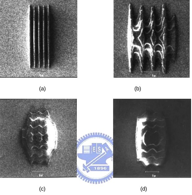
49 Figure 5.3 Variances of Line-Width/Diameter of Wafer CD Bar/Via in Different Types of Reticles Following Continuing 200 hour photo exposure… … … ...50Figure 6.1 I-line symmetrical multiprocessing focus. Pattern length changes observed using an Applied Materials SEM Vision. (a) At focus=0µm, the pattern had the same shape as that on the reticle; (b) at a focus of -0.8µm, the pattern was shortened; (c) at focus=-1.2 µm, the pattern was shortened and completely transformed; (d) at focus=-1.6µm, the pattern irregularly contracted into a shape that resembled an ellipse.… … … .65 Figure 6.2 DUV symmetrical multiprocessing focus. Pattern length changes observed using
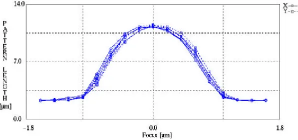
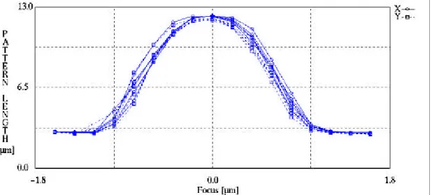
an Applied Materials SEM Vision: (a) At focus=0µm, the pattern had the same shape as that on the reticle, but was longer; (b) at focus=-0.8µm, the pattern was shortened; (c) at focus=-1.2µm, the pattern was shortened and completely transformed; d) at focus=-1.6µm, the pattern became an irregular shapes… ..66 Figure 6.3 Process latitude smiley cur ve of pattern length-focus, with an I-line stepper and a
positive resist… … … ...67 Figure 6.4 The process latitude smiley curve pattern length-focus, with a DUV stepper and
a positive resist. … … … .68 Figure 6.5 I-line light source, PFI-58 resist, exposure dose =200 2
/ cm
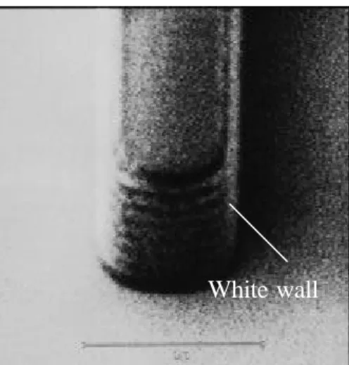
mJ , focus=0µm: Observed with the Applied Materials SEM at a scanning angle of +45°: line-width=0.682 µm, white wall, and three -dimensional picture… … … … .69 Figure 6.6 I-line light source, PFI 58 Resist, Exposure =200 2
/ cm
mJ ; Figures of white wall and Independent Proximity When (a) Focus=+0.4 μm, (b) Focus=-0.4 μm,
E
under multiplying rate 50KV of HITACHI S-9200 CD SEM and Line-Width=0.2μ m. No matter it is ≦0μm or ≧0μm, there is regular triangle while wall… … 70
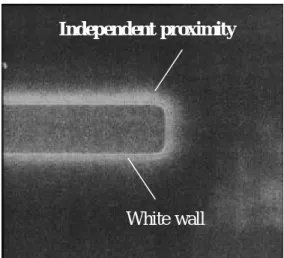
Figure 6.7 Deep UV light source, Exposure =30 2
/ cm
mJ , Figures of white wall and Independent Proximity When Focus=0, under multiplying rate 50KV of HITACHI S-9200 CD SEM and Line-Width=0.2μm. The independent proximity of Deep
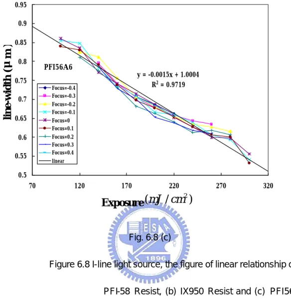
UV is smaller than I-line. … … … ..71 Figure 6.8 I-line light source, the figure of linear relationship of (a) PFI-58 Resist, (b) IX950
Resist and (c) PFI56A6 Resist Exposure- Line Width… … … ..72 Figure 7.1 (a) Stepper Exposure Diagram, (b) Influence of Focus on Exposure Area. (c) Focus Locations following Reflectance and Refraction on Photo Resist and Wafer Surface by Light Source. … … … ...89 Figure 7.2 (a) SEPR 451, (b) SEPR-432 and (c) SEPR-450H, correlation diagram of
exposure dose and line width, (d) Graphs showing exposure dose vs. white wall for three different PR. … … … ...91 Figure 7.3 DUV light source, SEPR 451 photo resist, exposure time =40 2
/ cm
mJ ,
focus=0µm. Observed with the Hitachi SEM at a magnification voltage of 50Kv. i) line-width, ii) white wall. … … … ...95 Figure 7.4 DUV light source, SEPR 432 photo resist, exposure dose =30 2
/ cm
mJ ,
Observed with the Applied Materials SEM at a scanning angle of +45°: (a)
Figure 7.5 Collapse of CD bar for SEPR 451 PR at exposure dose of 80 2
cm
mJ , picture
taken by Applied Materials SEM Vision. … … … ....96 Figure 7.6 Exposure dose becomes too low (10 2
cm
mJ ) for SEPR-450H PR, observed
with the Hitachi SEM at a magnification voltage of 100Kv. PR would not form a pattern… … … ...97 Figure 7.7 (a) high exposure dose (50 2
cm
mJ ) makes CD bar become smaller. (b)Instability of CD bar caused by high exposure dose (60 2
cm
mJ ) for
SEPR-432 PR, by Applied Materials SEM Vision. … … … ..… … ...99 Figure 7.8 (a) add top ARC to SEPR 432, (b) add bottom ARC to SEPR 432, (c) SEPR 432 without adding any ARC, graphs showing standing wave as side wall of CD bar was observed via Applied Materials SEM Vision… … … ..100 Figure 8.1 Stepper Exposure Diagram, Best Focus Locations following Refraction on Photo
Resist and Wafer Surface by Auto Focus Light Source… … … 114 Figure 8.2 Pattern Length Focus Process Latitude Smiley Curve Obtained by Deep UV
Together with SEPR 432 Photo Resist from Wafers Made using (a) fused silica, (b) ALOxNy or (c) TiSixNy via Matrix Exposure… … … ..115
Figure 8.3 Observed with the Applied Materials SEM at a scanning angle of +45°,(a) Fused silica wafer Exposure Dose=46 2
cm
mJ and focus=0.0µm, (b) ALOxNy wafer
Exposure Dose=56 2
cm
mJ and focus=-0.45µm (c) TiSixNy wafer Exposure
Dose=56 2
cm
G
Figure 8.4 Collapse of CD bar for (a) ALOxNy wafer at exposure dose of 56
2
cm
mJ and
focus=-0.65µm (b) TiSixNy wafer at exposure dose of 56
2
cm
mJ and
Chapter 1 Introduction
The fabrication of various solid state devices requires the use of planar substrates, or semiconductor wafers, on which integrated circuits are fabricated. The final number, or yield, of functional integrated circuits on a wafer at the end of the IC fabrication process is of utmost importance to semiconductor manufacturers, and increasing the yield of circuits on the wafer is the main goal of semiconductor fabrication. After packaging, the circuits on the wafers are tested, wherein non-functional dies are marked using an inking process and the functional dies on the wafer are separated and sold. IC fabricators increase the yield of dies on a wafer by exploiting economies of scale. Over 1000 dies may be formed on a single wafer which measures from six to twelve inches in diameter.
The issue of how to transfer a pattern onto a wafer during photolithography is very important. Normally, the resist is treated as a pattern-transferring medium. Such a medium should have a very smooth surface to reduce the focus error. In this experiment, spin coating is used. The velocity of the center differs from that of the outer edges of a rotating disk, so a perfectly smooth surface cannot be obtained. Therefore, resist temperature, cooling
2
temperature, heating temperature, cup temperature, cup humidity and exhaust pressure were controlled to eliminate this imperfection to yield an acceptable error. A lower cooling temperature yields a thicker center, such that the surface of the wafer protrudes at the center. A lower cooling temperature also corresponds to a thicker center, with the same effect. The cup temperature was set to the cooling temperature so that thickness distribution would be the same as. A higher heating temperature yields a thinner photo resist. Higher the humidity yields a thinner photo resist.
Resist is a pho to-sensitive material. If exposed to common white light, a chemical reaction occurs and photolithography cannot be performed. The photolithography process is like the development of a photographic film in that it must be performed in a darkroom. The photolithographic process is further limited since a yellow light source does not promote the resist to react chemically. Accordingly, photolithography should be performed in an environment with a yellow light source. The commonly used light sources in the stepper include the G-line, the I-line and DUV (deep ultraviolet). The G-line wavelength is ~436nm, the I-line ?=350~450nm, and DUV ?=100~300nm. The wavelength of the I-line changes according to the internal composition and gas pressure of the mercury arc lamp used, varying within 350~450nm. This study
employs a superior UV lamp produced by Ushio Inc., which has a ? of 350nm. DUV wavelengths differ according to the laser gas composition: KrF ?=248nm, ArF ?=193nm and F2 ?=157nm. In this work , the DUV stepper’s laser light
source, KrF ?=248nm , was used.
Photolithographic experiments depend on several kinds of measurement instruments. Moreover, the optical process involved is complex. The main aim is to reduce the line-width and make the CD bar even more stable, which is usually achieved by changing the light source. This research seeks to achieve the same results without changing the light source . One method of improvement involves the reticle’s zoom ratio. However, a difference between the reticle’s zoom ratio and this is too large will cause the photolithographic process not to be ideal. In these experiments, the compression ratio applied to the pattern on the reticle and the wafer was 5:1. The compression ratio applied to the DUV was the same as for the I-line.
4 Chapter 2
paper review
Recently, interest in the research and applications of diamond has increased significantly due to the development of the Chemical Vapor Deposition (CVD) technique for producing diamond films. Since diamond has the highest thermal conductivity of all known substances, it has numerous potential applications. However, this high thermal conductivity creates a problem in measuring the thermal conductivity of diamond materials 1,2 . Numerous techniques exist for measuring the thermal conductivity of solid materials3~6. This study proposes a two layer model based on the principle of heat diffusion to determine the thermal conductivity for various CVD diamond thin films based on the effective thermal diffusivity of a diamond film on a silicon substrate measured by using a holographic interferometric technique7. The main sources of distortion for soft pellicle systems include temperature changes and the attachment of curved frames to non-flat reticles, with the latter being the inevitable consequence of the stressed chrome pattern8,9. According to the research by A. Mikkelson in 200110, the reticle oxide layer thickness may reach 20nm, adding 5nm to the wafer, if optical reducing ratio is used.
Wafer throughput in micro-lithography depends on the sensitivity of the resist film to radiation. A lower exposure time required to produce a latent Image in the resist corresponds to a higher throughput11. The focus affects line-width: a focus of 0μm yields the lowest line-width, the width increases
with the focus distance. Positive and negative foci yield symmetrical results12. The primary factor that dominates the gradient of the exposure/line-width relationship is the resist’s internal chemical composition13.
Resist spin coating has been successfully modeled using a detailed non-Newtonian analysis, which allows local fluid viscosity to vary with concentration and shear rate14. The cleavage of a butylester is acid-catalyzed and yields carboxcylic acid and isobutene after exposure to the PAC (Photo Active Component) and PEB (Post-Exposure Back)15. When an acid generator is present in a CAMP (Chemically Amplified) resist formulation, the mechanism for producing a lithographic pattern is simple. The strong acid formed causes deprotection at a relatively low temperature with an activation energy of around 11 to 14 kcal/mol16.
Wafer throughput in micro-lithography depends on the sensitivity of the resist film to radiation. A lower exposure time required to produce a latent Image in the resist corresponds to a higher throughput17 . The designed by
6
Watanabe et al.18 showed that the focus margin for 0.3µm lithography with a KrF excimer stepper is ±0.08µm for DOF (Depth of Focus) of ±0.5µm. It is possible for an ArF excimer laser stepper to achieve 0.13µm lithography with a DOF of ±0.5µm by using the recently developed technique of super resolution. The wafer surface profile is structure of the device and has irregularities of 0.3 to 1µm. As optical lithography will not reach the necessary resolution for future demands in microengineering. Now lithographic techniques have to be ready to produce nanostructures in a parallel way. Atoms with thermal kinetic energies have de Broglie wavelengths in the picometer regime and so they do not suffer from diffraction when focused down to a nanometer scale spot size. In the last decade the investigation of atom light interaction has shown, that the trajectories of neutral atoms can be efficiently manipulated with laser light and that optical elements for neutral atoms can be built using the resonant interaction with laser light 18 −21 .
Chapter 3
The traditional reticle level detects the method
Introduction
In an apparatus for monitoring any deviation of a planar surface from its desired position, a light source and a light detector are positioned so that when the surface is at the desired position a beam of light projected by the light source is reflected by the surface and fully registers on the light detector causing the light detector to generate a peak output signal. When the surface deviates from its desired position, the reflected beam of light does not fully register on the light detector, causing the light detector to generate less than peak output signal.
Summary of the reticle level detects the method
According to an embodiment of the present invention, depicted in Figure 3.1 is an optical level detector configured for monitoring whether a planar surface has deviated from its desired position, represented by a reference plane. Reference plane only represents a desired position for the planar surface and does not represent a physical surface. Optical level detector is
8
positioned at a known distance X from the reference plane . The absolute value of the distance X is not important but it is important that the distance X
be fixed and does not change once the optical level detector is set up.
Associated with the reference plane is an incidence axis and a reflection axis . The incidence axis represents the path of an incident light beam from a light source incident to the reference plane and defines a refe rence incidence angle ?1 between the reference plane and the incidence axis. When a planar
surface is placed at the reference plane, the incidence beam will be reflected by the planar surface and returned towards the optical level detector as a reflected beam. The reference reflection axis represents the path of the reflected light beam when the planar surface is placed at the position defined by the reference plane, i.e. the desired position for the planar surface. The reference reflection axis defines a reference reflection angle ?2, which is equal to the incidence angle ?1, between the reference plane and the reference reflection axis. Therefore, by positioning a light detector in line with the
reference reflection axis, one may detect whether the planar surface has deviated from the reference plane.
In the embodiment of the present invention illustrated in Figure 3.1, the light source is provided in the optical level detector for projecting a narrow beam of
light, the incidence beam, on to the planar surface. The light source is preferably a laser or a light emitting diode but any other light source may be adopted for this purpose. The light source projects the incidence beam along its projection axis. In this embodiment of the present invention, the light
source is positioned such that the projection axis is coincident with the incidence axis. Thus, the incidence beam propagates along the path defined by the incidence axis and on to the planar surface. The incidence beam is reflected by the planar surface and travels back to the optical level detector as a reflected beam. The optical level detector is provided with a light detector for receiving this reflected beam.
The light detector is positioned with its viewing axis coincident with the reference reflection axis so that when the planar surface is in its desired position, the reflected light beam falls squarely on the light detector. The light detector is preferably a device such as a photocell that converts the light energy of the reflected beam into an electrical signal that can be readily detected and monitored. The voltage level of a typical photocell’s output signal will vary proportionally with the intensity or the amount of light shone on the photocell. Thus, when the reflected beam falls completely on the light detector (i.e. fully registers with the light detector), the output signal of the light detector
10
will be at the peak voltage value possible with the reflected beam. If the reflected beam falls on the light detector only partially (i.e. does not fully register with the light detector), the output signal of the light detector will be at some voltage value less than the peak value.
This ensures that when a planar surface is in its desired position, i.e. at the position represented by the reference plane, the reflected beam will be coincident with the viewing axis and the reflected beam will completely register with the light detector. In this scenario, the output signal of the light detector will exhibit a peak voltage value for the given planar surface and its light reflecting characteristics. It should be noted that the peak voltage value of the light detector in this context does not necessarily mean the absolute peak voltage value that the light detector is capable of producing. It refers to the peak voltage value that the light detector will produce in the given configuration of the optical level detector.
If the planar surface deviates from its desired position, the reflected beam will not be coincident with the reflection axis and, in turn, not coincident with the viewing axis of the light detector. Thus the reflected beam will not completely register with the light detector. Depending on the degree of the deviation, the reflected beam could completely miss the light detector or only
partially register with the light detector. In either case, the resulting output signal of the light detector will exhibit a voltage value that is less than the peak value.
The exemplary configuration of Figure 3.1 represents the situation where the planar surface is in its desired position. Thus, the angle of incidence for the incidence beam with respect to the planar surface is same as the reference incidence angle ?1. And, correspondingly, the angle of reflection for the
reflected beam with respect to the planar surface is same as the reference reflection angle ?2.
Thus, the optical level detector of the present invention can be used to determine whether a planar surface has deviated from its desired position, represented by the reference plane by monitoring the output signal of the light detector. The output signal can be monitored using any suitable circuits or devices that can measure the voltage level of the output signal. Such circuits or devices are well known to one of ordinary skill in the field and they need not be discussed in detail here. Figures 3.2 and 3.3 illustrate some examples of a number of different situations in which a planar surface may deviate from the reference plane which can be detected by the optical level detector.
12
In Figure 3.2, the planar surface has deviated from the reference plane by an angular translation represented by angle ß . The incidence beam will strike the planar surface at a n incidence angle a1 and the reflected beam leaves the planar surface at a reflected angle a2. As illustrated, the resulting reflected
beam also has been angularly translated from the viewing axis of the light detector by the angle ß . The reflected beam is not coincident with the viewing
axis and no longer registers with the light detector. The resulting output signal of the light detector will be zero volts, signifying that the planar surface has deviated from the reference plane. If the translation angle ß is sufficiently
small, the reflected beam may register partially with the light detector. The output signal of the light detector, then, will not be zero volts but it will be something less than the peak value, still signifying that the planar surface has deviated from the reference plane.
In Figure 3.3, the planar surface has deviated from the reference plane by a linear translation represented by Y. The incidence beam will strike the planar surface at an incidence angle a1 and the reflected beam leaves the planar surface at a reflected angle a2. The planar surface is parallel to the reference plane and the incidence angle a1 and the reflected angle a2 are same as the reference incidence angle ?1 and the reference reflected angle ?2,
respectively. However, the reflected beam will be translated accordingly as represented by Y’ and thus the reflected beam will not be coincident with the
viewing axis of the light detector. Again, the reflected beam will not fully register with the light detector and the outp ut signal of the light detector will be some value less than the peak value, signifying that the planar surface has deviated from the reference plane.
In another embodiment of the present invention, the light source and the light detector may be mounted in the optical level detector such that they are not coincident with the projection axis and the viewing axis, respectively, to accommodate different mounting configurations. For example, in Figure 3.4, the light source and the light detector are mounted in horizontal configuration, but by employing reflectors and respectively, the incidence beam and the reflected beam are made to travel along the desired paths. The reflectors may be mirrors, prisms or other suitable reflectors. The light source and the light detector may be configured in many different orientations as long as the reflectors are used to direct the incidence beam and the reflected beam to propagate along the desired paths.
In certain applications, a plurality of the optical level detector may be utilized to monitor positions of a plurality of surface regions on a planar surface.
14
For example, as illustrated in Figure 3.5, a planar surface may have a surface region A that is on the reference plane but the remainder of the planar surface represented by surface region B may be deviated from the reference plane. If one optical level detector was monitoring the surface region A, the planar
surface may seem as though it is on the reference plane. Thus, two or more optical level detectors may be utilized to monitor a plurality of surface regions on the planar surface to better detect any deviations from the reference plane. The inventor has applied the optical level detector of the present invention in such a manner in detecting out-of-level reticles (or photo lithographic masks) during the photolithography processes in semiconductor wafer manufacturing.
In one application, illustrated in Figure 3.6, four optical level detectors similar to the embodiments described herein may be mounted on a reticle stage of a stepper tool. The reticle stage has a reticle holding well for holding a reticle in place. Each of the four optical level detectors may be positioned near each of the four corners of the reticle holding well, as identified by the reference numbers. The optical level detectors are used to monitor whether
or not a reticle (not shown) placed on the reticle holding well is properly leveled. Each of the four optical level detectors may be configured, for example, so that their light detectors generate peak output signal values when the reticle is
properly leveled in the reticle holding well. The output signals of the light detectors may be monitored individually. Alternatively, the optical level detectors may be connected in series and monitor the total voltage of the output signals.
Figure 3.7 illustrates a sectional view of an optical level detector as implemented by the inventor on the reticle stage according to another embodiment of the present invention. The light source is attached to the optical level detector by a light source holding plate. The light from the light source passes through a pin hole in the optical level detector and emerges as the incidence beam. The incidence beam is reflected by the planar surface (representing a reticle surface) and if the planar surface does not deviate from the reference plane, the reflected beam will be coincident with the reference reflection axis. In this example, the light detector is positioned in the optical level detector in a configuration similar to that discussed in reference to Figure 3.4. The light detector is provided such that its viewing axis is horizontally oriented and not coincident with the reference reflection axis. A reflector is provided at an appropriate orientation so that when the planar surface is at the desired location and does not deviate from the reference plane, the reflected beam will be deflected towards the light detector and fully register with the light
16
detector through the hole provided in the optical level detector. As with the other embodiments of the present invention discussed herein, when the planar surface deviates from the reference plane, the reflected beam will no longer be in proper alignment with the reference reflection axis and the reflected beam will no t fully register with the light detector. By monitoring the electrical output signal of the light detector, one can thus detect whether or not the planar surface is at the desired location represented by the reference plane.
In the particular configuration implemented by the inventor, the optical level detector is mounted on to the reticle stage by a set of connecting hardware that allows the height of the optical level detector to be adjusted relative to the reticle surface (the planar surface). The set of connecting hardware comprises a vertically actuating guide bearing that allows the height of the optical level detector to be adjusted and an L-bracket for attaching the whole assembly on to the reticle stage. The guide bearing is a standard slide/bed type comprising a slide and a bed. To adjust and control the height of the optical level detector attached to the guide bearing, a worm gearing set up is used. The slide is provided with wormgear teeth and a worm is situated in the bed. The worm has a thumb screw to enable a human operator to adjust the height of the optical level detector buy turning the thumb screw. These connecting hardware may
be viewed in more detail in the exploded view of the assembly illustrated in Figure 3.8. As discussed in reference to Figure 3.6, four of the optical level detector may be installed near the four corners of the reticle holding well using the connecting hardware described herein to verify that the reticle is properly leveled in the reticle holding well before the stepper is operated. The vertically actuating guide bearing may be of other types of guide bearing well known in the art and not necessarily limited to the slide/bed type described herein.
The use of the optical level detector of the present invention has simplified the stepper tool operator's task of verifying that the reticle is properly level in the reticle stage. While the foregoing invention has been described with reference to the above embodiments, various modifications and changes can be made witho ut departing from the spirit of the invention. Accordingly, all such modifications and changes are considered to be within the scope of the appended claims.
26 Chapter 4
The traditional thermal of slightly out of shape reticle detects the method Introduction
The present invention relates to reticles used in the formation of integrated circuit (IC) patterns or dies on semiconductor wafer substrates. More particula rly, the present invention relates to a thermal detector which determines whether a reticle is thermally distorted to an excessive degree prior to exposure of a wafer through the reticle in photolithography.
Summary of the reticle thermal detects the method
The present invention contemplates a novel reticle thermal detector which is suitable for determining whether a reticle is distorted typically due to thermal effects from an exposure light source in a stepper or scanner prior to exposure of a semiconductor wafer through the reticle. The reticle thermal detector alerts personnel to the distorted condition of a reticle as the reticle lies on a reticle stage in a stepper or scanner preparatory to a photolithography process. Therefore, the distorted reticle can be removed and a replacement reticle placed on the reticle stage to ensure that a circuit pattern of high integrity is transmitted from the reticle to a wafer with precision during photolithography.
In one embodiment, the reticle thermal detector of the present invention is an optical reticle thermal detector and includes a transmitter such as a laser beam transmitter or a light-emitting diode, for example. A receiver is positioned in spaced-apart relationship with respect to the transmitter, with the transmitter and receiver located on opposite sides of a reticle stage in a stepper or scanner. An alarm connected to the receiver receives an activation signal from the receiver when the receiver fails to receive a beam reflected from the reticle. Prior to exposure of a wafer through a reticle placed on the reticle stage, the transmitter emits a light or infrared beam which is reflected from the surface of the reticle and into the receiver as catoptric energy. As long as the reticle is in an undistorted configuration, the beam is reflected from the reticle at such an angle that the reflected beam enters the receiver and the alarm is not activated. On the other hand, in the event that the reticle is thermally distorted, the distorted reticle deflects the reflected beam from entering the receiver. The receiver, in turn, activates the alarm and thereby alerts personnel to the thermally-distorted condition of the reticle.
In another embodiment, the reticle thermal detector includes a mechanical device which determines whether the reticle is thermally distorted through mechanical means. In the event that the reticle is distorted, the mechanical
28
device activates the alarm. In still another embodiment, the reticle thermal detector includes an electromechanical device which determines whether the reticle is distorted and activates the alarm in the event that the reticle is distorted. The invention further includes a novel method of enhancing the quality of circuit pattern images formed on a wafer during photolithography by monitoring the distorted state or configuration of a reticle prior to use of the reticle in photolithography.
In still another embodiment, the invention includes an exposure apparatus such as a scanner or stepper which includes a reticle thermal detector. The exposure apparatus includes an exposure device for exposing a wafer. The exposure device includes a light source for emitting light, a reticle stage adjacent to the light source for holding a reticle and a lens adjacent to the reticle stage. The reticle thermal detector includes a mechanism for determining a degree of distortion of the reticle provided adjacent to the reticle stage and an alarm connected to the mechanism for activation by the mechanism when the reticle is distorted.
Referri ng initially to Figures 4.1-4.3, an illustrative embodiment of an optical reticle thermal detector of the present invention is generally indicated by reference numeral. The optical reticle thermal detector is designed to be
installed in a stepper or scanner which may be conventional and is used to transmit circuit pattern images from a reticle to a semiconductor wafer substrate (not shown) in the photolithography step of semiconductor fabrication. The stepper/scanner includes a reticle stage for holding the reticle; a lens beneath the reticle stage; and a positive focal point, a center focal point and a negative focal point beneath the lens. A light source is disposed above the wafer stage for emitting light through the reticle.
During photolithography, a semiconductor wafer (not shown) is placed on a wafer stage (not shown) at the center focal point. Light is emitted from the light source through the reticle and lens, respectively. When the reticle is in an undistorted configuration, the lens focuses the circuit pattern image defined by the reticle onto the wafer at the center focal point. This results in a circuit pattern of high integrity and quality being formed on the wafer.
On the other hand, throughout extended use, the light from the light source tends to heat the reticle, thus causing the reticle to expand and become thermally distorted. This, in turn, causes the circuit pattern image to become focused above the center focal point (toward the positive focal point) or below the center focal point (toward the negative focal point). Consequently, the circuit pattern image transmitted to the wafer at the center focal point becomes
30
distorted, resulting in a distorted circuit pattern image of low quality being formed on the wafer.
The optical reticle thermal detector of the present invention includes a transmitter and a receiver which are disposed in spaced-apart relationship with respect to each other on opposite sides of the reticle stage. A computer is connected to the light receiver, typically through computer wiring. An alarm is, in turn, connected to the computer typically through alarm wiring. The transmitter and receiver are positioned in such a manner that an incident beam emitted from the transmitter is reflected from the reticle as a reflected beam which enters the receiver as catoptric energy when the reticle is in an undistorted configuration.
The transmitter may be any light-emitting element known by those skilled in the art, including but not limited to a laser-emitting device or an LED (light-emitting diode), for example. Alternatively, the transmitter may be any device which is suitable for emitting a beam of electromagnetic radiation such as infrared radiation, for example. The receiver may be any device which is capable of receiving a reflected light or radiation beam and responsively transmitting an electrical signal to the computer (or alternatively, transmitting a modulated electrical signal or terminating transmission of an electrical signal to
the computer) in the event that the reflected light or radiation beam is no longer received by the receiver. The alarm may be an audible alarm, a visual alarm, or both an audible and visual alarm. The computer is programmed to activate the alarm in the event that the receiver transmits an electrical signal to the computer, transmits a modulated electrical signal to the computer or terminates transmission of an electrical signal to the computer.
In operation of the optical reticle thermal detector, a reticle is initially placed in the reticle stage of the stepper/scanner, and a semiconductor wafer (not shown) having a photoresist layer deposited thereon is placed on a wafer stage (not shown) in the stepper/scanner. Under circumstances in which the reticle is generally in thermal equilibrium with the environment (such as may occur, for example, upon initial placement of a previously unused reticle in the reticle stage), the reticle is in an undistorted condition, as illustrated by the area bounded by the solid lines and indicated by refe rence numeral in Figure 4.2. Therefore, the reticle is suitable to transmit a circuit pattern image of high quality onto the wafer (not shown) placed on the wafer stage in the stepper/scanner during a subsequent photolithography process. On the other hand, under circumstances in which the reticle has been heated to an excessive degree, typically by the light from the light source (such as may
32
occur throughout prolonged usage of the reticle in the stepper/scanner), the reticle is in an expanded, thermally-distorted configuration, as illustrated by the area bounded by the dashed lines and indicated by reference numeral in Figure 4.2. Therefore, the distorted reticle is not suitable to transmit a high-quality circuit pattern image onto the wafer during a subsequent photolithography process.
Prior to the photolithography process, the thermal state of the reticle is determined by the reticle thermal detector. Accordingly, an incident light or radiation beam is emitted from the transmitter, typically against the upper surface of the reticle. Figure 4.1 illustrates the case in which the reticle is in an undistorted configuration. In that case, a reflected beam is reflected from the reticle and enters the receiver as catoptric energy. As long as the reflected beam enters the receiver, the receiver does not transmit an electrical signal to the computer through the computer wiring. Therefore, the computer refrains from activating the alarm through the alarm wiring and the photolithography process can proceed.
During photolithography, light is emitted from the light source and through the reticle and lens, respectively. The lens focuses the light, in the form of the circuit pattern image in the reticle, onto the wafer (not shown) located at the
center focal point. Due to the undistorted configuration of the reticle, the circuit pattern image transmitted to the wafer has a high resolution and facilitates the etching of high-quality circuits on the wafer during subsequent process steps.
In the event that the reticle has been heated excessively (such as by the heat source after prolonged use in the stepper/scanner, for example), the reticle becomes thermally distorted. This is indicated by the dashed lines in Figure 4.2, in which the enlarged area of the reticle indicated by reference numeral represents the increased size of the distorted reticle relative to the normal, undistorted size (indicated by reference numeral). Consequently, as shown in Figure 4.3, the distorted reticle deflects the reflected light beam away from entering the receiver. Therefore, the receiver transmits an electrical signal to the computer, through the computer wiring. Responsive to the signal from the receiver, the computer transmits an alarm activation signal to the alarm, through the alarm wiring. The alarm broadcasts an audible signal, a visual signal or both an audible and a visual signal to alert personnel to the distorted condition of the reticle. Therefore, the reticle can be removed from the reticle stage and replaced with an undistorted reticle to ensure transmittal of a high-quality circuit pattern image from the reticle onto the semiconductor wafer.
34
In the configuration of the reticle thermal detector heretofore described, the receiver transmits an electrical signal to the computer 16 and the computer activates the alarm in the event that the reflected beam does not enter the receiver. However, it is understood that alternative operational configurations are possible. For example, the receiver may be adapted to transmit an electrical signal to the computer under circumstances in which the reticle is undistorted (and the reflected beam therefore enters the receiver). In that case, the receiver does not transmit the signal to the computer and the computer consequently activates the alarm if the reflected beam does not enter the receiver (thus indicating that the reticle is distorted). In another alternative configuration, when the reticle is undistorted, the receiver transmits a baseline signal to the computer as long as the reflected beam enters the receiver. If the reticle is distorted, the receiver transmits a modulated electrical signal to the computer, which activates the alarm responsive to receiving the modulated signal from the receiver.
Referring next to Figure 4.4, a mechanical retical thermal detector according to the present invention is generally indicated by reference numeral. The mechanical retical thermal detector includes a mechanical device which engages a reticle when the reticle rests on a reticle stage of a stepper/scanner
(Figure 4.1). A computer is connected to the mechanical device typically through computer wiring. An alarm, which may be an audible alarm, a visual alarm or both, is connected to the computer typically through alarm wiring. The mechanical device may be any device which is capable of detecting an abnormal thickness of the reticle when the reticle is in a thermally distorted configuration and transmitting an electrical signal (or alternatively, transmitting a modulated electrical signal or terminating transmission of the signal) to the computer in the event that the reticle is distorted. Accordingly, in the event that the reticle is undistorted, the computer does not activate the alarm. In the event that the reticle is distorted, the mechanical device causes the computer to activate the alarm by transmitting an electrical signal, transmitting a modified electrical signal or terminating transmission of an electrical signal to the computer. The reticle can then be replaced by an undistorted reticle prior to photolithography.
Referring next to Figure 4.5, an electromechanical retical thermal detector according to the present invention is generally indicated by reference numeral. The electromechanical retical thermal detector includes at least one, and typically, multiple piezoelectric sensors which engage a reticle when the reticle rests on a reticle stage of a stepper/scanner (Figure 4.1). A computer is
36
connected to the piezoelectric sensors typically through computer wiring. An alarm, which may be an audible alarm, a visual alarm or both, is connected to the computer typically through alarm wiring. The piezoelectric sensors are capable of sensing pressure exerted by the reticle when the reticle is in an expanded, thermally distorted configuration, in which case the piezoelectric sensors generate and transmit an electrical signal to the computer through the computer wiring. Consequently, the computer activates the alarm through the alarm wiring. In the event that it is undistorted, the reticle does not exert pressure on the sensors. Consequently, the sensors do not transmit an electrical signal to the computer and the computer does not activate the alarm. While the preferred embodiments of the invention have been described above, it will be recognized and understood that modifications can be made in the invention and the appended claims are intended to cover all such modifications which may fall within the spirit and scope of the invention.
40 Chapter 5
Improvement in instable analysis of heat inflation induced line-width after replacing pellicle with diamond film on reticle (photo-masks)
Introduction
Recently, interest in the research and applications of diamond has increased significantly due to the development of the Chemical Vapor Deposition (CVD) technique for producing diamond films. Since diamond has the highest thermal conductivity of all known substances, it has numerous potential applications. However, this high thermal conductivity creates a problem in measuring the thermal conductivity of diamond materials 1,2 . Numerous techniques exist for measuring the thermal conductivity of solid materials3~6. This study proposes a two layer model based on the principle of heat diffusion to determine the thermal conductivity for various CVD diamond thin films based on the effective thermal diffusivity of a diamond film on a silicon substrate measured using a holographic interferometric technique7. The main sources of distortion for soft pellicle systems include temperature changes and the attachment of curved frames to non-flat reticles, with the latter being the inevitable consequence of the stressed chrome pattern8,9.
The heat conduction equation
For one dimensional heat flow along the y direction, the rate change of heat transfer can be expressed as
dy dT A k dt dQ s − = (1)
where k denotes the thermal conductivity along the y direction in the unit s
of Wm−1 K−1, dT dy represents the temperature distribution along the y direction of K m−1, A is the cross sectional area of the sample perpendicular to the heat transfer direction of 2
m , and dQ dt denotes the thermal power of W. Notably, thermal conductivity, k , is a heat transfer value per unit temperature s
gradient per unit time through unit cross section, which is perpendicular to the heat transfer direction. The temperature gradient through the unit cross section then can be measured by introducing a known quantity of heat to the solid material to determine the value of ky from Eqn. (1).
Modeling of thermal conductivity in a solid begins with the diffusion equation: ) , , , ( 1 1 2 t z y x Q k t T T s − = ∂ ∂ − ∇ α (2)
When α denotes the thermal diffusivity, for a long, thin film of a
homogeneous material, with one end of the thin film held at a constant temperature and the other end heated at a known rate, the steady state, one dimensional temperature distribution is determined by the familiar expression
42
from Eqn. (2).
Fourier’s law, Eqn. (1), can be used to determine the conduction heat transfer rate. That is,
) ( material,1 material,2 y T T L kA dy dT kA q =− = − (3)
Particularly, an analogy exists between heat diffusion and electrical charge. Just as an electrical is associated with the conduction of electricity, a thermal resistance may be associated with the conduction of heat. Defining resistance as the ratio of a driving potential to the corresponding transfer rate, Eqn. 3 shows that the thermal resistance for conduction is
kA L q T T R y material mateial − = ≡ ,1 ,2 (4)
Comparisons between traditional pellicle-reticle model and diamond films-reticle thermal conductivity model
Equivalent thermal circuits may also be used for more complex systems, such as composite walls. Such walls may involve numerous series and parallel thermal resistances due to layers of different materials. Consider the series composite wall of Fig. 5.1 (a) and (b). The one dimensional heat transfer rate for this system can be expressed as
(5)
Consider the traditional pellicle-reticle of a two-layer composite, as illustrated in Fig. 5.1 (a) Each layer is characterized by an individual thickness, y density, heat capacity, and thermal conductivity, k. where T1−T3is the overall
temperature difference and the summation includes all thermal resistances. Consequently, ) ( 3 1 A k L A k L T T q chromiuml chromium quartz quartz y + − = (6)
Alternatively, the heat transfer rate can be related to the temperature difference and resistance associated with each element.
A k L T T A k L T T q chromium chromium quartz quartz y 3 2 2 1 ) ( − = − = (7)
Consider the diamond film-reticle thermal resistances of a three-layer composite, as shown in Fig. 5.1 (b),
) ( ' 4 ' 1 ' A k L A k L A k L T T q diomond diomond chromiuml chromium quartz quartz y + + − = (8)
Alternatively, the heat transfer rate can be related to the temperature difference and resistance associated with each element.
∑
− = R T T q n y 144 A k L T T A k L T T A k L T T q doomond diomond chromium chromium quartz quartz y ' 4 ' 3 ' 3 ' 2 ' 2 1 ' ' ) ( − = − = − = (9)
The initial temperature is the same for the traditional pellicle-reticle and diamond-reticle, so T1 =T1'. However, due to the effects of the thermal conductivity of diamond film, T2 ≠T2',T3 ≠T3'. Putting Table 1 into Eqns. 7 and
9 demonstrates that a diamond film-reticle has better heat radiation.
Experimental method
A 10μm thick layer of diamond film(TypeⅡa) is deposited on a chromium
layer on the bottom of a reticle via CVD using Cymer KrF Laser as the source of photo exposure. Figure 5.2 describes the laser route in which the Cymer machine shoots a highly homogeneous light that could control uniformity below 0.3% via a fly eye. The homogeneous laser light obtains zero order and 1st order light via annular aperture. The laser beam of zero order and 1st order light could be controlled under experimental size following going through a reticle blind. Subsequently, through the main condenser lens, the main condenser lens is the final optical element for the exposure beam before
entering the reticle and reduction projection, the condenser lens to ensure beam telecentricity. The final lens is the projection lens. The main function of the projection lens is to reduce the laser ratio to 4:1 and project it onto the wafer surface.
Results
Diamond Reticle thermal conductivity
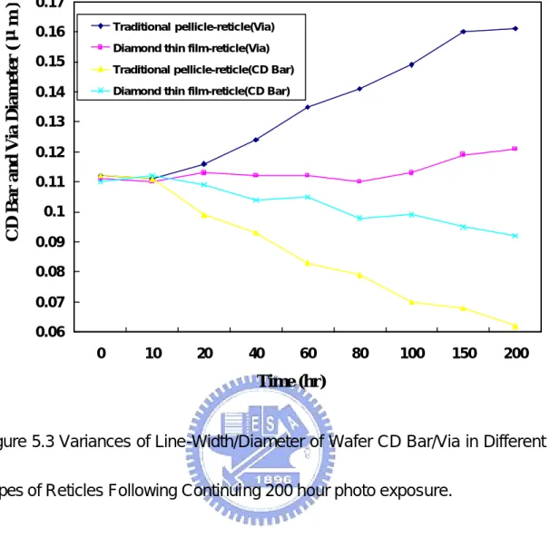
When the reticle receives extended light energy, it will be out of shape due to thermal inflation. The CD (Critical Dimension) Bar from coating positive resist on the wafer of inflated reticle thus will shrink. Figure 5.3 may prove that traditional pellicle-reticle is four times the quantity of out–of-shape than diamond thin film under continuing photo exposure for 200 hours. At this point, the temperature of the traditional pellicle -reticle increases from 23.01℃ to 24.34℃ while the temperature of the diamond thin film reticle increases from 23.00℃ to 23.03℃. The increase of 1.33℃ reduces the CD bar by 0.05μm.
46
of CD Bar can be obtained. Figure 5.3 shows that the increase of just 0.03℃
has almost no effect on 35nm process. This result demonstrates that diamond is a new and ideal replacement for pellicle in both theory and practice.
Diamond Reticle Intensity
Table 2 shows that the value of measurement of intensity of reticle of quartz and chromium is 227.6 2
/ cm
mW and following adding a layer of pellicle, the value of intensity reduces by 0.483% while the value of intensity of diamond-reticle reduce by 17.97%. The loss of energy after light increase the medium of diamond is the weakness that will make throughput of scanner slow down.
Effects of improved oxide layer on diamond reticle on CD (Critical Dimension) bar
According to the research by A. Mikkelson in 200110, the reticle oxide layer thickness may reach 20nm, adding 5nm to the wafer, if optical reducing
ratio is used. The 35nm via(hole)-process increases the size to 40nm and reduces the CD bar to 30nm.
Because chromium wire of diamond-reticle is wrapped up between diamond and quartz, the chromium does not contact with air, and no oxide phenomenon occurs. The design of diamond -reticle provides a method of preventing reticle from producing an oxide layer.
Conclusions
Today’s photo manufacturing process has not had ability to produce 35nm line-width, so the experiment used 0.11μm manufacturing technology to act
as quantity of transformation of thermal inflation and applied the quantity of transformation to future 35nm manufacturing process.
Presently, the tolerable standard of error of margin of semiconductors is 3 sigma. In the 65nm process, the error of margin 5nm is within 3 sigma while the error margin in 35nm process exceeds 3 sigma. Therefore, when a semiconductor process is developed to 35nm, the slight shape change due to heat must be resolved. However, until now, no paper or patent has offered a solution. Diamond film reticle may provide a solution for achieving slight shape change in the future.
48 List of Table
Table 5.1
Thermal properties of film and substrate [HITAHI PD 5000 Manual]
Material Thickness Thermal conductivity (W /m K )
Quartz 6.30 mm 4.8 Chromium pattern 100 nm 93.7 Pellicle 0.08 mm - CVD Diamond film (TypeⅡa) 10μm 1193 Table 5.2
Various types of reticle intensity
No Pellicle-reticle Pellicle-reticle Diamond film-reticle
Intensity ( 2
/ cm
(a) Traditional reticle
(b) Diamond film reticle Laser light Laser light Quartz Chromium Pattern Pellicle Quartz Chromium Pattern Diamond film 1 T 2 T 3 T ' 1 T ' 2 T ' 3 T ' 4 T
Pellicle Volume (void)
Y X ) (qy ) (qy
Figure 5.1 Route Map of Laser Beam Used in Experiment
Laser beam Fly’s Eye Laser beam Annular Aperture Reticle Blind Main Condenser Lens Reticle Projection Lens Wafer
50 0.06 0.07 0.08 0.09 0.1 0.11 0.12 0.13 0.14 0.15 0.16 0.17 0 10 20 40 60 80 100 150 200 Traditional pellicle-reticle(Via) Diamond thin film-reticle(Via) Traditional pellicle-reticle(CD Bar) Diamond thin film-reticle(CD Bar)
CD Bar and Via Diameter (
μm )
Time (hr)
Figure 5.3 Variances of Line-Width/Diameter of Wafer CD Bar/Via in Different Types of Reticles Following Continuing 200 hour photo exposure.
Chapter 6
Analysis of instability in a Critical Dimension Bar due to focus and exposure
Introduction
In the photolithography processing of semiconductor, line-width is smaller and smaller. Therefore, the requirements of process window are stricter than before. Among them, the control of focus and exposure dose is one of the most important factors that may affect line-width. Bad control of focus and exposure may not only affect line -width, but also cause the increment of rejects of products. The research explored mainly the effects of focus and exposure dose on line -widths of different photo resists. The research obtained related coefficients of exposure dose-line width and focus-line width by coating photo resist of different components on the surface of silica wafer. The results of research found that focus might not only change line-width but also had positive-negative symmetric relationship with line-width. It also found that there was linear relationship between exposure dose and line -width.
52 Experimental
Equipment
The steppers were a Nikon I-line and DUV. The major function of a stepper is to apply the exposure pattern to the surface of a wafer that has already been coated with a layer of resist. The main difference between an I-line stepper and a DUV stepper is that they use different light sources. The light source used by an I-line stepper is a UV lamp ?=365nm, while the light source used by a DUV stepper is a KrF excimer laser ?=248nm. The differences between the wavelengths of these light sources lead to different resolutions. Generally, a shorter wavelength gives a better resolution, and a better resolution enables the line -width to be made narrower.
The exposure field used by the I-line stepper was a 6inch/22mm square of glass material. The LNA (Lens Numerical Aperture)=0.60 and the INA (Input Numerical Aperture)=0.38. The NAs (numerical apertures) were fixed.
The exposure field used by the DUV stepper was a 6inch/22mm square of glass material. LNA=0.60 and INA=0.45. The Nikon stepper has two numerical apertures. The INA is the front-end of the lens through which the arc lamp or
the laser light passes. The INA did no affect the experiment. The LNA is divice of Aperture in Projection LENS. Numerical Aperture in this experiment means LNA. Hence, LNA=NA (s=INA/LNA, I-line and DUV Illumination aperture used conventional types). Generally, the NA of the DUV can be opened wider because the resolution of the resist used with DUV is higher than with the I-line.
For SEM (scanning electron microscopy), the microscopes used were a Hitachi S-9200, a KLA_Tencor 8100, and an Applied Materials’ SEM Vision. The Hitachi S-9200’s primary function was to measure the pattern’s line-width and the capture a top view of the image. The error correction method involved a standard wafer that, after etching, had a line-width of 0.3µm±10%. The line-width of this standard wafer was measured and if the result was within 0.3µm±10%, that was considered to meet our requirements. The error between the results obtained by the KLA_Tencor and those obtained by the Hitachi S-9200 was not allowed to exceed ±10%.
The Applied Materials SEM Vision was not used to measure line -width because its top view measurement was worse than those made with the
54
Hitachi S-9200 or the KLA_Tencor 8100. The Applied Materials SEM Vision was used mainly to view a pattern in three–dimensions. This SEM provides the advantage of having an E-beam that measure the wafer’s surface at ±45° and 0°. This SEM therefore enables a pattern to be observed in three dimensions .
The TEL CLEAN ACT-8 machine was used for spin coating and as a developer. The main functions of the ACT-8 are {1} priming, {2} spin coating, {3} soft baking, and {4} developing
{1} A layer of HMDS (Hexamethyldislazane) (CH3)3SiNHSi(CH3)3 is
sprayed onto the wafer. HMDS functioned as a medium that strengthened the bond between resist and wafer surface. After suitable priming, the wafer surface energy can be adjusted to a level similar to the resist surface energy to increase the adhesive strength between the wafer surface and the resist. {2} After dehydration baking and priming, the liquid resist must be evenly applied to the wafer surface. The resist was dripped onto the center of the wafer and distributed over its surface by the centrifugal force due to high-speed rotation. A higher rotation speed yields a thinner and more uniform resist liquid. The resist includes a very volatile organic solvent. After the resist is sprinkled onto the wafer surface, the stickiness of the resist changes with the volatility of the solvent. Failing to complete the coating before the solvent becomes volatile