國
立
交
通
大
學
電機與控制工程系
碩
士
論
文
單迴路積分三角類比數位轉換器之積分
器充電雜訊與諧波功率模型
Analytical Settling Noise and Distortion Power Models
of Sigma-Delta ADCs
研 究 生:黃俊傑
指導教授:陳福川 教授
單迴路積分三角類比數位轉換器之積分器充電雜訊
與諧波功率模型
Analytical Settling Noise and Distortion Power Models
of Sigma-Delta ADCs
研 究 生:黃俊傑 Student:Chun-Chieh Huang
指導教授:陳福川 Advisor:Fu-Chuang Chen
國 立 交 通 大 學
電 機 與 控 制 工 程 系
碩 士 論 文
A ThesisSubmitted to Department of Electrical and Control Engineering College of Electrical Engineering
National Chiao Tung University in partial Fulfillment of the Requirements
for the Degree of Master
In
Electrical and Control Engineering September 2008
Hsinchu, Taiwan, Republic of China
單迴路積分三角類比數位轉換器之
積分器充電雜訊與諧波功率模型
研究生:黃俊傑 指導教授:陳福川 教授 國立交通大學 電機與控制工程研究所摘要
交換式電容積分器是積分三角轉換器中基本的建構成份。其電容不完全的充 放電轉換特性(積分器充放電問題)為積分三角轉換器中一個主要影響輸出誤差 的來源。而因為積分器充放電問題的高複雜性,相關的誤差和失真的解析模型實 際上是不存在的。在此篇論文中,我們的目的在於經由非線性擬合方法和輸出端 頻譜預測技術來分析積分器充放電問題。由上法,積分器充放電問題誤差和失真 的封閉解可獲得,且可使用積分三角轉換器中的系統參數來組成函數以呈獻出 來。同時我們使用了行為層的模擬以及HSPICE 電路的模擬來驗證此解析模型的 正確性,驗證結果顯示出我們的解析模型是足夠精確的。Analytical Settling Noise and Distortion Power
Models of Single-Loop Sigma-Delta ADCs
Student:Chun-Chieh Huang Advisor:Dr. Fu-Chuang ChenInstitute of Electrical and Control Engineering Nation Chiao Tung University
ABSTRACT
Switch-capacitor (SC) integrator is the basic building component for sigma-delta ( ) modulators and its incomplete charge transfer (settling problem) constitutes one of the dominant error sources in
ΣΔ
ΣΔ modulators. Due to the complexity of settling problem, analytic models for related noises and distortions are virtually non-existent. In this paper, we aim to analyze the settling problems by employing nonlinear fitting methods and output spectrum prediction techniques. Closed forms of settling error and settling distortion models are obtained, and are represented as functions of modulator system parameters. Both behavior simulations and HSPICE circuits are employed to verify these analytical models, and the results show that our analytical models are sufficiently accurate.
Contents
中文摘要 ... I English Abstract...II Acknowledgment...III Contents ...IV Lists of Tables ...VII Lists of Figures ...IX List of Symbols ...XIII
Chapter1 Introduction...1
1.1 Current Status and Background...1
1.2 Motivation and Aims...3
1.3 Organization...4
Chapter2 Formulation of ΣΔ Modulators Settling Problems...5
2.1Settling Noise of Sampling Phase and Integration phase...6
2.2 Properties of VS... ………...8
2.3 Performance Metrics for a ΣΔ Modulator ...11
Chapter3 Derivation of Sigma-Delta Modulator Settling noise Power Model…..…14
3.1Settling Errors of Sampling Phase...14
3.2Settling Errors of Integration Phase...14
Chapter4 Derivations of Sigma-Delta Modulators Settling Distortion…………....24
Chapter5 Simulation Results and Validation………..31
Lists of Tables
Table 2.1 Standard deviations of VS vs. different quantizer bit numbers
………..9 Table.3.1 Coefficients obtained in three cases
………..19 Table.4.1 Minimum SR and GBW required w. r. t. OSR
………....29 Table.5.1 Simulation parameters in Fig. 5.3
………33 Table.5.2Minimum SR and GBW required w. r. t. OSR
Lists of Figures
Fig. 2.1 Single loop second order ΣΔ modulator...5
Fig. 2.2 A typical SC integrator with DAC branches...5
Fig. 2.3 Switched capacitor integrator diagrams (a)Sampling phase (b)Integration phase...7
Fig. 2.4 Simulated results of VS distribution...9
Fig. 2.5 PSD of VS...10
Fig. 2.6 Simulated results of VS with AVS = 0.5, OSR = 16, and different Bits………11
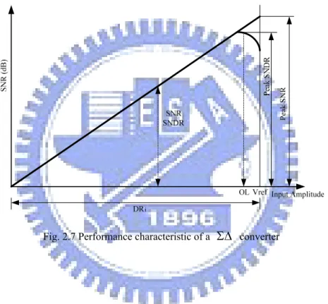
Fig. 2.7 Performance characteristic of a ΣΔ converter………...13
Fig 3.1 Distribution of VS obtained in three cases………18
Fig.3.2 VS versus settling error in three cases……...19
Fig.3.3 The distribution of angle of VS……...19
Fig.3.4. the expect value of (3.16) and the behavior model simulation result……….21
Fig.3.5. The expect value of VS 3 and the simulation result by behavior model……...22
Fig. 3.6. The expect value of VS 5 and the simulation result by behavior model……..22
Fig. 4.1 3D plot of(4.3)………...25
Fig. 4.2 Output spectrum of a second-order ΣΔ modulator with harmonic distortion………...………26
Fig. 4.3 GBW v.s HD3……….27
Fig. 4.4 SR v.s HD3...…28
Fig. 5.1 Circuit-level schematic of spice simulation………29
Fig. 5.2 Quantizer of spice simulation……….29
Fig. 5.3 Comparison of our theoretical result with transistor-level and behavior simulation result………...………30
Fig. 5.4 PSD of settling noise obtained from transistor-level simulation and previous established model……….32
List of Symbols
Symbols
VLSB Quantizer step size
OS
V Maximum output swing of op-amp
OSR OverSampling Ratio
n Order of the Sigma-Delta modulator
B Number of bits in the quantizer
S
f
Sampling FrequencyB
f Signal Bandwidth
ref
V Reference Voltage of the quantizer
0
A Finite Gain of OTA
in
f Frequency of the input signal
i
φ ith phase of a nonoverlap clock
in
A
Amplitude of input signal.
jit
σ standard deviation of clock jitter
S
C
Sampling capacitorI
C
Integrating capacitorL
C
Load capacitor of OTALogic
C
The loading capacitors of CMOS logic gatesgate
C The gate capacitances of all CMOS transmission gates
OX
C The capacitance per unit area of the gate oxide
S
V Input signal plus feedback DAC signal
1
τ Time constant of input branch
VS
σ Standard deviation of VS
2
τ Time constant of integrator output settling
i
η percentage of the bottom plate parasitic
T Absolute temperature R Switch ON resistance
N quantizer levels
gm1 Amplifier transconductance Pr() Probability of some condition
.
cap
σ Mismatch of unit capacitance
k Boltzmann’s constant (1.38×10⁻²³) J/K
α OTA noise factor []
Erf Error Function
OTA
I
Total current of the OTAB
I Bias current of each transistor of the input differential pair of OTA
OTA
k The ratio of the total current of the OTA to this bias current 2
cl
f The GBW of the OTA
reff
V The overdrive voltage of the transistor of the input differential pair of
OTA
Cs
k The ratio between the summation capacitance of in all stages and
the one in the first stage
S
C
0
ε
The permittivity of free spaceS
1.Introduction
1.1 Current Status and Background
Sigma-delta( ) A/D converters have been widely used for implementation of analog-to-digital conversion with high-resolution and low-to-moderate bandwidth ranging from 100Hz to 10MHz like audio [1-3], precision measurement [4], mobile communications [5], worldwide interoperability microwave access (WiMAX) system [6], and broadband wireline application like ADSL [7, 8]. Compared to the traditional converters, modulators have several advantages such as superior linearity and accuracy, simple realization, and low sensitivity to circuit imperfection [9], so modulators have become more suitable for high-resolution and low-power designs.
ΣΔ
ΣΔ
ΣΔ
Switched-capacitor (SC) integrators are basic building components for implementation of circuits. Its incomplete transfer of charge and the slewing effect degrade drastically the performance of
ΣΔ
ΣΔ modulators and remains as the most crucial factor that restricts the performance of ΣΔ modulators. The influence increases as sampling frequency increases, since higher sampling frequency shortens the operating time of the integrator so that the integrator settling error rises. Due to the complexity of settling problem, analytic models for related noises and distortions are virtually non-existent. Recently papers considered transient transfer of charge in SC integrators and proposed several time-domain-based behavioral descriptions [10-12], which can be used in behavior simulations. Behavior simulations are time-consuming, indirect, and difficult to separate settling noises from other noises. On the other hand, analytical efforts are actually seen before. In [18-20], a detailed transient analysis for the charge-transfer error was carried out, but only for linear systems. In [21], the distortion due to operational transconductance amplifier (OTA) dynamics has been
analyzed and modeled. It uses power expansion and nonlinear fitting to obtain analytical model to represent harmonic distortion as a function of the slew-rate (SR), gain-bandwidth (GBW), and nonlinear DC gain, but the settling noise was not discussed. It is coarsely assumed in [13] that the settling noise is white and the associated power spectral density (PSD) is constant in the sampling interval, but this is far from reality.
1.2 Motivation and Aim
Designing of modulators is a very complex process. Recently modulator designing based on numerical optimization [13-15] (behavior simulation) is becoming popular, which requires many computing iterations until best performance is achieved. If the best performance achieved still can not meet the design specification, this approach can provide little clue about the dominating noise or distortion. In contrast, design and optimization based on analytical noise and distortion models can be a more efficient and dependable approach [16, 17], as long as all of the important noise and distortion models are available. Although many noise and distortion models are well derived for
ΣΔ ΣΔ
ΣΔ modulators [], analytical model for switched-capacitor(SC) integrators settling noise is never seen in the literature. For the reasons provided in this and previous paragraphs, the major goal of this paper is to provide the settling noise model.
The settling problems of the SC integrators are mainly caused by non-idealities of OTA such as finite dc gain, finite GBW, and SR limitations. Our research shows that these non-idealities create nonlinear transfer characteristics, which not only cause signal distortions, but also reflect high-frequency noises into base band. By employing nonlinear fitting methods and output spectrum prediction techniques, closed forms of settling error and settling distortion analytical models are obtained, and are represented as functions of ΣΔ modulator system parameters. Both behavior simulations and HSPICE circuits are employed to verify these analytical models, and the results show that our analytical models are sufficiently accurate.
1.3 Organization
This paper is organized as follows. In section II, the motivation of modulators settling effect and properties of the input for SC integrator are discussed. The formulation of analytical settling noise power model is presented in section III with an analytical discussion. In section IV, we develop the model to the settling distortion and discuss the relevance with system parameters. In section V, simulation results including transistor-level and behavior model are used to validate the model do an analytical discussion. in section VI, we provide some conclusions.
2.
Formulation of
ΣΔ
Modulators Settling
Problems
There are two purposes in this section. The first is to clearly define the settling error in switched-capacitor integrators. The second is to explore the properties of VS, which
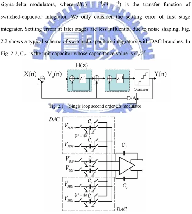
is the input to SC integrator. Fig. 2.1 indicates a standard architecture of second order sigma-delta modulators, where H(z) = z-1
/(1- z-1) is the transfer function of
switched-capacitor integrator. We only consider the settling error of first stage integrator. Settling errors at later stages are less influential due to noise shaping. Fig. 2.2 shows a typical scheme of switched capacitors integrators with DAC branches. In Fig. 2.2, Cμ is the unit capacitor whose capacitance value is Cs/2B.
Fig. 2.1. Single loop second order ΣΔ modulator
2.1 Settling Noise of Sampling Phase and Integration Phase
Sampling and integration phase will be analyzed separately. Fig. 2.3 illustrates sampling and integration phase of SC integrators with the MOS switched on-resistance R and the transconductance of OTA, gm1. Let the output parasitic capacitor be CL ≅η⋅CI , where η is the percentage of bottom plate parasitic,
assumed to be 20%[22]. In Fig. 2.3(a), the voltage VS represents the difference
between the sinusoid input signal and the feedback signal from DAC:
)
(
)
(
)
(
z
X
z
Y
z
V
S=
−
(2.1)In a second-order modulator, modulator output signal Y(z) is the time delay
version of X(z) plus high-pass filtered (noise shaped) quantization noise (1-z-1)2E(z).
Therefore, ΣΔ (2.2)
)
(
)
1
(
)
(
)
(
2 1 2z
E
z
z
X
z
z
Y
=
−+
−
−Combining(2.1)and(2.2), VS (z) can be written as
[
1
]
(
1
)
(
)
)
(
)
(
2 1 2z
E
z
z
z
X
z
V
S=
−
−−
−
− (2.3)It is sampled by Cs, so Cs is charged in the half clock period T/2 to the voltage
VCS: )] 2 exp( 1 [ 1 τ ⋅ − − ⋅ =V T VCS S (2.4)
where is the time constant of the sampling phase in the input branch. So the setting error during the sampling phase is:
s s C R ⋅ = 1 τ
) 2 exp( 1 1 τ ε ⋅ − ⋅ =VS T (2.5) S C S V I C L C VO S V 1 gm I C L C S C R O V S C DAC
(a) Sampling phase (b) Integration phase Fig. 2.3 Switched capacitor integrator diagrams
Next, we consider the integration phase shown in Fig. 2.3(b), where the 2B unit capacitors are combined into Cs, and the 2B DAC switches are neglected. The charge
stored in sampling capacitor will be added to the integration capacitor and this charge current is supplied by OTA. So when the slew rate and gain bandwidth are not large enough, the settling error ε2 will appear. According to absolute value of VS, three
types of settling conditions can happen in the integrator output during this phase, and the corresponding voltage errors of these three conditions are [11]:
1. Linear settling: When the initial change rate of the integrator output voltage (Vo) is
smaller than the OTA slew rate (SR).
) 2 exp( 2 1 2 τ ε ⋅ − ⋅ ⋅ =a VS T , when 2 1 1 0< < ⋅SR⋅τ a VS (2.6)
2. Partial slewing: The initial change rate of Vo is larger than SR, but it gradually
decreases until it is below the slew rate.
1) 2 exp( 2 2 1 2 2 ⋅ − − ⋅ ⋅ ⋅ = τ τ τ ε T SR V a SR S , when 1 2 2 1 ) 2 ( 1 a SR T V SR a ⋅ ⋅τ < S < +τ (2.7)
above SR in the 2 T interval. 2 1 2 T SR V a ⋅ S − ⋅ = ε when ) 2 ( 2 1 τ + > T a SR VS (2.8)
where SR is the slew rate of OTA, and
GBW Cs R GBW ⋅ ⋅ ⋅ ⋅ + = π π τ 2 2 1 2 [23] is the time
constant in the integration phase, with GBW being the equivalent gain bandwidth in the integration phase. The capacitor loading in OTA output during this phase is heavier than in the sampling phase, and is [17]
I S I L S L C C C C C C 2 2 (2 ) + ⋅ + = (2.9) The GBW is given by π 2 2⋅ = L C gm1 GBW (2.10)
2.2 Properties of
VSIn this section, we separately discuss the time-domain and frequency-domain properties of VS to find out the time-domain probability distribution and the P.S.D of.
These properties will be used to do nonlinear fitting and spectrum construction of settling noise in section III.
Firstly, we need to find the VS time-domain statistical property. Simulations results
(using SIMULINK) on a second-order ΣΔ modulator with a1 = 0.5, a2 = 2, 10-level
quantization, reference voltage Vref = 1, and a full scale sinusoidal input signal, are
shown in Fig. 2.4. The result is close to a Gaussian distribution. Therefore, we assume
VS is Gaussian distributed with a zero mean. The standard deviations σVS of VS under
different quantizer levels are tabulated in Table 2.1 We observed that when the quantizer level N increases, σVS decreases. From this table, the relation between standard deviation σVS and quantizer levels 2B can be approximated by
Fig. 2.4. Simulated results of VS distribution
TABLE 2.1
Standard deviations of VS vs. different quantizer bit numbers
Std. deviation (σVS) Variance Quantizer level (N) Bit number (B) 0.706 0.498 2 1 0.476 0.227 3 1.585 0.282 0.080 5 2.322 0.198 0.040 7 2.808 0.152 0.023 9 3.17 0.124 0.016 11 3.46 0.047 0.002 31 4.95
Next, we must determine the P.S.D of VS. Am expression for VS has been given in
(2.3)
[
1]
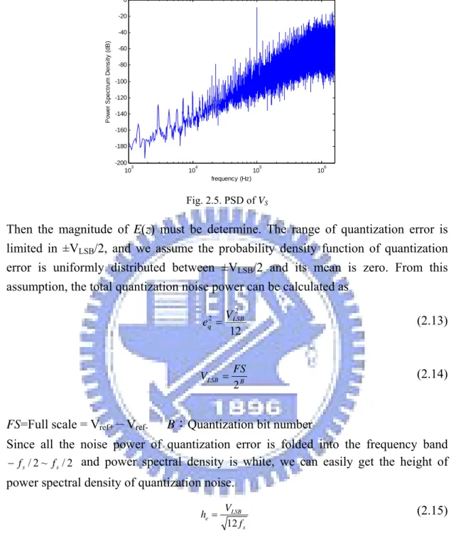
(1 ) ( ) ) ( ) ( 2 1 2 z E z z z X z VS − − − − − =The PSD of VS of second order ΣΔ modulator which simulates with OSR = 16, SR =
60V/μs, GBW = 130M, and a 100kHz sinusoidal input signal is plotted in Fig. 2.5. In
order to calculate the PSD of VS, we separately discuss the part of E(z) and X(z). We
firstly ignore X(z) in (2.3) and express VS as
(2.12) ) ( ) 1 ( ) ( 1 2 z E z z VS − − =
103 104 105 106 -200 -180 -160 -140 -120 -100 -80 -60 -40 -20 0 frequency (Hz) P o w e r S pec tr um D e ns it y (dB ) Fig. 2.5. PSD of VS
Then the magnitude of E(z) must be determine. The range of quantization error is limited in ±VLSB/2, and we assume the probability density function of quantization error is uniformly distributed between ±VLSB/2 and its mean is zero. From this assumption, the total quantization noise power can be calculated as
12 2 2 LSB q V e = (2.13) B LSB FS V 2 = (2.14)
FS=Full scale = Vref+-Vref- B:Quantization bit number
Since all the noise power of quantization error is folded into the frequency band and power spectral density is white, we can easily get the height of power spectral density of quantization noise.
2 / ~ 2 / s s f f − s LSB e f V h 12 = (2.15)
Then we substitute z with ej2πf/fs in (2.12) and magnitude of VS can be defined as
s B s s f FS f f f V 12 2 sin 2 ) ( 2 ⋅ ⎥ ⎥ ⎦ ⎤ ⎢ ⎢ ⎣ ⎡ ⎟⎟ ⎠ ⎞ ⎜⎜ ⎝ ⎛ ⋅ = π (2.16)
So the relationship between the magnitude of VS and the bits number translates to a
Fig. 2.6. Simulated results of VS with AVS = 0.5, OSR = 16, and different Bits
Then we consider the part of X(z) and ignore the E(z) in (2.3) to express VS as
(2.17) ) ( ) 1 ( ) ( 2 z X z z VS − − =
Take the inverse z-transform to (2.17)
) T t ( u ) T t ( x ) t ( x ) t ( VS = − −2 −2 ) 2 ( )) 2 ( sin( ) sin( t A t T u t T Ain − in − ⋅ − = ω ω (2.18)
Then, the amplitude of VS can be obtained as
T A T A T x T V AVS = S(2 )= (2 )= insin(
ω
⋅2 )≅2 in⋅ω
⋅ (2.19)Note that AVS is not related to quantizer bit number B. The result has been verified by
behavior simulation under different B values, as shown in Fig. 2.6. From(2.19), we can see that input signal amplitude Ain, input signal frequency ω and sampling time
T are the critical parameters to impact the harmonic distortion.
2.3 Performance Metrics for a
ΣΔModulator
․Signal to Noise Ratio: The SNR of a data converter is the ratio of the signal power to the noise power, measured at the output of the converter for certain input amplitude. The maximum SNR that a converter can achieve is called the peak
SNR.
․Signal to Noise and Distortion Ratio: The SNDR of a converter is the ratio of the signal power to the power of the noise and the distortion components, measured at the output of the converter for certain input amplitude. The maximum SNDR that a converter can achieve is called the peak SNDR.
․Dynamic Range at the input: The DRi is the ratio between the power of the largest input signal that can be applied without significantly degrading the performance of the converter, and the power of the smallest detectable input signal. The level of significantly degrading the performance is defined as the point where the SNDR is 6 dB bellow the peak SNDR. The smallest detectable input signal is determined by the noise floor of the converter.
․Dynamic Range at the output: The dynamic range can also be considered at the output of the converter. The ratio between maximum and minimum output power is the dynamic range at the output DRo, which is exactly equal to peak SNR.
․Effective Number of Bits: ENOB gives an indication of how many bits would be required in an ideal quantizer to get the same performance as the converter. This numbers also includes the distortion components and can be calculated as
02 . 6 76 . 1 ENOB= SNR− (2.20)
․Overload Level: OL is defined as the relative input amplitude where the SNDR is decreased by 6dB compared to peak SNDR
Typically, these specifications are reported using plots like Fig. 2.7. This figure shows the SNR and SNDR of the ΣΔ converter versus the amplitude of the sinusoidal wave applied to the input of the converter. For small input levels, the
the SNDR and SNR curves coincide for small input levels. When the input level increases, the distortion components start to degrade the modulator performance. Therefore, the SNDR will be smaller than the SNR for large input signals. Note that these specifications are dependent on the frequency of the input signal and the clock frequency of the converter. Fig. 2.7 also shows that SNDR curves drop very fast once the overload point is achieved. This is due to the overloading effect of the quantizer which results in instabilities.
3.
Derivation of Sigma-Delta Modulator
Settling noise Power Model
In this section, models of settling noises which appear at ΣΔ modulator output will be derived and expressed in noise power form. This derivation is divided into sampling phase and integration phase.
3.1 Settling Errors of Sampling Phase
From (15) and (17), we can get magnitude of NTF(z) in frequency domain. By
calculating the sum of in-band noise power, settling error of sampling phase can be acquired.
∫
∫
− − ⎥ ⎦ ⎤ ⎢ ⎣ ⎡ − × = = B B B B f f 2 s s s LSB f f e TF df T f f f V df f N f S P ) 2 exp( ) ( sin 4 12 ) ( ) ( 1 2 2 2 1τ
π
ε (3.1)3.2 Settling Errors of Integration Phase
As discussed in section II, there are three settling conditions depending on the absolute value of VS. The full slewing case is not considered here because it is not
significant. Note that VS at end of each integration interval can be written as
⎪
⎩
⎪
⎨
⎧
>
−
≤
−
=
− L S V V S L S L S S S iV
V
e
e
V
V
V
a
V
V
V
a
V
g
L S)
;
1
(
;
)
1
(
)
(
1 1 1β
β
(3.2)where β =exp(−Ts/2τ2) and VL =SRτ2/ a1
From(3.2),the settling error of integration phase can be calculated as following expression: ⎪⎩ ⎪ ⎨ ⎧ > ≤ = − L S V V L S L S S S V V e e V V a V V V a V L S ; ) sgn( ; ) ( 1 1 1 2
β
β
ε
(3.3)To approximate (3.3), we apply least square method and neglect the even terms by reasons of symmetry of (3.3). Then (3.3) can be approximated by
(3.4) 5 5 3 3 1 ) ( S S S S i V V V V p =α +α +α
The pi(VS) should be fitted through all the points in that specific interval so that the
sum of the squares of the distances of those points from the pi(VS) is minimum. The
sum of the squares is
[
]
S V S S p V dV V q=∫
H − 0 2 2( ) ( ) ε (3.5)[
S V S S S S a V a V a V dV V H 2 0 5 5 1 3 3 1 1 1 2( )∫
− − − =ε
α
α
α
]
With above method, the determination of coefficients in (3.4) for q to be minimum becomes the solution of follow equations.
[
]
[
]
[
]
⎪ ⎪ ⎪ ⎩ ⎪ ⎪ ⎪ ⎨ ⎧ = − ∂ ∂ = − ∂ ∂ = − ∂ ∂∫
∫
∫
0 ] ) ( ) ( [ 0 ] ) ( ) ( [ 0 ] ) ( ) ( [ 0 2 2 5 0 2 2 3 0 2 2 1 S V S S S V S S S V S S dV V p V dV V p V dV V p V H H H ε α ε α ε α (3.6)Note that (3.7) only takes into account the nonlinear curve in (3.7), whereas errors derived from the distribution of VS are omitted. This may lead to a worse estimation of
assumed to be uniformed distributed in the specific integral interval. Nevertheless, the distribution of VS should be defined as Gaussian distribution and the weighting
function that indicates the probability of VS in the specific interval must be considered
so that (3.6) should be de revised as:
[
]
{
}
[
]
{
}
[
]
{
}
⎪ ⎪ ⎪ ⎩ ⎪ ⎪ ⎪ ⎨ ⎧ = × − ∂ ∂ = × − ∂ ∂ = × − ∂ ∂∫
∫
∫
0 ) ( ) ( ) ( 0 ) ( ) ( ) ( 0 ) ( ) ( ) ( 0 2 2 5 0 2 2 3 0 2 2 1 S S V S S S S V S S S S V S S dV V W V p V dV V W V p V dV V W V p V H H H ε α ε α ε α (3.7)where W(VS) represents the weighting function of VS. Since the settling noise is highly
depends on the distribution of VS, the probability of VS in the specific interval must be
defined. As discussed in section II, the VS can be assumed to be Gaussian distribution
and the relation between standard deviation σVS and quantizer levels 2B can be approximated by ref vs B V 1.4⋅ ≈ ⋅σ 2 (3.8) From(3.8), the p.d.f of VS is ) 2 exp( 2 1 ) ( 2 S S V s V s V V f
σ
σ
π
− = (3.9)However, since the integral interval is 0 ~ VH, the p.d.f of VS should be redefined as
) 2 exp( 2 1 ) 2 exp( 2 1 1 ) ( 2 0 2 S S H V s V V s s s V dV V V f
σ
σ
π
σ
π
− − =∫
(3.10)where VH is defined as 2Vref. Then (3.11) is normalized and the weighting function can
) 2 exp( 2 1 ) 2 exp( 2 1 2 0 2 2 S S H V s V V s s H V dV V V k
σ
σ
π
σ
π
− − =∫
(3.11)Taking into account (3.11), (3.8) can be re-written as
[
]
{
}
[
{
]
}
[
]
{
}
⎪ ⎪ ⎪ ⎩ ⎪ ⎪ ⎪ ⎨ ⎧ = × − − − ∂ ∂ = × − − − ∂ ∂ = × − − − ∂ ∂∫
∫
∫
0 ) ( 0 ) ( 0 ) ( 2 0 2 5 5 1 3 3 1 1 1 2 5 2 0 2 5 5 1 3 3 1 1 1 2 3 2 0 2 5 5 1 3 3 1 1 1 2 1 S V S S S S S V S S S S S V S S S S dV k V a V a V a V dV k V a V a V a V dV k V a V a V a V H H H α α α ε α α α α ε α α α α ε α[
]
[
]
[
]
⎪
⎪
⎩
⎪
⎪
⎨
⎧
=
−
×
−
−
−
=
−
×
−
−
−
=
−
×
−
−
−
⇒
∫
∫
∫
0
)
2
(
)
(
0
)
2
(
)
(
0
)
2
(
)
(
2 5 1 0 5 5 1 3 3 1 1 1 2 2 3 1 0 5 5 1 3 3 1 1 1 2 2 1 0 5 5 1 3 3 1 1 1 2 S S V S S S S S S V S S S S S S V S S S SdV
k
V
a
V
a
V
a
V
a
V
dV
k
V
a
V
a
V
a
V
a
V
dV
k
V
a
V
a
V
a
V
a
V
H H Hα
α
α
ε
α
α
α
ε
α
α
α
ε
[
]
[
]
[
]
⎪
⎪
⎩
⎪
⎪
⎨
⎧
=
×
+
+
=
×
+
+
=
×
+
+
⇒
∫
∫
∫
∫
∫
∫
H H H H H H V S S S S V S S S V S S S S V S S S V S S S S V S S SdV
k
V
dV
k
V
V
a
V
a
V
a
dV
k
V
dV
k
V
V
a
V
a
V
a
dV
k
V
dV
k
V
V
a
V
a
V
a
0 2 5 2 2 5 0 5 5 1 3 3 1 1 1 0 2 3 2 2 3 0 5 5 1 3 3 1 1 1 0 2 2 2 0 5 5 1 3 3 1 1 1)
(
)
(
)
(
ε
α
α
α
ε
α
α
α
ε
α
α
α
[
]
[
]
[
]
⎪
⎪
⎪
⎪
⎪
⎪
⎩
⎪
⎪
⎪
⎪
⎪
⎪
⎨
⎧
+
=
×
+
+
+
=
×
+
+
+
=
×
+
+
⇒
∫
∫
∫
∫
∫
∫
∫
∫
∫
− − − H L L S L H H L L S L H H L L S L H V V S S V V L V S S S V S S S V V S S V V L V S S S V S S S V V S S V V L V S S S V S S SdV
k
V
e
e
V
dV
k
V
dV
k
V
V
V
dV
k
V
e
e
V
dV
k
V
dV
k
V
V
V
dV
k
V
e
e
V
dV
k
V
dV
k
V
V
V
2 5 1 0 2 6 2 0 10 5 8 3 6 1 2 3 1 0 2 4 2 0 8 5 6 3 4 1 2 1 0 2 2 2 0 6 5 4 3 2 1β
β
α
α
α
β
β
α
α
α
β
β
α
α
α
Then the values of the coefficients are: × ⎥ ⎥ ⎥ ⎥ ⎥ ⎦ ⎤ ⎢ ⎢ ⎢ ⎢ ⎢ ⎣ ⎡ = ⎥ ⎥ ⎥ ⎦ ⎤ ⎢ ⎢ ⎢ ⎣ ⎡ −
∫
∫
∫
∫
∫
∫
∫
∫
∫
V k V k V k V k V k V k V k V k V k Vh S Vh S Vh S Vh S Vh S Vh S Vh S Vh S Vh S 1 0 10 2 0 8 2 0 6 2 0 8 2 0 6 2 0 4 2 0 6 2 0 4 2 0 2 2 5 3 1 α α α ⎥ ⎥ ⎥ ⎥ ⎥ ⎥ ⎦ ⎤ ⎢ ⎢ ⎢ ⎢ ⎢ ⎢ ⎣ ⎡ + ⋅ + ⋅ +∫
∫
∫
∫
∫
∫
− − − L h L L S L h L L S L h L L S V V V S S V V L S S V V V S S V V L S S V V V S S V V L S S dV V e e V k dV V k dV V e e V k dV V k dV V e e V k dV V k 0 5 1 2 6 2 0 3 1 2 4 2 0 1 2 2 2 β β β β β β (3.12)In order to validate (3.12), we apply least square to the VS in three cases. In case one,
simulations was carried for a ΣΔ modulator with 3-Bits, OSR = 120, SR = 40V /μs,
and GBW = 100MHz and the VS was obtained. The coefficients,α1,α3, and , can be
determined by applying least square method to above VS and compare with the ones
obtained by another two cases, with Gaussian distribution, and no Gaussian distribution. Fig. 3.1 and Table 3.1 show the VS and coefficients obtained in three
cases. The case applied Gaussian distribution show a good fit when compared to the one by simulation. In Fig 3.2, the fitting results in three cases were illustrated and the case with Gaussian distribution is closer to the one simulated than another case. Note that the VL in this case is 0.1681 and the probability of nonlinear operation is respectively 0.35, 0.34, and 0.9 in three cases. This result shows that applying Gaussian distribution to VS plays a crucial role in calculating settling noise.
5 α -0.8 -0.6 -0.4 -0.2 0 0.2 0.4 0.6 0 1000 2000 3000 4000 5000 6000 7000 8000 9000 -0.8 -0.6 -0.4 -0.2 0 0.2 0.4 0.6 0.8 0 2000 4000 6000 8000 10000 12000 -2 -1.5 -1 -0.5 0 0.5 1 1.5 2 0 200 400 600 800 1000 1200 1400
(a) Behavioral model (b) with Gaussian distribution (c) No Gaussian distribution Fig. 3.1. Distribution of VS obtained in three cases
TABLE 3.1
Coefficients obtained in three cases Behavioral model with Gaussian distribution no Gaussian distribution 1 α 0.958 0.94 835.67 3 α 1.239 1.609 -1532.7 5 α 19.677 16.357 567.25 -2 -1.5 -1 -0.5 0 0.5 1 1.5 2 -8000 -6000 -4000 -2000 0 2000 4000 6000 8000 Vs s et tl ing er ro r Behavioral model
with Gaussian distribution no Gaussian distribution
Fig. 3.2. VS versus settling error in three cases
-2 -1.5 -1 -0.5 0 0.5 1 1.5 2 0 200 400 600 800 1000 1200 1400
Fig. 3.3. The distribution of angle of VS
With
α
3 andα
5 , the next step of calculating settling noise power is thedetermination of the P.S.D of VS 3 by using the P.S.D of VS.
The height of the power spectral density of VS in frequency domain can be expressed as α
π
i s s LSB ee
f
f
f
V
f
h
⎥
×
⎦
⎤
⎢
⎣
⎡
=
2)
sin(
2
12
)
(
(3.13)where α represents the angle of VS. In Fig. 3.3, simulation result shows that the
angle of VS is close to a uniform distribution. Therefore, α is considerably assumed
to be a arbitrary value in 0~2π. To demonstrate the P.S.D of VS 3, we will begin by
considering the square of VS. Since the P.S.D VS has been verify in above discussion,
we can use modulation of DTFT Theorems and apply circular convolution to realize square of VS. We can expressed the height of the power spectral density of the square
of VS in frequency domain as
)
(
)
(
)
(
2f
h
f
h
f
h
e=
e⊗
eθ
θ
π
πθ
α d e f f f V f f V f i s s LSB f f s s LSB s s s × ⎥ ⎦ ⎤ ⎢ ⎣ ⎡ − ⎥ ⎦ ⎤ ⎢ ⎣ ⎡ =∫
− 2 2 2 2 ) ) ( sin( 2 12 ) sin( 2 12 1 (3.13)In order to compute the expect value of (3.13), we express (3.13) as a sum of different absolute value with a arbitrary value:
...
+
+
+
β γ α i i ice
Be
Ae
| i A i A i A ... )) sin( ) (cos( )) sin( ) (cos( )) sin( ) (cos( | + + + + + + = γ γ β β α α[
]
0.5 2 2 2 ) cos( ) cos( ) cos( ... ... AB AB AB C B A + − + − + − + + + + = α γ γ β β α (3.14)...
2 2 2+
+
+
C
B
A
(3.15)Then the expect value of the height of spectral density of square of VS can be defined
as
θ
θ
π
πθ
d f f f f V f f h s f f s s LSB s e s s ) ) ( ( sin ) ( sin 9 16 1 ) ( 2 4 2 4 4 2 − =∫
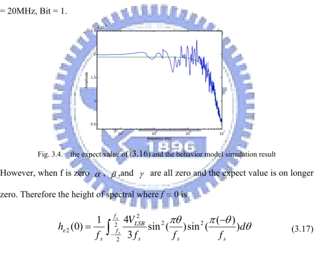
− (3.16)Fig 3.4 shows that the expect value of (3.16) and behavior model simulation with = 20MHz, Bit = 1. S f 104 105 106 107 0.5 1 1.5 2 2.5x 10 -4 A m p lit u d e frequency (Hz)
Fig. 3.4. the expect value of (3.16) and the behavior model simulation result
However, when f is zero α , β,and γ are all zero and the expect value is on longer zero. Therefore the height of spectral where f = 0 is
θ
θ
π
πθ
d
f
f
f
V
f
h
s f f s s LSB s e s s)
)
(
(
sin
)
(
sin
3
4
1
)
0
(
2 2 2 2 2 2−
=
∫
− (3.17)( )
⎪ ⎪ ⎭ ⎪ ⎪ ⎬ ⎫ ⎪ ⎪ ⎩ ⎪ ⎪ ⎨ ⎧ ⎥ ⎥ ⎤ ⎢ ⎢ ⎡ + − + ≅ ) ( cos 8 ) ( cos 136 173 0642 . 0 ) ( sin 879 . 0 2 1 2 4 2 2 2 2 3 3 f f f f f f f f f h s s B e π π π( )
5 . 0 4 4 2 2 2 2 5 5 ) ( sin 8 . 15 ) ( cos 23 . 3 ) ( sin 6 . 55 ) ( cos 11 . 18 ) ( sin ) ( cos 97 . 16 2 . 9 2 0396 . 0 ⎥ ⎥ ⎥ ⎥ ⎥ ⎥ ⎥ ⎦ ⎤ ⎢ ⎢ ⎢ ⎢ ⎢ ⎢ ⎢ ⎣ ⎡ + + + + + ≅ s s s s s s B s e f f f f f f f f f f f f f f h π π π π π πFig. 3.5 and Fig. 3.6shows that the expect value of VS 3 and VS 5 compared with
simulation results by behavior model.
103 104 105 106 107 0 0.5 1 1.5 2 2.5 3 3.5 4 4.5x 10 -4 A m pl it ude frequency (Hz)
Fig. 3.5 The expect value of VS 3 and the simulation result by behavior model
103 104 105 106 107 1 2 3 4 5 6 7 8 9 10x 10 -4 frequency (Hz) A m pl it ud e
Then the expect value of the height of spectral density of settling noise of integration phase can be defined as
5 5 3 3 1 1
)
(
f
h
eh
eh
eh
=
α
+
α
+
α
(3.18)So the settling noise in base band± fBof integration phase can be obtained by
integrating (38): (3.19)
df
f
h
f
h
f
h
P
B B f f e e e∫
−+
+
=
2 5 5 3 3 1 1 2(
α
(
)
α
(
)
α
(
))
εThen total settling noise is
2
1 ε
ε
ε
P
P
P
=
+
(3.20)Note the low frequency region of third and fifth power is absolutely flat and means that the in band noise power will increase if the α3 and α5 in (3.11) increase.
Therefore, the nonlinearity of settling will make an amount increase on noise power. It is worth noting that settling noise is highly dependent on the high frequency noise. Due to the noise shaping nature, the high frequency amplitude of VS is great and will
4.
Derivations of Sigma-Delta Modulators
Settling Distortion
In analysis of settling noise, the input of integrator, VS, is define as a function of
quantization noise and (13) is used to derivate settling noise. However, the VS in this
section is defined as a sinusoid and the quantization noise is ignored.
The technique applied in section 3 will be used to calculate settling distortion. Since the input signal is a sinusoid and the distribution is uniformed distributed in - ~ , the weighting function would not be considered and the coefficients were determined by (25). Then the coefficients were expressed as
VS A AVS ⎥ ⎥ ⎥ ⎥ ⎥ ⎥ ⎥ ⎥ ⎦ ⎤ ⎢ ⎢ ⎢ ⎢ ⎢ ⎢ ⎢ ⎢ ⎣ ⎡ − + ⋅ − − + ⋅ − − + − ⎥ ⎥ ⎥ ⎥ ⎥ ⎥ ⎥ ⎦ ⎤ ⎢ ⎢ ⎢ ⎢ ⎢ ⎢ ⎢ ⎣ ⎡ ⋅ ⋅ − ⋅ ⋅ − ⋅ ⋅ − ⋅ ⋅ − ⋅ = ⎥ ⎥ ⎥ ⎦ ⎤ ⎢ ⎢ ⎢ ⎣ ⎡
∫
∫
∫
∫
∫
∫
VL A VL S S V V S L S S VL A VL S S V V S L S S VL A VL S V V S L S VS L S VS L S VS S L dV V e V V dV V e dV V e V V dV V e dV e V V dV e Vh Vh Vh Vh Vh Vh Vh Vh Vh 0 4 4 0 2 2 0 9 7 5 7 5 3 5 3 5 3 1 ) 1 ( ) 1 ( ) 1 ( ) 1 ( ) 1 ( ) 1 ( 64 11025 32 4725 64 945 32 4725 16 2205 32 525 64 945 32 525 64 225 β β β β β β α α α (4.1) where AVS has defined in (2.19). Note that the validation of the calculation isVS
L A
V < , otherwise, the settling will operate linearly and has no distortion at output
node. VS ≤VL can be further derived as:
L S V V ≤ 5 . 0 2A
ω
T ≤ SRτ
⇒GBW RC GBW SR OSR BW f A S in ⋅ ⋅ ⋅ + ⋅ ≤ × × ⋅ ⋅ ⋅ ⇒ π π π 2 2 1 5 . 0 2 1 2 2 SR RC GBW GBW BW f A OSR S in 5 . 0 2 1 2 2 1 2 2 ⋅ ⋅ + ⋅ × ⋅ ⋅ ⋅ ⋅ ≥ ⇒ π π π (4.2) Assumingfin=BW,R= 300Ω, CS F 12 10 2× −
= , it leads to the following equation:
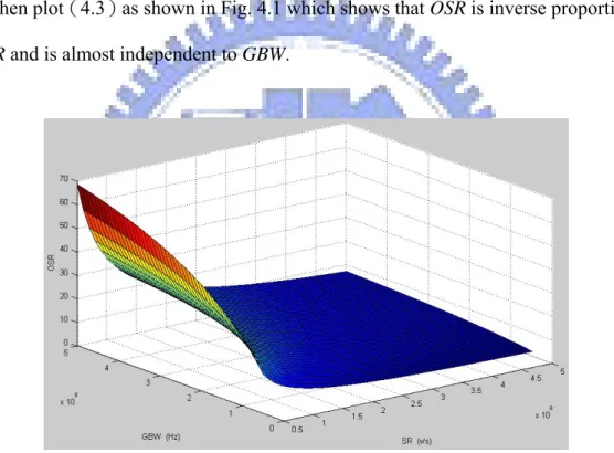
⎟ ⎠ ⎞ ⎜ ⎝ ⎛ + × ⋅ ≥ −10 10 6 2 1 GBW SR OSR π π (4.3) We then plot(4.3)as shown in Fig. 4.1 which shows that OSR is inverse proportional
to SR and is almost independent to GBW.
Fig. 4.1 3D plot of(4.3)
Fig. 4.1 indicates that if we design SR and GBW above the curve with desired OSR, the modulator would have no harmonic distortion. It shows that the op-amp slew rate needs to be at least 200V/us, then the modulator can have no harmonic distortions with OSR larger than 15. Although op-amps operate in linear region can have no harmonic distortion, it may consume more power dissipation (because large slew rate).
Therefore, there has a trade off between power consumption and harmonic distortion. In general, one can choose smaller slew rate to let power consumption lower and have negligible harmonic distortions.
In order to verify the result in (4.1), we use SIMULINK to build a second-order modulator with a multi-bit quantizer. The behavioral settling model in [11] is employed. We assume that SR = 70
ΣΔ
s
V/μ , GBW = 100MHz, R = 300Ω , OSR = 16,
= 1MHz and = 2pF, and a 1MHz sinusoidal input signal is used. After performing FFT to the output data of the modulator, we obtain the simulated P.S.D which is shown in Fig. 4.2 It shows that HD3 is -115.1dB and HD5 is -119.9dB. The theoretical harmonic powers calculated from(4.1) are HD3 = -116.4dB and HD5 = -120.3dB. The simulated and theoretical results are very close, and this confirms that our settling distortion model is reasonably precise.
B f S C ΣΔ 106 107 -250 -200 -150 -100 -50 0 X: 3e+006 Y: -115.1 X: 5e+006 Y: -119.9 frequency (Hz) P o w e r Dens it y (d B )
Fig. 4.2 Output spectrum of a second-order ΣΔ modulator with harmonic distortion
⎟ ⎟ ⎠ ⎞ ⎜ ⎜ ⎝ ⎛ ⎟ ⎟ ⎠ ⎞ ⎜ ⎜ ⎝ ⎛ = 4 2 1 log 20 ) ( 3 3 3 VS settling A dB HD α
20
[
log log(
2)
3 log4 2]
3 + −= α AωT
=20logα3 −60logOSR+30.095 (4.4) 15 . 48 log 100 log 20 ) ( 5 dB = 5 − OSR+ HD settling α
From (4.4) we can see that OSR can effectively influence settling harmonic powers. The(4.4)reveals that α3 and α5 are functions of T, GBW, R, and SR. In order to place much more emphasis on relationship between GBW and the settling distortion, Fig 4.3 shows HD3 with SR=50V/us, R = 300
S C
Ω , OSR = 16, fB= 1MHz and Cs = 2pF,
and a 1MHz sinusoidal input signal. Similarly, Fig. 4.4 shows SR vs. HD3 with
GBW=50MHz. 50 100 150 200 -160 -150 -140 -130 -120 -110 -100 -90 -80 GBW (MHz) HD3 (d B ) Fig. 4.3 GBW v.s HD3
10 15 20 25 30 35 40 45 50 -160 -140 -120 -100 -80 -60 -40 -20 0 SR(V/us) H D 3( dB ) Fig. 4.4 SR v.s HD3
The simulated and theoretical results are very close, and this confirms that our settling distortion model is reasonably precise.
In general, harmonic distortion less than -110dB can be ignored because it is below the noise floor of modulator output spectrum. From(39), Fig. 4.4 and Fig. 4.5, we can obtain the minimum required SR and GBW w. r. t. a specific OSR. The results are summarized in Table 4.4.
It is clear from Table 4.1 that as OSR decreases, SR have to increase dramatically so that the effect of settling distortion can be contained. This can be explained by(39), since T increases when OSR decreases.
TABLE 4.1
Minimum SR and GBW required w. r. t. OSR
OSR HD3(dB) SR ) / (V μs GBW (MHz) 2 20logα3 -24 ≥180 ≥430 4 20logα3 -42 ≥150 ≥400 8 20logα3 -60 ≥120 ≥370 16 20logα3 -72 ≥100 ≥350 32 20logα3 -78 ≥80 ≥340 64 20logα3 -89 ≥50 ≥320 100 20logα3 -90 ≥30 ≥300
Fig. 5.1 Circuit-level schematic of spice simulation
104 105 106 107 -140 -120 -100 -80 -60 -40 -20 frequency (Hz) P ow e r S p ec tr um D e ns it y ( d B ) Behavior Simulation Spice simulation our model (a) 103 104 105 106 107 -120 -100 -80 -60 -40 -20 Behavior Simulation Spice Simulation our model (b) 103 104 105 106 107 -110 -100 -90 -80 -70 -60 -50 -40 -30 -20 -10 frequency (Hz) P o w er S p ec tr um D ens it y ( d B ) Behavior Simulation Spice Simulation Our model (c)
5.
Simulation Results and Validation
In order to demonstrate the validity the model presented in previous section, we use the spice simulation shown in Fig. 5.1 and Fig. 5.2 The relevant parameters were:
kHz, OSR = 100, CS = 0.5pf, Ci = 1pf, and a 100 kHz sinusoidal input signal. Additional parameters used in the simulation of Fig. 5.3 are listed in Table 5.1. Fig. 5.3 shows the settling noise obtained by presented model and simulated output by transistor-level and behavior model. The theoretical noise power by previous model is obtained by adding the previous settling noise power to the theoretical quantization noise power. The output shows a good agreement between the transistor-level modeled and presented modeled modulator.
100 =
B
f
Notice that increase OSR will increase settling noise and reduce SNR. Then we do the same simulation with different OSR. Fig. 5.4 indicates the noise power at modulator output, which is a combination of quantization noise and settling noise. Notice that increasing SR and GBW will reduce settling noise and increase SNR, but will also increase analog power consumption and the design challenges. On the other hand, multi-bit quantizers can reduce the slew rate requirement, since a multi-bit structure makes the output feedback signal closer to the input signal.
20 40 60 80 100 120 140 160 180 -75 -70 -65 -60 -55 -50 -45 -40 In B and N o is e P ow er (dB ) OSR spice simulation presented model
Fig. 5.4 P.S.D of settling noise obtained from transistor-level simulation and previous established model
The previous study reveals that as non-idealities or OSR increases, the settling noise will rise dramatically and degrade the performance of ΣΔ modulator. Because high non-idealities reflect high-frequency noises into base band, first order modulator maybe is a more efficient architecture than second order. In order to make an efficient choice between first and second order, we calculate the minimum required SR and
GBW w. r. t. a specific OSR. The results are summarized in Table 5.2. Table 5.1
indicates that as OSR increase, the bigger SR and GBW are needed to cope with the settling noise.
TABLE 5.1
SIMULATION PARAMETERS IN FIG.5.3
Parameter Fig. 5.3(a) Fig. 5.3(b) Fig. 5.3(c)
SR(V /μ s) 160 80 60
GBW(MHz) 160 127 95
ε
P (dB) -85.4 -68.48 -49.2
TABLE 5.2
MINIMUM SR AND GBW REQUIRED W. R. T.OSR
OSR PQ of fist order
modulator ΣΔ SR ) / (V μ s GBW (MHz) 16 6.69×10⁻⁵ ≥6 ≥20 32 8.37×10⁻⁶ ≥20 ≥40 64 1.05×10⁻⁶ ≥50 ≥75 80 5.35×10⁻⁷ ≥60 ≥120 100 2.74×10⁻⁷ ≥100 ≥140 120 1.59×10⁻⁷ ≥140 ≥160 140 1×10⁻⁷ ≥200 ≥220
6.
Conclusions and Future Works
The analytical model of settling noise of ΣΔ ADCs is never derived in the literature to date and can only be performed through time-domain behavior simulations due to the complex dynamic behavior. In this paper, we have established an analytical model with nonlinear slewing behavior to adequately estimate the ADCs in-band noise power as a function of
ΣΔ ΣΔ modulator system parameters. Once the system parameters such as OSR, GBW, and SR are known, the model gives a expect value of PSD. Both behavior simulations and HSPICE circuits are employed to verify these analytical models, and the results show that our analytical models are sufficiently accurate. Measurement results suggest that for high order ADCs with high OSR and low Bit-number the settling noise will be bigger than other noises and becomes dominate noise source.
References
[1] J. Candy, "A Use of Double Integration in Sigma Delta Modulation," Communications, IEEE Transactions on [legacy, pre - 1988], vol. 33, pp. 249-258, 1985.
[2] B. P. Brandt, D. E. Wingard, and B. A. Wooley, "Second-order sigma-delta modulation for digital-audio signal acquisition," Solid-State Circuits, IEEE Journal of, vol. 26, pp. 618-627, 1991.
[3] B. E. Boser and B. A. Wooley, "The design of sigma-delta modulation analog-to-digital converters," Solid-State Circuits, IEEE Journal of, vol. 23, pp. 1298-1308, 1988. [4] B. DelSignore, D. Kerth, N. Sooch, and E. Swanson, "A monolithic 20 b delta-sigma
A/D converter," in Solid-State Circuits Conference, 1990. Digest of Technical Papers. 37th ISSCC., 1990 IEEE International, 1990, pp. 170-171, 293.
[5] J. Grilo, I. Galton, K. Wang, and R. G. Montemayor, "A 12-mW ADC delta-sigma modulator with 80 dB of dynamic range integrated in a single-chip Bluetooth transceiver," Solid-State Circuits, IEEE Journal of, vol. 37, pp. 271-278, 2002. [6] B. J. Farahani and M. Ismail, "Adaptive Sigma Delta ADC for WiMAX fixed point
wireless applications," Circuits and Systems, 2005. 48th Midwest Symposium on, pp. 692-695, 2005.
[7] R. Gaggl, A. Wiesbauer, G. Fritz, C. Schranz, and P. Pessl, "A 85-dB dynamic range multibit delta-sigma ADC for ADSL-CO applications in 0.18-/spl mu/m CMOS," Solid-State Circuits, IEEE Journal of, vol. 38, pp. 1105-1114, 2003.
[8] R. del Rio, J. M. de la Rosa, B. Perez-Verdu, M. Delgado-Restituto, R.
Dominguez-Castro, F. Medeiro, and A. Rodriguez-Vazquez, "Highly linear 2.5-V CMOS /spl Sigma//spl Delta/ modulator for ADSL+," Circuits and Systems I: Regular Papers, IEEE Transactions on [Circuits and Systems I: Fundamental Theory and Applications, IEEE Transactions on], vol. 51, pp. 47-62, 2004.
[9] S. R. Norsworthy, R. Schreier, and G. C. Temes, Delta-Sigma data converters: theory, design, and simulation: New York: IEEE Press: Wiley-Interscience, 1997.
[10] G. Suarez, M. Jimenez, and F. O. Fernandez, "Behavioral Modeling of Switched Capacitor Integrators with Application to 聶聶 Modulators," in Circuits and Systems, 2006. MWSCAS '06. 49th IEEE International Midwest Symposium on, 2006, pp. 709-713.
[11] P. Malcovati, S. Brigati, F. Francesconi, F. Maloberti, P. Cusinato, and A. Baschirotto, "Behavioral modeling of switched-capacitor sigma-delta modulators," Circuits and Systems I: Fundamental Theory and Applications, IEEE Transactions on [see also
Circuits and Systems I: Regular Papers, IEEE Transactions on], vol. 50, pp. 352-364, 2003.
[12] G. Suarez, M. Jimenez, and F. O. Fernandez, "Behavioral Modeling Methods for Switched-Capacitor Σ∆ Modulators," Circuits and Systems I: Regular Papers, IEEE Transactions on [Circuits and Systems I: Fundamental Theory and Applications, IEEE Transactions on], vol. 54, pp. 1236-1244, 2007.
[13] F. Medeiro, A. Perez-Verdu, and A. Rodriguez-Vazquez, Top-Down Design of High-Performance Sigma-Delta Modulators: Kluwer Academic Publishers, 1999. [14] S. Loeda, H. M. Reekie, and B. Mulgrew, "On the design of high-performance
wide-band continuous-time sigma-delta converters using numerical optimization," Circuits and Systems I: Regular Papers, IEEE Transactions on [Circuits and Systems I: Fundamental Theory and Applications, IEEE Transactions on], vol. 53, pp. 802-810, 2006.
[15] O. Bajdechi and J. H. Huijsing, Systematic Design Of Sigma-delta Analog-to-digital Converters: Springer, 2004.
[16] G. I. Bourdopoulos, Delta-SIGMA Modulators: Modeling, Design and Applications: Imperial College Press, 2003.
[17] Y. Geerts, M. Steyaert, and W. M. C. Sansen, Design of Multi-Bit Delta-SIGMA A/D Converters: Kluwer Academic Publishers, 2002.
[18] W. M. C. Sansen, H. Qiuting, and K. A. I. Halonen, "Transient analysis of charge-transfer in SC filters-gain error and distortion," Solid-State Circuits, IEEE Journal of, vol. 22, pp. 268-276, 1987.
[19] K. L. Lee and R. G. Mayer, "Low-distortion switched-capacitor filter design techniques," Solid-State Circuits, IEEE Journal of, vol. 20, pp. 1103-1113, 1985. [20] J. C. Candy and G. C. Temes, "Oversampling Delta-Sigma Data Converters: Theory,
Design and Simulation," IEEE, New York, 1992.
[21] F. Medeiro, B. Perez-Verdu, A. Rodriguez-Vazquez, and J. L. Huertas, "Modeling opamp-induced harmonic distortion for switched-capacitor ΣΔ modulator design," in Circuits and Systems, 1994. ISCAS '94., 1994 IEEE International
Symposium on, 1994, pp. 445-448 vol.5.
[22] S. Rabii and B. A. Wooley, The design of low-voltage, low-power sigma-delta modulators: Kluwer Academic Publishers Norwell, MA, USA, 1998.
[23] R. Rio Fernandez, F. Medeiro, B. Perez Verdu, J. M. Rosa Utrera, and A. Rodriguez Vazquez, "CMOS Cascade Sigma-Delta Modulators for Sensors and Telecom: Error Analysis and Practical Design," 2008.
Systems, 1999. ISCAS'99. Proceedings of the 1999 IEEE International Symposium on, vol. 2, 1999.