多媒體串流處理器之運算單元設計
69
0
0
全文
(2) An ALU Cluster Design for Media Streaming Processors Architecture. Student. Ting-Wei Lin. Advisor Dr. Herming Chiueh. A Thesis Submitted to Department of Communication Engineering College of Electrical Engineering and Computer Science National Chiao Tung University in Partial Fulfillment of the Requirements for the Degree of Master of Science in Communication Engineering September 2005 Hsinchu, Taiwan..
(3) I.
(4) An ALU Cluster Design for Media Streaming Processors Architecture Student: Ting-Wei Lin. Advisor: Dr. Herming Chiueh. Department of Communication Engineering National Chiao Tung University Hsinchu, Taiwan. Abstract Recent research has proposed using streaming architecture to provide a leap in media applications that are poorly matched to conventional processor architecture. Besides, low power considerations are becoming an important issue for mobile systems, but streaming architecture solutions do not fit in above requirements. Therefore, in this research, a combination of media streaming architecture and low power circuitry design methodology is proposed. An ALU Cluster design for media streaming architecture is presented in this thesis, which is based on Stanford Imagine stream architecture with the consideration of implementation feasibility. The back-end simulation results decide the final micro-architecture of each component, and utilize communication bandwidth hierarchy design to effectively solve the problem of scarce memory bandwidth. The experimental results show that the power and energy consumption of selected benchmark for multimedia and baseband communication systems become scalable by dynamic selecting the number of utilized ALU Clusters. Thus, the instant performance and energy consumption of an entire work can be optimized for mobile systems. The proposed design has provided a breakthrough for similar architectures. II.
(5) ACKNOWLEDGMENTS. This thesis would not have been possible without the support of many exceptional people. First and foremost, thanks go to my research advisor, Professor Herming Chiueh. He has always been an inspiration to me and everyone else on this project through his vision and leadership. He also provided irreplaceable guidance for me when I needed for a fascinating problem, good advice, constructive criticism, support, and flexibility. I would also like to thank all team members of the SoC LAB group, especially my classmates over the years: Elliott Lee, Gary Chan, Maggie Lin, and Uan Cheng. They not only put up with me all of those years, but also made my days as an enjoyable graduate student. Finally, I can not say enough about the support provided by my family. My parents have been my biggest supporters and for that I am forever grateful. My sister and girlfriend have always providing timely encouragement and advice. To all of my friends and family members who have helped me in one way or another over the years, I would like to say thanks.. III.
(6) CONTENTS. ................................................................................................................................I Abstract........................................................................................................................II Acknowledgments......................................................................................................III Chapter 1 Introduction................................................................................................1 Chapter 2 Background.................................................................................................4 2.1 Design Methodology........................................................................................4 2.2 Stream Processing Model.................................................................................9 2.3 Related Research............................................................................................11 2.4 Low Power Considerations............................................................................13 2.5 Media Streaming Processor Architecture.......................................................13 Chapter 3 Design of ALU Cluster Microarchitecture.............................................16 3.1 ALU Cluster Block Diagram..........................................................................16 3.2 Instruction Set Format....................................................................................18 3.3 ALU Cluster Function Units...........................................................................19 3.3.1 ALU Unit.............................................................................................20 3.3.2 MUL Unit............................................................................................21 3.3.3 DIV Unit..............................................................................................22 3.3.4 IRF Unit...............................................................................................23 3.3.5 SPRF Unit............................................................................................24 3.3.6 Decoder Unit.......................................................................................25 3.3.7 Controller Unit....................................................................................25 3.4 System Operation...........................................................................................25 Chapter 4 Implementation.........................................................................................28 4.1 Design Flow....................................................................................................28 4.2 Circuit Implementation and Results...............................................................31 4.3 Circuit Verification and Performance Evaluation….......................................35 IV.
(7) Contents. 4.3.1 Test Bench: FIR Filter.........................................................................35 4.3.2 Functionality Verification....................................................................37 4.3.3 Performance Evaluation Results.........................................................41 4.4 Performance Comparison...............................................................................44 4.5 Low Power Techniques Implementation........................................................45 4.6 Summary.........................................................................................................49 Chapter 5 Conclusion.................................................................................................51 Bibliography................................................................................................................52 Appendix A: Summary of the Defined Microcode in Instruction Set....................55 Appendix B: Assembly Code of Test Bench.............................................................57. V.
(8) LIST OF TABLES. Table 3.3.1.1 The Operations Correspond to the ALU Unit.........................................20 Table 3.3.1.2 Synthesis Results Correspond to Different Architecture........................21 Table 3.3.2.1 The Operation Corresponds to the MUL Unit........................................22 Table 3.3.2.2 Synthesis Results Correspond to Different Pipeline Stages...................22 Table 3.3.3.1 The Operations Correspond to the DIV Unit..........................................23 Table 3.3.3.2 Synthesis Results Correspond to Different Architecture........................23 Table 4.2.1. Circuit Summaries..................................................................................31. Table 4.2.2 The Definition of the I/O Ports...............................................................33 Table 4.4.1 Comparison Results................................................................................44. VI.
(9) LIST OF FIGURES. Figure 1.1. Gap between Processor and Memory.......................................................2. Figure 2.1.1 Figure 2.1.2. An Example of ASIC Design..................................................................5 An Example of Platform-Based Architecture Design.............................6. Figure 2.1.3 An Example of Reconfigurable Architecture Design.............................8 Figure 2.2.1 Direct-Form Realization of an FIR Filter System...................................9 Figure 2.2.2 A Simplified Structure of an FIR Filter System....................................10 Figure 2.5.1 Media Streaming Processor Architecture..............................................14 Figure 3.1.1. ALU Cluster Architecture Block Diagram...........................................17. Figure 3.2.1 Instruction Set Format..........................................................................18 Figure 3.3.1 Function Unit Details............................................................................19 Figure 3.3.4.1 IRF Architecture...................................................................................24 Figure 3.4.1 Pipeline Execution Diagram Details.....................................................26 Figure 3.4.2 Sequence Pipeline Operation Diagram.................................................27 Figure 4.1.1 Cell-Based Design Flow.......................................................................30 Figure 4.2.1 Layout of the ALU Cluster...................................................................32 Figure 4.2.2 Floorplan and Pad Assignment.............................................................32 Figure 4.2.3 Die Microphotograph............................................................................34 Figure 4.2.4 Photograph of Prototype with Package.................................................34 Figure 4.3.1.1 Filter Coefficients, Input Data, and Executed Results of the FIR Filter......................................................................................................36 Figure 4.3.2.1 The Overall Operation Flow.................................................................39 Figure 4.3.2.2 The Operation of WRITE Mode...........................................................39 Figure 4.3.2.3 Insertion of Filter Coefficients..............................................................39 Figure 4.3.2.4 Insertion of Input Data..........................................................................40 Figure 4.3.2.5 The Operation of EXECUTION Mode.................................................40 Figure 4.3.2.6 The Operation of READ Mode.............................................................40 Figure 4.3.3.1 The Code Utilization of Each Arithmetic Unit.....................................42 Figure 4.3.3.2 The Memory Utilization for Capacity Usage........................................43 Figure 4.3.3.3 The Memory Utilization for Data Reference........................................43 VII.
(10) List of Figures. Figure 4.4.1 Figure 4.5.1 Figure 4.5.2 Figure 4.5.3 Figure 4.5.4. The Normalized Comparison Results...................................................45 Multi-Cluster Architecture with Low Power Techniques.....................47 Layout of Multi-Cluster with Low Power Equipments........................47 Power Dissipation on the Multi-Cluster Architecture...........................48 Energy Consumption on the Multi-Cluster Architecture......................48. Figure 4.5.5. Future Mobile Multimedia and Communication System Design Trend.....................................................................................................49. VIII.
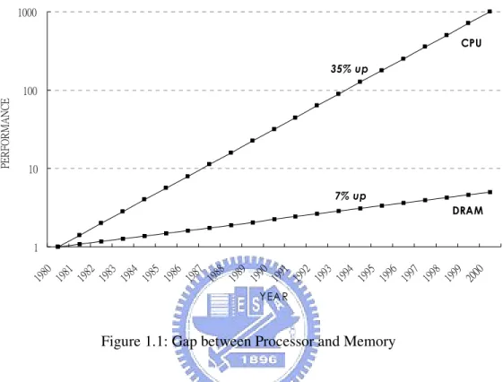
(11) CHAPTER. 1. INTRODUCTION Media processing applications have possession of three key important characteristics: large available parallelism, little data reuse, and a high computation of memory access ratio [1]. However, these characteristics are poorly matched to conventional general-purpose architectures. In the mean time, there is a processor-memory performance gap as well as a memory wall problem arisen that goes off-chip from processor to memory incurs severe latency and bandwidth penalties, as shown in Figure 1.1 [2]. In recent years, the current research has proposed to use the streaming architecture by fitting modern very large scale integrated-circuit (VLSI) technology with lots of arithmetic logic units (ALUs) on a single chip and the hierarchical communication bandwidth design to provide a leap in media processing applications [3][4][5]. Relative topics of recent research are Imagine Stream Processor [6][7][8], Smart Memories [9], and Processing-In-Memory [10][11]. Nevertheless, in contemporary VLSI circuitry for mobile systems, such as handheld audio and video applications, low power considerations are becoming an important issue as battery life and geometry of mobile systems are limited [12]. The streaming architecture and processor-in-memory solutions do not fit in above requirements since it generally occupies a huge die size to trade for the data and processing parallelism. Thus, in recent developments, most of these architectures are focused on the super computing architectures rather than the media processing applications. However, the streaming architecture has been suggested as an efficient architecture for both media processing applications and baseband architecture by using the software defined radio mechanism [13][14]. In order to design the next generation portable multimedia and communication systems, the power dissipation of such a system is an emergency issue. Therefore, a low-power ALU Cluster for the streaming architecture is proposed, which combines the software-defined mechanism -1-.
(12) Chapter 1: Introduction. and the modern low-power circuitry technique in the streaming architecture to provide a breakthrough in the operating time and power dissipation in the limited battery power.. Figure 1.1: Gap between Processor and Memory In this thesis, our major motivation is to improve media processing applications weakly matched to conventional processor architectures. In other words, we aim at the micro-architecture design of the 32-bit ALU Cluster for media streaming processor architectures because ALU Cluster is the nexus computation part of the processors and one main factor of increasing high kernel performance. However, two primary problems have been met are the required high computation throughput and the processor-memory performance gap. So our proposed solution methods to solve these performance bottlenecks are concurrency and locality, respectively. Concurrency is to provide abundant data-level parallelism which means moderate multiple function units in one ALU Cluster. Locality is to decrease the use of the global bandwidth to access the high latency off-chip memory, which means the temporary high speed storage units included inside the ALU Cluster that could form the memory bandwidth hierarchy architectures. With these solution methods, the performance of the media processing applications can be greatly improved.. -2-.
(13) Chapter 1: Introduction. This thesis focuses on an ALU Cluster architecture design of media streaming processors. The remaining of organization of this thesis is as follow. In Chapter 2, the various design methodology styles, the streaming applications processing model, the current relative research topics, and the proposed media streaming processor architecture are introduced. In Chapter 3, the detail micro-architecture of each components of ALU Cluster is designed. Instruction set format, and overall system pipeline operation from instructions read, data reads, operations execute to outcome writes back are also explained. In Chapter 4, the electronic design automation (EDA) flow of implementing this work is presented. The benchmark simulation, performance evaluation, and comparison to recent related architecture design reports are discussed. Besides, a low power ALU Cluster design under group collaboration is also presented. In Chapter 5, the conclusion of this proposed design is addressed.. -3-.
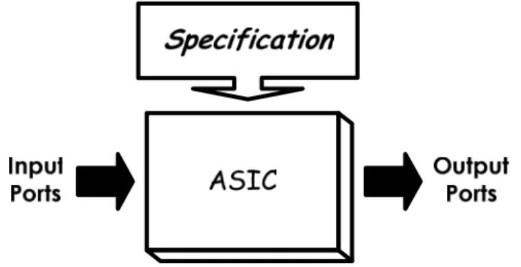
(14) CHAPTER. 2. BACKGROUND In this chapter, a briefly review of the background of the design methodology about three different design implementation styles, and three primary related research topics nowadays about the streaming architectures are described. In addition, the proposed media streaming processor architecture that bases on improving the disadvantages of the current existed streaming architectures is presented.. 2.1 Design Methodology Generally speaking, there are many different methods when implementing a design. In this section, three distinct design methodology styles which are application-specific architecture, platform-based architecture, and reconfigurable architecture will be briefly introduced on the basis of time to market demands, physical area, utilizing flexibility, etc. Furthermore, the pros and cons of these design methodology styles are also discussed. First, the application-specific architecture design is easier among these architectures. Figure 2.1.1 is plotted an example of application-specific integrated circuit (ASIC) design. The chip implementation could be finished quickly as long as following the given well-defined specification. The physical area, operation frequency, and power dissipation could be optimized that depends on demands, too. Nevertheless, the application-specific architecture design is not so flexible and reusable, and needs to redo the overall design flow while the specific applications or specifications are changed.. -4-.
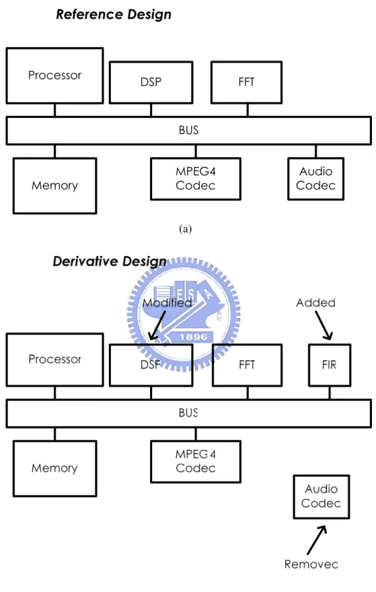
(15) Chapter 2: Background. Figure 2.1.1: An Example of ASIC Design Second, the platform-based architecture design is more flexible than application-specific architecture design. An example of platform-based architecture design is given in Figure 2.1.2. The general platform-based architectures typically include a processor, memory, and communication bus [15]. The intellectual property (IP), such as digital signal processing (DSP), fast Fourier transform (FFT), moving pictures experts group (MPEG) coder and decoder, and audio/video compression and decompression, etc, are all designed with the same protocol of bus and available from the IP libraries to the platform by the application demands. For example, the general platform-based architecture with DSP and audio/video compression and decompression can be used for the video applications, or with DSP and FFT filter can be used for baseband communication. In Figure 2.1.2.(a), the reference design is set for the original specific applications. However, when the specific applications or the required functions are changed, the IP block could be modified, added, and removed to reach the derivatives design which is depicted in Figure 2.1.2.(b). Therefore, the major characteristic of platform-based architecture design is to reduce the design time, since all the devices are based on the same protocol of bus and can be integrated quickly. Unlike application-specific architecture design, the platform-based architecture design could extend to execute more applications by including the extra required IP blocks. In the mean time, the power dissipation will be increased when more and more IP blocks included. The idle unused IP blocks will also waste unnecessary power dissipation. However, in current VLSI circuitry for mobile systems, low power considerations are becoming an important subject since battery life and geometry of mobile systems are limited. Besides, the speed performance will be depended on the slower function units, or mismatch between IP blocks and communication bus. In addition, the scarce memory bandwidth problem between IP blocks and communication bus is not solved totally.. -5-.
(16) Chapter 2: Background. (a). (b) Figure 2.1.2: An Example of Platform-Based Architecture Design. -6-.
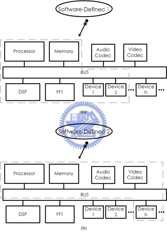
(17) Chapter 2: Background. Third, the reconfigurable architecture is similar to the platform-based architecture design. Some general-purpose IP blocks, such as DSP, FFT, audio/video decoder, and so on, are common blocks for many media processing applications. If a platform-based design includes those general IP blocks, the platform-based design can be used to implement a reconfigurable architecture design. An example of reconfigurable architecture design is depicted in Figure 2.1.3. As shown in Figure 2.1.3.(a), the platform is executed an application for DSP where a additional FFT block is needed to accelerate execution rapidly. If the platform is going to execute another application for MPEG decoder where a audio/video coder and decoder is required, the users only have to reconfigure the data path of IP blocks by implementing the software defined radio mechanism, as shown in Figure 2.1.3.(b). One advantage of the reconfigurable architecture is that the used hardware and data path are reconfigurable. This advantage provides a great flexibility for wide different applications. Nevertheless, on the basis of three chief important media characteristics: large available parallelism, little data reuse, and a high computation of memory access ratio, the reconfigurable architecture could not fit in above requirements well since the bandwidth of communication bus is insufficient and then needs the memory hierarchy architecture to solve this bottleneck. Moreover, the inactive unused IP blocks would increase to dissipate needless energy consumption. This also limits to design for the portable systems at the same time. In conclusion, one of these design methodology styles can be selected to implement that depends on the trade-off of its advantages and disadvantages. As a consequence, the reconfigurable is more suitable to be chosen for the streaming architecture design, because this architecture could provide a significant flexibility in various media processing applications for the software defined radio mechanism.. -7-.
(18) Chapter 2: Background. (a). (b) Figure 2.1.3: An Example of Reconfigurable Architecture Design. -8-.
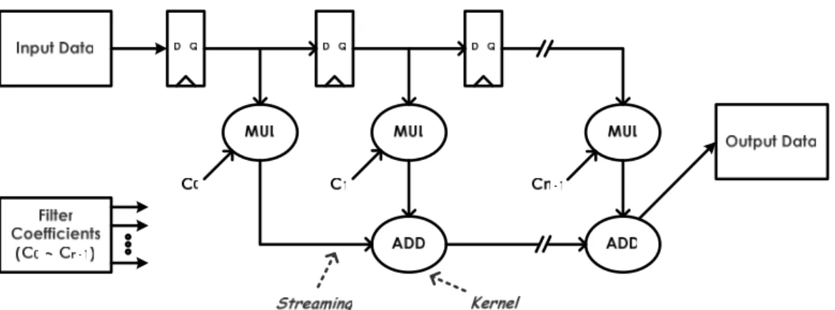
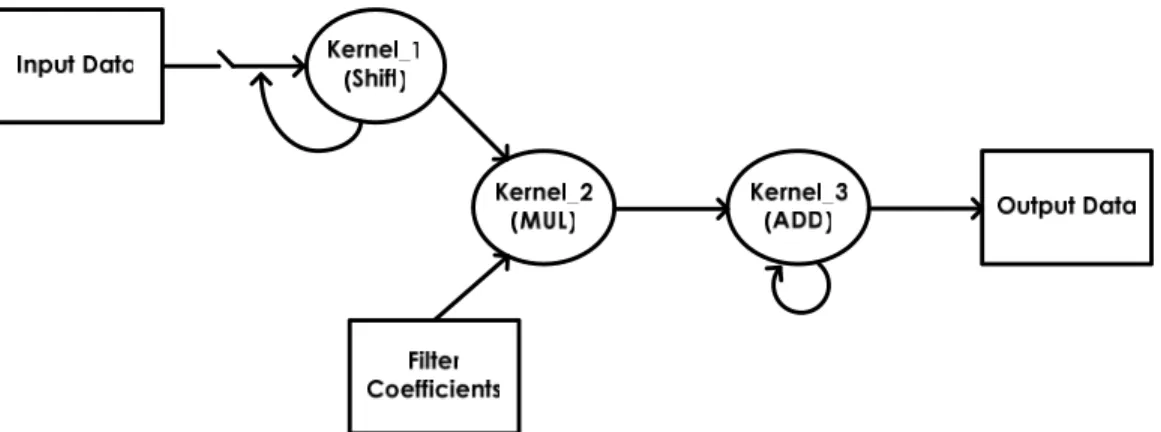
(19) Chapter 2: Background. 2.2 Stream Processing Model Media processing applications are naturally expressed as a sequence of computation kernels that operate on long data streaming [16]. A kernel is a small program that is repeated for each successive streaming element in its input streaming to produce output streaming that is fed to subsequent kernels. Each data streaming is a variable length collection of records, where each record is a logical grouping of media data. In order to illustrate the stream processing model, consider a simple media processing kernel, the finite impulse response (FIR) filter system [17]. An FIR filter is a one dimensional convolution of a small kernel over a long data streaming. Let y[n] represent the output data streaming of an FIR filter. Let T represent the sampled system unit delay which is also equal to the data-rate clock cycle period. At time instant nT the output data sample is given by the following equation describes the operation: y[n ] =. M −1 k =0. bk • x[n − k ]. (2.1). where M represents the number of taps in the filter, bk represents the nth tap coefficient, and x[n] represents the input data sample at time instant nT. The direct-form FIR structure of the difference equation of Equation 2.1 could be realized as shown in Figure 2.2.1. A more simplified structure to be expressed to understand the FIR filter system as well as the stream processing model is also shown in Figure 2.2.2. In both Figure 2.2.1 and Figure 2.2.2, solid arrows stand for data streaming, and ovals stand for computation kernels. Therefore, for example, a record could represent an input data streaming in an FIR filter application. A data streaming, then, could be a collection of hundreds of these input data streaming.. Figure 2.2.1: Direct-Form Realization of an FIR Filter System. -9-.
(20) Chapter 2: Background. Figure 2.2.2: A Simplified Structure of an FIR Filter System Records within a data stream are accessed sequentially and processed identically. This greatly simplifies the movement of data through a media processor by allowing the instruction overhead to be amortized over the length of these homogeneous data streaming. Kernels naturally expose the coarse-grained control parallelism in media processing applications, as they form a pipeline of tasks. Multiple kernels can therefore operate in parallel on different sections of the application’s data. The first kernel in the pipeline would produce output streaming that would then be passed to the next kernel. As the next kernel operates on those streaming, the original kernel could operate on the next set of input data. Finally the memory bandwidth demands of media processing application can also be met using this streaming model. Since all data is organized as streaming, single memory transfer operations initiate long transfers with little control overhead that can be optimized for bandwidth. By organizing media processing applications in this stream processing model, the following characteristics that were enumerated in the previous chapter are exposed: data parallelism is abundant, very little data is reused, and many operations are required per memory reference. Large available parallelism is that operations on one streaming element are largely independent of the others, so they can exploit lots of parallelism and tolerate lots of latency. Little data reuse is that every streaming element is read exactly once from memory and is not revisited, resulting in poor cache performance. A high computation to memory access ratio is that large amounts of arithmetic operations per memory reference are required for each streaming element read from memory. These properties can easily be exploited by a media processor designed to operate on data streaming. The abstraction of a data streaming maps naturally to the streaming data types found in media processing applications. The - 10 -.
(21) Chapter 2: Background. inputs to most media processing applications are already data streaming and the expected outputs are data streaming as well. Streaming exposes the fine-grained data parallelism inherent in media applications as well. Each record of a streaming will be processed identically, so multiple records can be processed in parallel using the same instructions. Therefore, any media processing applications could be organized as the stream processing model, such as shown in Figure 2.2.2, our proposed architecture with reconfigurable characteristic could then utilize the software defined radio mechanism to rearrange the architecture system to suit for implementing various media processing applications flexibly.. 2.3 Related Research On the basis of both the streaming architecture and the processing-in-memory have been recommended as an effective architecture for the media processing applications, relative topics of recent research about the steaming architecture are Imagine Stream Processor, Smart Memories, and Processing-In-Memory. In this section, a brief overview of these three architecture solutions will be introduced. First, Imagine Stream Processor is a programmable single-chip processor that supports the stream programming model. The Imagine architecture supports 48 ALUs organized as 8 single instruction multiple data (SIMD) clusters. Each cluster contains 6 ALUs, several local register files, and executes completely static very long instruction word (VLIW) instructions. The stream register file is the nexus for data transfers on the processor. The memory system, arithmetic clusters, host interface, microcontroller, and network interface all interact by transferring streams to and from the stream register file. Imagine Stream Processor is a coprocessor that is programmed at two levels: the kernel-level and the stream-level. Kernel functions are coded using KernelC, whose syntax is based on the C language. Kernels may access local variables, read input streams, and write output streams, but may not make arbitrary memory references. Kernels are compiled into microcode programs that sequence the units within the arithmetic clusters to carry out the kernel function on successive stream elements. Kernel programs are loaded into the microcontroller' s control store by loading streams - 11 -.
(22) Chapter 2: Background. from the stream register file. At the application level, Imagine Stream Processor is programmed in StreamC. StreamC provides basic functions for manipulating streams and for passing streams between kernel functions. Second, Smart Memories is a multiprocessor system with coarse grain reconfiguration capabilities. Processing units in this system are in form of “Tiles” which when put together in groups of four, form “Quads”. Interconnecting these elements is done in a hierarchical manner: a set of Inter-Quad connections provide communication facilities for Tiles inside a Quad, while a mesh interconnection network connects Quads together. Tiles inside a Quad share the network interface to connect to outside world. Each Tile in the Smart Memories system is consisted of four major parts: Two processor cores, a set of configurable memory mats, a cross bar interconnect, and Load/Store unit. Either or both of the processors inside the Tile can be easily turned off allowing a Tile to be just a memory resource, and saving power, in the case that excess processing power is not required. Third, Processing-In-Memory architectures that integrate processor logic into memory devices offer a new opportunity for bridging the growing gap between processor and memory speeds, especially for applications with high memory-bandwidth requirements. The data-intensive architecture system combines processing-in-memory memories with one or more external host processors and a processing-in-memory-to-processing-in-memory interconnect. Data-intensive architecture increases memory bandwidth through two mechanisms. First, performing selected computation in memory, reducing the quantity of data transferred across the processor-memory interface. Second, providing communication mechanisms called parcels for moving both data and computation throughout memory, further bypassing the processor-memory bus. Data-intensive architecture uniquely supports acceleration of important irregular applications, including sparse-matrix and pointer-based computations. In summary, both the streaming architecture and the processing-in-memory solutions commonly occupy an enormous physical area to trade for the data and processing parallelism without incorporating the well-designed power management equipments. On the other hand, low power considerations have been becoming an essential concern in contemporary VLSI design for portable systems. Therefore, a low power controlling mechanism for the next generation media streaming processor - 12 -.
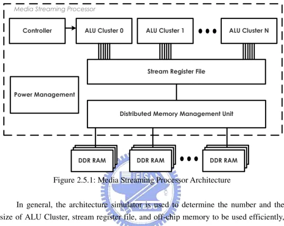
(23) Chapter 2: Background. architecture will be an emergency issue to investigate to provide an advance in the operating time as well as the power dissipation in the future media processing applications.. 2.4 Low Power Considerations Since the power dissipation has turned out to be a significant design concern in modern VLSI design, high power dissipation would incur expensive package and significant cool cost. On the other hand, the power-aware devices, such as laptops, mobile phones, and handhelds devices, etc, have limited advance in battery technology. It is almost a necessity to make the reduction and control of the power dissipation in high performance digital product designs. Techniques for the control and reduction of power dissipation can be divided into two main categories: static and dynamic [18]. Static techniques are typically applied during the circuit design phase and do not change during the operation of the circuit. Dynamic techniques allow the dynamic control of certain functional blocks of the design during functional operation. Dynamic techniques are involved setting certain functional blocks of the chip into low leakage mode when they are in idle mode. Furthermore, if the architecture, such as the platform-based architecture, and the reconfigurable architecture, etc, includes the power management unit, system can scale the power and performance of this architecture. When the required performance is high, more function units on the architecture will be active and consume larger power. While the power consumption of the architecture has to be reduced, system can reduce the active hardware and turn them off with power management unit. So the power and performance of this architecture can be scalable if there is power management unit on the architecture.. 2.5 Media Streaming Processor Architecture By reason of the streaming architecture with software defined radio mechanism has been suggested as an effective architecture for the media processing applications, our proposed improved media streaming processor architecture is depicted in Figure 2.5.1. This architecture primarily includes five components: ALU Cluster, stream - 13 -.
(24) Chapter 2: Background. register file, distributed memory management unit, power management unit, and controller. In the mean time, there is also an architecture simulator that has been built a simulation environment for this architecture.. Figure 2.5.1: Media Streaming Processor Architecture In general, the architecture simulator is used to determine the number and the size of ALU Cluster, stream register file, and off-chip memory to be used efficiently, after simulating a specific media processing application. Therefore, the simulation results from the architecture simulator would then be used with the software defined radio mechanism to reconfigure the media streaming processor. This step would let the system to achieve the best performance that trade between the operating time and the power consumption. The ALU Cluster is used to shorten operating time for the kernel computation. There are also high speed storage units that are embedded in the ALU Cluster to reduce the use of the scarce global communication bandwidth. A controller decodes instructions and then controls the overall operation of all ALU Clusters. The stream register file is a memory organized to handle streaming and could hold any number of streaming of any length. The steam register file supports data streaming transfers between the ALU Cluster and off-chip memory, such as double data rate (DDR) random access memory (RAM), so the recirculation of streaming through the stream register file minimizes the use of scarce off-chip data bandwidth in favor of global register bandwidth. Distributed memory management unit is to solve rare data bandwidth, reduce memory copy, and provide dynamic scheduling. - 14 -.
(25) Chapter 2: Background. Along with the power dissipation has become an important issue concern in modern VLSI circuitry for the mobile systems, a power management unit with low power techniques for the control and reduction of power dissipation has been integrated in the next generation media streaming processor architecture. Furthermore, the power management unit could scale the performance and power by trading for turn on or turn off the function blocks that depend on the simulation results from the architecture simulator. In addition, the high speed storage units inside the ALU Cluster, stream register file, and off-chip memory DDR RAM are formed the memory bandwidth hierarchy architecture. This is in contrast to conventional architectures which use less efficient global register bandwidth when local bandwidth would suffice, in turn forcing the use of more off-chip bandwidth. These main components on the improved media streaming processor and a customized architecture simulator have been under developing at SoC Laboratory by students and faculty. In this thesis, I am chiefly responsible for the design of an ALU Cluster micro-architecture, because ALU Cluster is the nexus computation part of the processors and one key factor of increasing high kernel performance. Besides, the major challenges to complete this work are the architecture decision of each component in the ALU Cluster, met trade-off between timing constraint and area constraint, and complicated to micro-architecture implementation. The detail micro-architecture design and the design flow would be described in the following chapters.. - 15 -.
(26) CHAPTER. 3. DESIGN OF ALU CLUSTER MICROARCHITECTURE In this chapter, the details of an ALU Cluster micro-architecture are discussed from the decision of each component in the ALU Cluster to the integration of these components in the ALU Cluster. In addition, the dedicated instruction set format for the ALU Cluster is also explained. Finally, the pipeline steps and the overall system operation with pipeline mechanism on the ALU Cluster are described.. 3.1 ALU Cluster Block Diagram In order to improve the conventional processor architecture that poorly handle with the media processing applications, two solution methods primarily to solve these performance bottlenecks appeared on the conventional processor architecture, such as the required high computation throughput and the processor-memory performance gap, are concurrency and locality, respectively. Therefore, the proposed 32-bit ALU Cluster micro-architecture design is mainly based on the Stanford Imagine Stream Processor [19][20] with the consideration of the implementation feasibility. Concurrency is to provide abundant data-level parallelism which refers to the computation on different data elements occurring in parallel as well as the moderate multiple function units in one ALU Cluster. Locality is temporal and refers to reuse of coefficients or data during the execution of computation kernels, or is also a form of temporal locality that exists between different stages of a computation pipeline or kernels. So the temporary high speed storage unit is embedded inside the ALU Cluster that could form the memory bandwidth hierarchy architectures to reduce the - 16 -.
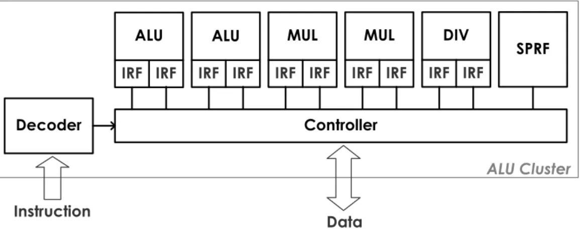
(27) Chapter 3: Design of ALU Cluster Microarchitecture. unnecessary use of global memory bandwidth to access the high latency off-chip memory frequently. The block diagram of the ALU Cluster micro-architecture is shown in Figure 3.1.1.. Figure 3.1.1: ALU Cluster Architecture Block Diagram From Figure 3.1.1, the ALU Cluster architecture are primarily included several arithmetic units, high speed storage units, such as intra-register-file (IRF) and scratch pad register file (SPRF), a decoder, and a controller. The arithmetic units are contained two ALUs, two multipliers, and one divider, supporting to process the large available parallel data simultaneously. Most media processing applications are well suitable for this mixture of arithmetic units. In addition, the back-end simulation results based on the contemporary process technology and the standard cell library could decide the number of parallel arithmetic units. Every arithmetic unit in the ALU cluster is embedded a high speed 32-entry IRF unit for each input. These IRF units mainly are kept to store the temporal intermediate results of computation during executing on streams of data and greatly reduce the usage of the required off-chip memory bandwidth. This allows memory bandwidth to be used efficiently in the sense that expensive and communication limited global memory bandwidth is not wasted on the arithmetic units where inexpensive local memory bandwidth is easy to provide and use. The 64-entry SPRF unit is also an extra high speed storage unit to offer the spills of recirculation of temporary computing data. A decoder fetches instructions and sends the decoded results to the controller. A controller major controls the overall operations of the ALU Cluster. The details of the micro-architecture of these components in the ALU Cluster architecture would be described in the following sections.. - 17 -.
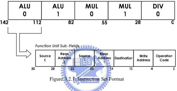
(28) Chapter 3: Design of ALU Cluster Microarchitecture. 3.2 Instruction Set Format The architecture of instruction set format for the ALU Cluster is similar to a VLIW-like instruction format, as shown in Figure 3.2.1. The instruction set format is major composed of fields for the total arithmetic units (ALU units, MUL units, and DIV unit) used in the ALU Cluster. In addition, each arithmetic unit field is further subdivided into sub-field, and each sub-field is contained by the two input sources and their read addresses, the one output destination and its write address, and the executed operation.. Figure 3.2.1: Instruction Set Format The input source reads from three: off-chip data memory, self IRF unit, and SPRF unit. In the same way, the output destination writes back to three: off-chip data memory, one of all IRF units, and SPRF unit. The length of address for input source or output destination is determined by the size of maximum storage unit, for example, one of the off-chip data memory, IRF unit, or SPRF unit. The total executable operation types are depended on different type of arithmetic units, so the length of operation code is also depended on the type of arithmetic units. For example, the length of operation code for the ALU unit, the MUL unit, and the DIV unit is 4-bit, 1-bit, and 2-bit, respectively. Details of operation types of this part will be explained in the next section. The whole length of instruction set would be determined by the total numbers of different type of arithmetic units. The length of the sub-instruction set of each arithmetic unit would be primarily determined by the length of executable operation code. Therefore, for example, the length of the ALU unit, the MUL unit, and the DIV unit is 30-bit, 27-bit, and 28-bit, respectively, and the whole length of instruction set is - 18 -.
(29) Chapter 3: Design of ALU Cluster Microarchitecture. 142-bit. Details summary of the defined microcode in instruction set for the input source, the output destination, and the executable operation of each arithmetic unit are summarized in Appendix A.. 3.3 ALU Cluster Function Units In this section, the micro-architecture design of each function unit in the ALU Cluster would be discussed in the following subsections. A more detailed view of function unit, which is contained an arithmetic unit and its associated register files, is shown in Figure 3.3.1. Most arithmetic units have two data inputs, and output bus. Data in the function unit is temporary stored in the IRF units. These function units are developed with a number of design goals in mind, including the trade-off between physical area, data throughput, and operation latency. As a consequence, in order to reduce the design complexity and enhance the implementation feasibility, Synopsys DesignWare [21] with UMC 0.18 um 1P6M CMOS process and Artisan SAGE-X standard cell library [22] would be used with the intention of shrinking the time of design process.. Figure 3.3.1: Function Unit Details. - 19 -.
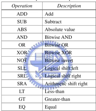
(30) Chapter 3: Design of ALU Cluster Microarchitecture. 3.3.1 ALU Unit An ALU Cluster contains two ALU units that could execute the operations, such as the addition, absolute, logical operation, shift, and comparison instructions, listed in Table 3.3.1.1. Many of these operations support for 32-bit signed integer instructions. These operations could be implemented by using Synopsys DesignWare building block IP, for example, DW01_add, DW01_absval, DW01_ash, and DW01_cmp6. The results of synthesis implementation of available IPs are listed in Table 3.3.1.2. Table 3.3.1.1: The Operations Correspond to the ALU Unit Operation. Description. ADD. Add. SUB. Subtract. ABS. Absolute value. AND. Bitwise AND. OR. Bitwise OR. XOR. Bitwise XOR. NOT. Bitwise invert. SLL. Logical shift left. SRL. Logical shift right. SRA. Arithmetic shift right. LT. Less-than. GT. Greater-than. EQ. Equal. The definition of slack is that the clock period subtracts the library setup time and the data arrival time. Thus, the larger slack value means that more timing margin to complete the execution within one clock cycle. Additionally, the synthesis implementation of available IP only takes the gate delay into consideration without the wire delay, which the wire delay has been grown a chief critical timing issue in the continued scaling of modern VLSI technique [23]. So the larger slack value is better consideration to suitable for the place and route process. The initial clock period is set to 8 ns as well as 125MHz. Besides, the definition of gate count is that the synthesis area of design is divided by the two-input NAND gate area provided by UMC 0.18 um CMOS process with Artisan standard cell library. From Table 3.3.1.2, in order to meet the best optimization between execution time and physical area, therefore, the fast carry-look-ahead architecture is chosen for DW01_add, the carry-look-ahead - 20 -.
(31) Chapter 3: Design of ALU Cluster Microarchitecture. architecture is chosen for DW01_absval, the 2:1 inverting multiplexers and 2:1 multiplexers architecture is chosen for DW01_ash, and the carry-look-ahead architecture is chosen for DW01_cmp6. Finally, the ALU unit is designed as 2-stage pipeline architecture. The first stage is to fetch the data of two inputs from the controller and then decide which operation to be executed from operation code. The second stage is to complete the assigned execution. Table 3.3.1.2: Synthesis Results Correspond to Different Architecture IP. DW01_add. Implementation. Slack. Gate Count. rpl1. 0.56. 244. 2. cla. 2.47. 327. clf3. 5.63. 456. 4. 6.16. 459. 5. 6.09. 705. rpcs6 rpl. 2.33. 342. 2.61. 229. cla. 3.25. 234. bk. csm. DW01_absval. clf. 3.14. 232. 7. 6.30. 916. 8. mx2i. 6.09. 739. mx49. 5.95. 975. 10. mx8 rpl. 5.16. 747. 3.36. 235. bk. 5.71. 224. cla. 6.34. 196. mx2. DW01_ash. DW01_cmp6. 3.3.2 MUL Unit An ALU Cluster contains two MUL units that could execute the multiplication operation, and the executable operation is listed in Table 3.3.2.1. Like the ALU unit,. 1. rpl = ripple-carry 2. cla = carry-look-ahead 3. clf = fast carry-look-ahead 4. bk = Brent-Kung 5. csm = conditional-sum 6. rpcs = ripple-carry-select 7. mx2 = 2:1 multiplexers 8. mx2i = 2:1 inverting multiplexers and 2:1 multiplexers 9. mx4 = 4:1 and 2:1 multiplexers 10. mx8 = 8:1, 4:1, and 2:1 multiplexers. - 21 -.
(32) Chapter 3: Design of ALU Cluster Microarchitecture. the MUL unit also executes operation to support for 32-bit signed integer instructions. The operation could be implemented by using Synopsys DesignWare building block IP, such as DW02_mult and DW_mult_pipe, too. The results of synthesis implementation of available IPs depended on different pipeline stages are listed in Table 3.3.2.2. Table 3.3.2.1: The Operation Corresponds to the MUL Unit Operation. Description. MUL. Multiply. From Table 3.3.2.2, the more pipeline stages would make the more slack value, but the gate count from the part of pipeline registers increases more significantly. Therefore, in order to trade between the execution time and the physical area, the 3-stage pipeline with Booth encoding Wallace tree architecture is chosen for DW_mult_pipe contained DW02_mult. Finally, the MUL unit is designed as 4-stage pipeline. The first three stages are to fetch the data of two inputs and complete the multiplication execution. The forth stage is to truncate the outcome of multiplication to maximum or minimum expressible value if overflow or underflow is occurred, respectively. Table 3.3.2.2: Synthesis Results Correspond to Different Pipeline Stages IP. DW_mult_pipe. Pipeline Stage. Slack. Gate Count. 3. 3.95. 9873. 4. 4.54. 12084. 3.3.3 DIV Unit An ALU Cluster contains one DIV unit that could execute the operations, such as the division and square root instructions, and these executable operations are listed in Table 3.3.3.1. Like both the ALU unit and the MUL unit, these operations also support for 32-bit signed integer instructions. On the other hand, the DIV unit is not the key kernel performance concerned, therefore, the DIV unit would be suggested not to be pipelined and by increasing the latencies of the execution to trade for shrinking area. These operations could be implemented by using DW_div and DW_sqrt of Synopsys DesignWare building block IP. The results of synthesis implementation of available IPs are listed in Table 3.3.3.2.. - 22 -.
(33) Chapter 3: Design of ALU Cluster Microarchitecture. Table 3.3.3.1: The Operations Correspond to the DIV Unit Operation. Description. DIV. Quotient. REM. Remainder. SQR. Square root. From Table 3.3.3.2, in order to minimize the physical area of the DIV unit by means of increasing execution latencies, therefore, the ripple-carry architecture is chosen both for DW_div and DW_sqrt. Finally, the DIV unit is designed as no pipeline architecture but with a latency of 16 clock cycles for the execution of each time. Table 3.3.3.2: Synthesis Results Correspond to Different Architecture IP. DW_div. DW_sqrt. Implementation. Data Arrival Time. Gate Count. rpl. 194.34. 6628. cla. 83.63. 9127. rpl. 68.23. 1585. cla. 44.44. 1914. 3.3.4 IRF Unit While the ALU unit, the MUL unit, and DIV unit are supported all of the arithmetic operations in the ALU Cluster, an important non-arithmetic operation is supported by the IRF unit. The IRF unit is a one read port and one write port high speed register file, and the flip-flops are used as the basic storage element for the IRF units, as shown in Figure 3.3.4.1. The storage capacity of IRF unit is 32 words. The multi-level multiplexer trees are taken the place of the single-level multiplexer trees to speed up the combinational circuit’s part of multiplexer. The IRF unit could be written one data and read another data within the same clock cycle, and the flip-flops before the read selects of IRF unit enable the register file holding the input values within the IRF units so that data written on one clock cycle could be read correctly by the arithmetic unit in the subsequent clock cycle. The key function of IRF unit is major kept to store the temporal intermediate results of calculation during executing on streams of data and significantly decrease the usage of the necessary off-chip memory bandwidth. This allows memory bandwidth to be used efficiently in the sense that the high-cost and communication - 23 -.
(34) Chapter 3: Design of ALU Cluster Microarchitecture. limited global memory bandwidth is not wasted on the function units where the low-priced local memory bandwidth is simple to utilize and offer. In conclusion, all IRF units in the ALU Cluster have a total of 320 words, and provide 8 GB/s of peak memory bandwidth for one ALU Cluster.. # ! " $%. Figure 3.3.4.1: IRF Architecture. 3.3.5 SPRF Unit Another non-arithmetic operation is supported by the SPRF unit. The architecture of SPRF unit is analogous to the architecture of IRF unit except for the size of storage capacity. The SPRF unit is a one read port and one write port high speed register file, and the flip-flops are used as the basic storage element for the SPRF units. The storage capacity of SPRF unit is 64 words, and the SPRF unit could provide 0.8 GB/s of peak memory bandwidth for one ALU Cluster. The SPRF unit could be written one data and read another data within the same clock cycle, and the data written on one clock cycle could be read correctly by the arithmetic unit in the subsequent clock cycle. The primary functions of SPRF unit are to hold some spills from IRF units and store common coefficient parameters.. - 24 -.
(35) Chapter 3: Design of ALU Cluster Microarchitecture. 3.3.6 Decoder Unit The decoder unit provides to fetch the VLIW-like 142-bit instructions from the off-chip instruction memory, and then decodes these instructions for the controller. First, the fetched instruction is divided into several segments depended on the number of arithmetic units. Second, none operation instruction segments are discarded and then the leftover instruction segments are transformed to the requested binary code type for the controller. Finally, the decoded results from the decoder are sequenced to the controller.. 3.3.7 Controller Unit The controller provides temporary storage to hold the decoded instructions, and then sequences and issues these decoded instructions to the function units during execution. The controller is divided into two parts: the read control and the write control. The part of read control receives the decoded instructions from the decoder, and then acknowledges the storage unit, such as off-chip memory, IRF unit, or SPRF unit, to read out the desired data to the assigned function unit. On the other hand, the part of write control would hold the decoded instructions till the function unit that has finished the execution, and then acknowledges the destined storage unit to be written back the result of computation. The precise timing mechanism and the exact computation data flow are two essentially tasks for the controller to manage the overall operation of the ALU Cluster.. 3.4 System Operation In order to increase computation throughput and decrease operation period, the system operation with pipeline mechanism has been recommended as one of solution ways to achieve these goals. Therefore, as is naturally done in most high performance processors, the ALU Cluster also operates in a pipelined manner to reach higher instruction throughput. The pipeline execution diagram in the ALU Cluster is depicted in Figure 3.4.1. The complete process of pipeline operation to execute one instruction includes from FETCH, DECOED, READ REGISTER, and EXECUTE 1 ~ N, to WRITE BACK.. - 25 -.
(36) Chapter 3: Design of ALU Cluster Microarchitecture. Figure 3.4.1: Pipeline Execution Diagram Details During the first pipeline stage in the cycle N (FETCH), the decoder fetches and sequences the VLIW-like instructions from the instruction microcode storage. During the decoding stage (DECODE), the decoder decodes the incoming instructions and then delivers the decoded results to the controller. During the register file read stage (READ REGISTER), the controller would manage the data storage unit to be read out the desired data. The desired data major comes from one of the off-chip data memory, self IRF unit, or SPRF unit, and then sends to the dedicated function unit. During the execution stage (EXECUTE), each function unit begins to execute the computing operation if it has been assigned. The duration of executing clock cycle is depended on the types of function unit, for example, the ALU unit is 2 clock cycles, the MUL unit is 4 clock cycles, and the DIV unit is 16 clock cycles. Finally, during the register file write stage (WRITE BACK), the computing results from the function unit would be written back to the assigned data storage unit managed by the controller. Similarly, the assigned data storage unit also mainly comes from the off-chip data memory, one of all IRF units, or SPRF unit. In summary, while there are perfectly no any hazards happened among the VLIW-like instructions, the sequence pipeline operation mechanism of ALU Cluster is shown in Figure 3.4.2. Although the VLIW-like instructions are scheduled statically and sequenced to the ALU Cluster, any hazards during execution could cause the succession pipeline operation to stall. Thus, if the hazard is encountered, the instructions issued earlier would continue to be executed, but the instructions issued later should be stalled and then be re-executed after the stall condition is no longer valid.. - 26 -.
(37) Chapter 3: Design of ALU Cluster Microarchitecture. &. '$. '$. &. ( ). '$. '$. &. '$. *. ( ). '$. Figure 3.4.2: Sequence Pipeline Operation Diagram. - 27 -. *. ( ). *.
(38) CHAPTER. 4. IMPLEMENTATION In this chapter, the design of an ALU Cluster micro-architecture, described in previous chapter, would be implemented with the cell-based design method. The EDA flow for the implementation of this design is introduced, and the circuit implementation results are listed. The verification results of this work are discussed from the benchmark choice, the chip configuration for simulation, functionality test verification, to the performance evaluation. Finally, the performance comparisons to current related architecture design, implementation of power saving techniques, and a brief summary of this work are also discussed.. 4.1 Design Flow In order to accomplish the implementation of proposed ALU Cluster micro-architecture, from the defined specifications to the die chip achievement, the feasible methods should be provided to complete this work. For most traditional digital circuit design, the computer-aided design (CAD) tools could be supported to deal with these designs. With the help of CAD tools, the time of circuit design process could be shrunk greatly. Besides, the verification and the debug are easily to be detected and handled. A complete digital circuit design flow with the provided standard cell library, for example, the cell-based design flow, is shown in Figure 4.1.1. Three main CAD tools are used to design this work: simulator, synthesizer, and automatic placement and route (APR). In addition, the major steps of design flow include from the architecture design, register transfer level (RTL), gate-level, physical-level, verification, to tape out. The details of these steps are explained in the following: - 28 -.
(39) Chapter 4: Implementation. 1. Architecture design: This is the initial step to design an integrated circuit (IC). The detail specifications and components of an ALU Cluster should be determined definitely and feasibly. 2. RTL: The determined architecture is stylized by using the hardware description language (HDL) code, such as Cadence NC-Verilog [24], to describe the behavior function of each module. The verification of this step is used Novas Debussy [25] to certify the functionality simulation without taking any timing delays into account. Once functionality simulations of RTL do not match to the required specification, the HDL codes should be corrected, or the architecture would be modified until meeting the demands. 3. Gate-level: After the verification of functionality simulation is met with the specification of architecture design, the synthesizable RTL codes are synthesized by utilizing the CAD tool, such as Synopsys Design Compiler [21], to the logic cells. The targeted technology process and the essential synthesis constraints would be selected and set to meet the performance requirements. The functionality simulation with considering the gate delays would be performed for the pre-layout verification. 4. Physical-level: The synthesizable codes with logic cells would be transformed from the gate level model into the transistor level model in this step. The APR, such as Synopsys Astro [21], could be completed the physical implementation. The basic design flow of APR is included the following sub-steps: the global net connection specification, floor planning setup, timing setup, placement and optimization, clock tree synthesis, global nets connection, routing and optimization, and stream out. The gate delay and wire delay would be taken into consideration when performing the post-layout functionality simulation checks. 5. Verification: Another two post-layout verifications are also necessary. One is the design rule check (DRC), and the other is the layout versus schematic (LVS). DRC checks the data of physical layout against the design rules of fabrication, because the design rule document is golden for each design to have to be followed. LVS checks the connectivity of physical layout to its relative schematic circuit netlist. The Mentor Calibre [26] could be used for these verifications. 6. Tape-out: The ultimate physical layout would be produced after having gone through the overall design flow, and then it could be fabricated in the foundry. - 29 -.
(40) Chapter 4: Implementation. Figure 4.1.1: Cell-Based Design Flow. - 30 -.
(41) Chapter 4: Implementation. 4.2 Circuit Implementation and Results The summary of circuit characteristics of this work are listed in Table 4.2.1. UMC 0.18 um CMOS process and Artisan design kit are utilized for the implementation. The post-layout operation frequency of an ALU Cluster is 100MHz. The chip size, core size, gate count, and power dissipation are about 3 mm2, 2.2 mm2, 411491, and 968 mW, respectively. There are total fifteen memories included in this work. The four 32 x 128 single port static RAM (SRAM) and one 14 x 128 single port SRAM are the instruction memory, which is stored the instructions for executing operation. The ten 32 x 32 single port SRAM are the data memory, which is stored the required data for program execution. Without these memories contained in this work, the core size, gate count, and power dissipation are near 1.47 mm2, 255669, and 312 mW, respectively. The physical layout of ALU Cluster is depicted in Figure 4.2.1. The core utilization is close to 88.8%. The floorplan and pad assignment are shown in Figure 4.2.2. There are total 127 input/output (I/O) pads, where 47 input pads, 32 output pads, and 48 power pads. The definition of the I/O ports is summarized in Table 4.2.2. Besides, the die microphotograph of tape-out chip is shown in Figure 4.2.3. The selected package for this chip is CQFP128, and photograph of prototype with package is shown in Figure 4.2.4. Table 4.2.1: Circuit Summaries Technology. UMC 0.18um Mixed Signal (1P6M) CMOS Process. Library. Artisan SAGE-X Standard Cell Library. Clock Rate. 100 MHz. Chip Size. 2.98 x 2.98 mm2. Core Size. 2.2 x 2.2 mm2. (without memory). (1.8 x 1.2 mm2). Gate Count (without memory). 411491 (255669). Power Dissipation. 968.35 mW. (without memory). (312.38 mW). On-Chip Memory. 10 4 1. 32 x 32 32 x 128 14 x 128. single port SRAM single port SRAM single port SRAM. Input: 47 pins Output: 32 pins Power: 48 pins. Pad. - 31 -.
(42) Chapter 4: Implementation. Figure 4.2.1: Layout of the ALU Cluster. #. ". !. ". #$. %. '. &. #$. %. Figure 4.2.2: Floorplan and Pad Assignment - 32 -.
(43) Chapter 4: Implementation. Table 4.2.2: The Definition of the I/O Ports I/O Port Name. I/O. Signal Description. clk. Input. The clock signal provides for this chip.. reset. Input. The reset signal provides for this chip.. This is 4-bit width input. To select one of sel. Input. the instruction memories and the data memories to be written, or one of the data memories to be read.. This input port decides to write or read the data memory. “1” means that data is mem_d_wr. mem_d_ctrl. a. d. Input. written from the off-chip ports to the data memory. “0” means that data is read from the data memory to the off-chip ports.. Input. This input port decides which source signal controls the data memory to be activated. “1” means that the off-chip port controls the enable signal of data memory. “0” means that the on-chip signal controls the enable signal of data memory.. Input. This is 7-bit width input. User can specify the address of instruction memory and data memory by this input port.. Input. This is 32-bit width input. User can insert instructions to the instruction memory and data to the data memory by this input port.. This is 32-bit width output. User can fetch q. Output. execution results from the data memory by this output port.. The power supply provides for the core core_vdd & core_gnd. io_vdd & io_gnd. Power. Power. part of chip. There are total 16 pairs of power supply.. The power supply provides for the I/O part of chip. There are total 8 pairs of power supply.. - 33 -.
(44) Chapter 4: Implementation. Figure 4.2.3: Die Microphotograph. Figure 4.2.4: Photograph of Prototype with Package. - 34 -.
(45) Chapter 4: Implementation. 4.3 Circuit Verification and Performance Evaluation In this section, a selected benchmark is used to show the functionality verification of this work. In order to test with feasibility and ease, three steps of test configuration for this chip would be explained. The functionality simulation and the verification during each step of chip configuration would be also described. Finally, the performance evaluation of this work would be discussed.. 4.3.1 Test Bench: FIR Filter Owing to media processing applications are easily expressed as a series of computation kernels that operate on large data streaming. As long as any media processing application could be organized as the stream processing model that would be suitable for the ALU Cluster to execute, for instance, the FIR filter system has been introduced in previous chapter and is depicted in Figure 2.2.2. The FIR filter system is chosen as the test bench for the ALU Cluster since it is suitable for one dimensional architecture, needs repeat and high percentage of addition and multiplication, and applies for wide DSP applications, such as matched filtering, pulse shaping, equalization, etc. A brief review of FIR filter system is illustrated in the following. The input-output relationship of linear time invariant (LTI) FIR filter can be described as y[n ] =. M −1 k =0. bk • x[n − k ]. (4.1). where M represents the length of FIR filter, bk’s are the filter coefficients, and x[n-k] denotes the data sample at time instance [n-k]. Before executing simulation, the dimension of input and filter coefficients should be determined. As shown in Figure 4.3.1.1(a), the filter coefficients are the sixteen-tap Kaiser window FIR bandpass filters, and the input is an exponential function with ten sampling points. MathWorks Matlab [27] is used to simulate the FIR filter system described above in advance, and the results of simulation are shown in Figure 4.3.1.1(b). This step is in order to make sure the results of FIR filter execution under calculating in the ALU Cluster that could be compared to the results of Matlab simulation to verify whether the functionality operations of this chip work correctly or not.. - 35 -.
(46) Chapter 4: Implementation. 16−th order Kaiser window FIR filter 90. 80. 10−point input function. 10000 9000. 70. 8000. 60 50. 7000. 40. 6000. 30. 5000. 20. 4000. 10. 3000. 0. 2000. −10. 1000. −20 10. 5. 0. 0. 15. 10. 5. 0. (a) FIR output results. 5. 12. x 10. 10 8 6 4 2 0 −2. 0. 5. 15. 10. 20. 25. (b) Figure 4.3.1.1: Filter Coefficients, Input Data, and Executed Results of the FIR Filter. - 36 -.
(47) Chapter 4: Implementation. 4.3.2 Functionality Verification One of design goals for the ALU Cluster is to process the abundant parallel data, so the total numbers of input pads and output pads are enormous significantly. However, the SRAM, such as the instruction memory and the data memory, is utilized to replace and reduce the most of input pads and output pads. Therefore, for the testability and feasibility of this chip, the ALU Cluster would be operated in three different modes: WRITE Mode, EXECUTION Mode, and READ Mode. When this chip is ready to execute programs, it would be operated in the order from WRITE Mode, EXECUTION Mode, to READ Mode. The detail actions of three modes would be described in the following: 1. WRITE Mode: The first step is to insert the instructions and the required data into the instruction memory and the data memory, respectively, from the input port “d.” With combination of the other input ports, such as “sel,” “a,” “mem_d_wr,” and “mem_d_ctrl,” to be controlled and set, user could determine one of the instruction memory or the data memory is the writing target. The value of control signals for memory in this mode are: mem_d_wr = high & mem_d_ctrl = high 2. EXECUTION Mode: After inserting the instructions and the required data into the dedicated memory, the second step is that the ALU Cluster could be begun to execution the assigned programs. In this mode, the input ports, such as “sel” and “a,” are used to control the instruction memory to issue the instructions, and the other input ports, such as “mem_d_wr” and “mem_d_ctrl,” are used to set the data memory to be controlled by the on-chip signals. The value of control signals for memory in this mode are: mem_d_wr = low & mem_d_ctrl = low 3. READ Mode: In the third step, user could read out the data from the data memory for testing after the assigned program execution has been finished. With combination of the input ports, such as “sel,” “a,” “mem_d_wr,” and “mem_d_ctrl,” the computed data could be read out from the data memory to the output port “q.” The logic analyzer could be utilized to confirm that whether the computed results are accurate or not. The value of control signals for memory in this mode are: mem_d_wr = low & mem_d_ctrl = high. - 37 -.
(48) Chapter 4: Implementation. In order to verify functionality of this work, there are three modes to complete a program execution has been described in previous paragraph, and the steps of functionality verification would also follow in this order to be discussed. All functionality verifications are under the environment of post-layout simulation, and the maximal operation frequency is 90.9 MHz for executing the FIR filter system. The overall operation modes are shown in Figure 4.3.2.1. Before executing the assigned programs, the WRITE Mode is executed firstly while having set the input ports, such as “mem_d_wr” is high and “mem_d_ctrl” is high. The ALU Cluster during the WRITE Mode is shown in Figure 4.3.2.2. In this mode, not only instructions are inserted into the instruction memory, but also the filter coefficients and the input data of the FIR filter are inserted into the data memory. Figure 4.3.2.3 and Figure 4.3.2.4 are shown the insertion of filter coefficients and input data, respectively. In addition, the assembly code of overall instructions for the execution of this test bench is summarized in Appendix B. After having completed the WRITE Mode, the EXECUTION Mode could be started. Figure 4.3.2.5 is shown the ALU Cluster operated in the EXECUTION Mode after having set the input ports, such as “mem_d_wr” is low and “mem_d_ctrl” is low. The pre-stored instructions are fetched from the instruction memory to the decoder, and then the controller governs overall ALU Cluster to execute the programs. In the mean time, the required input data is read from the data memory, and only the calculated results are also written back to the data memory. Finally, the last step is to verify the results of program execution. After the WRITE Mode has been finished, this chip is entered into the READ Mode with setting the input ports, such as “mem_d_wr” is low and “mem_d_ctrl” is high. Figure 4.3.2.6 is shown the ALU Cluster worked in the READ Mode. To compare the results read from Figure 4.3.2.6 and the results shown in Figure 4.3.1.1(b), there is no difference between these two results. Therefore, the functionality of ALU Cluster is worked correctly.. - 38 -.
(49) Chapter 4: Implementation. Figure 4.3.2.1: The Overall Operation Flow. Figure 4.3.2.2: The Operation of WRITE Mode Cursor: 0. Marker:0. Delta:0 x 10ps. 80000. 90000. 100000. 110000. 120000. G1. reset. clk. sel[3:0]. 101 -10 -11 -1* -1* -1*. -10 -11 -1* -1* -1* -10 -11 -1* -1* -1* -10 -11 -1* -1* -1* -10 -11 -1* -1* -1* -10 -11 -1* -1* -1* -10 -11 -1* -1* -1*. -10 -11 -1* -1* -1*. -10 -11 -1* -1* -1* -*. mem_d__wr. mem_d__ctrl. a[6:0]. 16. d[31:0]. 11. 1_* 10* 1_*. 0. 1_* 10* 1_*. 0. 1_* -1* 11*. 0. 1_* 10* 11*. 0. 1_* 10* 10*. 0. 1_* 10* 11*. 8. 7. 6. 5. 4. 3. 2. 1. 0. 0. 1_* 10* -1*. 0. 9. 10. 1_* 1_* -1* 11* 10* 1_* -1* -1*. 0. G2. 0. 200000. 400000. 600000. 800000. Figure 4.3.2.3: Insertion of Filter Coefficients ( 1 - 1 ). - 39 -. Page 1.
(50) Chapter 4: Implementation Cursor: 0. Marker:0. Delta:0 x 10ps. 20000. 30000. 40000. 50000. 60000. 700. G1. reset. clk. sel[3:0]. 100. 11. 10. -*. 101. mem_d__wr. mem_d__ctrl. a[6:0]. d[31:0]. 1. 0. 4. 3. 2. 0. 11. 11 -1*. 1. 11. 0 10* 11* 10* 1_* 10* 10* 1_* 10*. 9. 8. 7. 6. 5. 4. 3. 2. 1. 10. 9. 8. 7. 6. 5. 10. 11. 12. 13. 0. -1* 10* -1* 101_01* -1* 10* -1*. 14. 15. 11 -1*. 1. 16. 2. 3. 4. 5. 6. 7. 8. 11 10* 11* 10* 1_* 10* 10* 1_* 10*. 10. 9. 1. 11. 2. 1. 11 -1*. 3. 4. 11. 0. 9. 10. -1* 10* -1* 101_0*. -1*. 5. 6. 7. 8. G2. 0. 200000. 400000. 600000. 800000. Figure 4.3.2.4: Insertion of Input Data Cursor: 0. Marker:0. ( 1 - 1 ). Delta:0 x 10ps. 590000. Page 1. 600000. 610000. 620000. 630000. G1. reset. clk. sel[3:0]. *. 1111. 1010. mem_d__wr. mem_d__ctrl. -35. a[6:0]. 0. 1. 2. 3. 4. 5. 6. 7. 0. 8. 9. 10. 11. 12. 13. 14. 15. 16. 17. 18. 19. 20. 21. 22. 23. 24. 25. 26. 27. 28. 29. 30. 31. 32. 33. 34. 35. 36. 37. 38. 39. 40 *. 0. d[31:0]. G2. 0. 200000. 400000. 600000. 800000. Figure 4.3.2.5: The Operation of EXECUTION Mode Cursor: 0. Marker:0. ( 1 - 1 ). Delta:0 x 10ps. 710000. Page 1. 720000. 730000. 740000. 750000. G1. reset. clk. sel[3:0]. 1111. 101. 0. 20. 1001. mem_d__wr. mem_d__ctrl. a[6:0]. 0. 1. 2. 3. 4. 5. 6. 7. 8. 9. 10. 0. d[31:0]. 0. q[31:0]. 30000. X. -28966. 19347. 7113. -37380. 86248. -158279. 781792. 1127528. 224741. 182620. G2. 0. 200000. 400000. 600000. 800000. Figure 4.3.2.6: The Operation of READ Mode ( 1 - 1 ). - 40 -. Page 1.
(51) Chapter 4: Implementation. 4.3.3 Performance Evaluation Results After having completed the execution of FIR filter system in the ALU Cluster, the results of performance evaluation about the code utilization and the memory utilization could be acquired. The detail performance evaluations are discussed in the following. Figure 4.3.3.1 is shown the code utilization of each arithmetic unit. It takes total 93 instructions for the ALU Cluster to finish the FIR filter simulation. For each arithmetic unit, it takes 60, 75, 80, 80, and 0 instructions for the ALU_0 unit, ALU_1 unit, MUL_0 unit, MUL_1 unit, and DIV_0 unit, respectively, to complete the program execution. Additionally, the code utilization of the ALU_0 unit, ALU_1 unit, MUL_0 unit, MUL_1 unit, and DIV_0 unit is 64.5%, 80.6%, 86%, 86%, and 0%, respectively. Therefore, the code utilization of ALU Cluster is about 63.4%. Besides, it takes 99 clock cycles to complete this simulation, so the clock cycles per executed result output are 3.96. Figure 4.3.3.2 is shown the memory utilization about the capacity usage in the ALU Cluster. The entry size of IRF unit and SPRF unit is 32 and 64, respectively. It needs 10 and 12 reused entries for each IRF unit in the ALU_0 unit and ALU_1 unit, respectively, 16 and 10 reused entries for each IRF unit respectively in both the MUL_0 unit and MUL_1 unit, 3 reused entries for the SPRF unit, and 0 used entries for each IRF unit in the DIV_0 unit during executing the FIR filter simulation. These results have revealed that the initial decisions of storage capacity of IRF unit and SPRF unit are well sufficient to be provided and used during the execution of FIR filter system. Figure 4.3.3.3 is shown the memory utilization about the data reference times in the ALU Cluster. The data reference times mean that the number of times for required data is read or written to the storage units, such as the IRF unit, the SPRF unit, and the off-cluster memory during the program execution. The total number of times for each dedicated off-cluster memory of the ALU_0 unit, ALU_1 unit, MUL_0 unit, MUL_1 unit, and DIV_0 unit to be read/written during executing the FIR filter simulation are 0/21, 0/0, 0/2, 0/0, 16/1, 10/0, 16/1, 10/0, 0/0, and 0/0, respectively. In addition, the total number of times for the SPRF unit and each dedicated IRF unit of the ALU_0 unit, ALU_1 unit, MUL_0 unit, MUL_1 unit, and DIV_0 unit to be read/written during executing the FIR filter simulation are 7/7, 57/57, 56/56, 75/75, 75/75, 80/16, 80/10, 80/16, 08/10, 0/0, and 0/0, respectively. - 41 -.
數據
+7
相關文件
Upon reception of a valid write command (CMD24 or CMD25 in the SD Memory Card protocol), the card will respond with a response token and will wait for a data block to be sent from
² Stable kernel in a goals hierarchy is used as a basis for establishing the architecture; Goals are organized to form several alternatives based on the types of goals and
Reading Task 6: Genre Structure and Language Features. • Now let’s look at how language features (e.g. sentence patterns) are connected to the structure
In the past researches, all kinds of the clustering algorithms are proposed for dealing with high dimensional data in large data sets.. Nevertheless, almost all of
– For each k, the faster, smaller device at level k serves as a cache for the larger, slower device at level k+1. • Why do memory
• Most programs tend to access the storage at any particular level more frequently than the storage at the lower level.. • Locality: tend to access the same set
• When the coherence bandwidth is low, but we need to use high data rate (high signal bandwidth). • Channel is unknown
• When the coherence bandwidth is low, but we need to use high data rate (high signal bandwidth). • Channel is unknown
