Novel Voltage-Mode Universal Filters Using Two Current Conveyors
Ro-Min Weng, Jiunn-Ru Lay, Chih-Lung Lin, and Maw-Huei Lee
Rm.
329, Department of Electrical Engineering, National Taiwan University,No.1 Sec.4, Roosevelt Rd.,Taipei 106, Taiwan, R.O.C. Tel No:886-2-2363525 1 Ext. 329, Fax No: 886-2-23638247
e-mail: d82003@ccsun4.ee.ntu.edu.tw
Abstract
A novel configuration for realizing voltage-mode universal biquad filters with three inputs and two outputs is presented. The configuration uses only two second- generation current conveyors and four passive RC elements. The active and passive sensitivities are quite small. Simulation results that confirm the theoretical analysis are obtained.
1. Introduction
Current-mode circuits have been receiving significant attention because they have the potential adwntages of accuracy and wide bandwidth over their voltage-mode counterparts [l]
.
A number of current- mode amplifiers have been introduced to realize voltage- mode universal filters with three inputs and one output [2]-[6]. Despite the number of active components, those voltage-mode universal filters needed at least five or six passive elements.Among those current-mode amplifiers, second- generation current conveyors (CCIIs) are found useful to realize voltage-mode biquad filters. Over the past few years, several universal filter schemes employing only two CCIIs have been developed [7-[9]. Horng et al. [8]
proposed the filter using only four passive RC elements. We propose a novel configuration for realizing voltage-mode universal biquad filters using only two second-generation current conveyors.The configuration provides three inputs and two outputs employing four passive elements. A number of universal filters can be obtained from the configuration. The proposed filters can realize highpass, bandpass, lowpass, notch, and allpass filters without changing circuit topology and elements. The active and passive sensitivities are quite low. PSpice
simulation are given to verify the theoretical analysis.
2. Circuit bescription
The
wrt
relations of aCCII
can be shownas
0-7803-5146-0/98/$10.00 01998 IEEE.
where the plus and minus signs denote CCII+ and CCII-, respectively. The network symbol and nullor model of CCII k are s h o w in Fig. 1.
The proposed configuration shown in Fig.2 has three inputs and two outputs. By a mutine circuit analysis, the transfer functions of two outputs are given by the following equations:
(2a)
y1y2v11 +2y2y4v~2 +2y3y4v~3
Val = YlY2 +2Y2Y4 +2Y3Y4
-y1y3v11 '('1 +2y4)(y2v~2 "3'13)
v02= Y,Y, +2Y*Y4 +2Y3Y4
According to the nullor model, the first novel voltage- mode universal filter as shown in Fig.3 is presented for YI=sC1, Y2=sC2, Y3=1/R3, and Y4=1/R4. The universal filter, which is called Circuit A, comprises only two CCIIs, CCII+ and CCII-. The transfer functions of two output terminals, V,, and Vo2, can be expressed as
(3a) s2C1C2R3R4Vl, +2sC,R3Vl, +2V1,
(3b) = s2C1C2R,R4 +2sC,R3 + 2
vo,
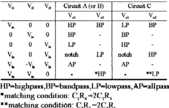
= s2C,C2R3R, +2sC2R3 + 2From Equations (3a) and (3b), five kinds of biquad filters can be realized They are summarized as follows: (i) If V,=V,=O (grounded), a second-order highpass
filter can be obtained from VOl and a second-order bandpass filter can be obtained from V02.
(ii) If V,,=V,=O (grounded),
a
second-order bandpass filter can be obtained from V0l .(iii) If Vll=V,=O (grounded), a second-order lowpass filter
can
be obtained from V,I.
(iv) If
V,=O
(grounded) andVII=Vfi=Vm
,a
second- order notch filter can be obtained fromVo1
and alowpass filter can
be
obtained from Vol.(v) If
VII=-Va=Vu=Vm
, a second-order dbass filter can be obtained from Vol.(vi) If V p O (grounded) and V;I-.V;~-V;~ , a second- order highpass filter can be obtained from Vo2 with matching condition C1Fb=2C2R3.
Th s universal filter is particularly attractive for realizing lowpass filter obtained from Vol because two
-sC1R4V~1 + ( s C l R 4 + 2 ) ( s C 2 R 3 y 2 +y3)
capacitors are grounded. The natural frequency oo and quality factor Q are given by
The natural frequency CO, can be controlled by R3 or R4.
Moreover, the quality factor Q c& be controlled by the ratio of R4R3 or C,/C,.
The second universal filter also shown in Fig.3 is called Circuit B. Its transfer functions, natural frqquency wo, and the quality factor Q are the same as those of Equations (3a), (3b), and (4), respectively.
If we exchange the RC elements of Circuit A, a new universal filter called Circuit C in Fig.3 can be achieved. Its transfer Mctions, natural frequency a,,, and the auality hctor Q are given as
The natural frequency U), can be controlled by R,
or
&.
Moreover, the quality factor Q can be controlled by the ratio of &/Rl or C3/C4. Note that, if V,,=O and V11=V12=Vm , a second-order lowpass filter can be obtained from V,, with matching condition C3& =2C4R,.Five kinds of biquad filters obtained from V,, and V,, , concerning Circuit A, B, and C, are listed in Table 1. From Table 1, one can see that the highpass, bandpass, lowpass, notch and allpass filters can be synthesized from the same output terminal Vol. However, the output terminal V,, can provide only highpass, bandpass, and lowpass filters. The filters require no matching condition except for few applications of V,, Similarly, if the RC elements of Circuit B are exchanged, another universal filter can also
be
obtained The traasfer functions, natural frequency ob and the qwlity Wtbr Q are the same as those of Equations pa}, (5b),and ( 5 93.Sensitivities
Taking
into account the nonideal CCIIs, there are two nonideal factors cc=l f E, (E, denotes the currentt r a G k i n g error from port x to port z) and p=1 -I- ( e2 denotes the voltage tracking error from port y to port x). Note that el and e2 are frequency-dependent compound functions. At low frequency they are real, and exhibit magnitudes that are much lower than unity (q<<l, ~+<<1). The port relations of a nonideal CCII can be given by i,= 31 a i , and vx=flvy. Hence
the natural frequency oo and the quality factor Q of Circuit A become
all of which are small since a v&ue is qpproximately equal to 1. Hence, the proposed universal filters are insensitive to the passive elements they used.
4.Simulation Results
In PSpice simulation, AD844 ICs from Analog
Devices have been used to implement CCIIs. To
evaluate the performance of the Circuit A, consider the typical values for passive elements: C,=C,=lnF,
&
=lkQ, and R4=2kQ. This choice leads to&= 159.2kHz, and Q-1. Fig.4(a) shows the frequency responses of the highpass, bandpass, and lowpass filters obtained from V,, of Circuit A. Circuit B is demonstrated by choosing C, = C, = lnF, R3 = l k n , and R4 = 2kn. Fig.4@) shows the frequency responses of the notch filtei obtained from V,, and lowpass filter obtained from V,, of Circuit B. The gain and phase responses of allpass filter obtained from V,, of Circuit C are shown in Fig 4(c) with C, = C, = lnF, R, = O S W Z , and &=lkSZ. This choice also leads
tofo= 159.2 kHz, and Q = 1.The simulation results are in excellent agreement with the theoretical analysis. 5.Conclusion
A novel configuration for realizing voltage-mode universal filters with three inputs and two outputs is presented. The proposed configuration uses only two
second-generation current cmveyors and four passive dements. A number of voltagc=mo& d v c d filters
can be developed from the c ~ n f i g ~ ~ t t i ~ ~ ~ . The Universal filters can realize the highpass, bandpass, lowpass, notch, and allpass filters without changing circuit toplogy and elements. The proposed configuration provides the following advantages: (i) a number of universal filters
can
be developed fkom thecop&pration, (ii) minimum active and passive elements, (iii) realizing the highpass, bandpass, lowpas, notch, and allpass filters without changing circuit topology and elements, (iv) low active and passive sensitivities. The universal filters require no matching condition except for few applications. All simulation results veritied the theoretical analysis.
References
[ 1 ] Wilson, B., "Recent developments in current conveyors and current mode Circuits", IEE Roc. G,
Circuit Devices Syst., 137, (2), pp.63-77, 1990.
[2] &oguz, S., and Gunes, E.
O.,"
Universal filter with three inputs using CCII+" , Electron. Lett. 32, [3] Chang, C. M. and Lee, M.S., "Comment: Universalvoltage-mode filter with three inputs and one output using three current conveyors and one voltage follower", Electron. Lett., 31, pp.353, 1995. [4] Liu
S.
-I., "Universal filter using two current-feedback amplifiers", Electron. Lett., 31, pp.629-630, 1995.
[5] Abuelma'atti,
M.T.
and Al-Shahrani,S.
M.,
"New universal filter using two current-feedback amplifiers " , I N . J. Electronics, 80, pp.753-756, 1996.[6] Liu, S . 4 , and Lee, J.
-L.,
'lInSensitive current/ voltage-mode filters using FTFNs", Electron. Lett., [71liu,
S. -I., and Lee, J.-La,
"Voltage-mode universalfilter
using INQcurrent conveyors",
INT.
Y, Electronics., 82,pp. 145.149, 1997.[8] Horng, J. -W., Lee, M. -H., Chen, H. -C., and Chang, C. -W.," New CCII-based universal filter using two current conveyors", INT. J. Electronics. [9] Horng, J.
-W.,
Tsai, C. -C., and Lee, M. -H," Noveluniversal voltage biquad filter with three inputs and one output using only two Currefit conveyors",
INT.
J.
Electronics. $0, pp.543-546., 1996. p ~ . 2 134-2 13 5,1996. 32, ~p.1070-1080, 1996. 82, ~p.151-155, 1997. V, V, V, V, 0 0 0 V, 0 0 0v,
V, 0 V,v,
-v, v,
vki vki 0Fig. 1 Symbol and nullor model of CCIIL
C i r a i t A ( o r B ) circuit c VOl vo, v,, vo2 HP BP LP BP BP BP LP HP not& LF' not& HP AP AP 'HP
-
*"LP 0I
Y4Fig.
2connguratlon
for
reamng voltagemode
universal biquad filter
-c
Fig. 3 Proposed voltage-mode universal biquad filters (Circuit A, B, and C)
4(c)
Fig. 4 Simulation results of (a)highpass, lowpass, and bandpass responses from V,, of Circuit A (b) notch filter
from
V,,and
lowpass filter from V,, of Circuit B(c)
gain and phase responses of allpass filter fiom V,, of Circuit C.
Table 1. Five types of biquad filters obtained f'mm V,,
and Vol mnmrning Circiuit 4 B, and C.