Dielectric properties of nitric oxide-annealed gate oxides grown on
nitrogen-implanted silicon substrates
Y.Y. Chen
a,b,⁎
, C.H. Chien
c, J.C. Lou
ca
Computer Science and Information Engineering, Yuanpei Institute of Science and Technology, Hsinchu, Taiwan, ROC
b
Energy and Environment Research Laboratories, Industrial Technology Research Institute, Chutung, Hsinchu, Taiwan, ROC
c
Institute of Electronics, National Chiao-Tung University, Hsinchu, Taiwan, ROC Received 10 November 2004; received in revised form 1 August 2005; accepted 11 January 2006
Available online 28 February 2006
Abstract
The characteristics of nitric oxide (NO)-annealed nitrided gate oxides grown on nitrogen-implanted silicon substrates (NIS) were studied in this paper. It was found that nitrogen accumulation occurred near the interface after NO-annealing, while NIS-grown nitrided oxide produced a uniform nitrogen distribution in the dielectric bulk. Moreover, it was found that the dielectric reliability is strongly dependent on the dosages used
for NIS preparation. NIS with dosages smaller than 1014cm− 2was found not to suppress the oxidation rate and to degrade the dielectric reliability.
On the other hand, the samples with a dosage of 1015 cm− 2not only exhibited a significantly reduced oxidation rate, making it suitable for
growing oxides of multiple thicknesses in sub-3 nm technologies meeting the Systems on Chip requirement, but also improved the dielectric reliability. NO-annealed NIS-grown nitrided oxides depict superior dielectric reliability and this technique appears to be suitable to replace the
traditional SiO2at 0.13μm technology node and beyond.
© 2006 Elsevier B.V. All rights reserved.
Keywords: Nitric oxide (NO); Nitrogen-implanted silicon substrate (NIS); Nitrided oxide; Transmission electron microscopy; Secondary ion mass spectroscopy; Implantation; Gates oxides
1. Introduction
The continuous shrinkage of the dimensions of device features to below a quarter-micron requires highly reliable ultra-thin dielectric films of around 3 nm. In such a ultra-thin oxide regime, the breakdown and wearing out of dielectric films are key technological issues that must be addressed. As an alternative gate dielectric, nitrided oxides have drawn considerable attention due to their superior performance and reliability properties over conventional SiO2 [1–8]. There are two
different primary methods to incorporate nitrogen into gate dielectrics, (I) post-oxidation annealing, including ammonia (NH3), nitrous oxide (N2O) and NO-annealing, and (II) nitrogen
ion implantation into the silicon substrate (NIS) prior to the growth of gate dielectrics. However, NH3annealing introduces
an excessive amount of nitrogen into the gate oxide resulting in reduced carrier mobility along with an excessive amount of hydrogen, which degrades hot carrier immunity[1–3]. Another candidate for nitrogen incorporation, N2O-annealing requires a
much higher thermal budget in order to obtain sufficient nitrogen incorporation[4–6]. As a result, NO-annealing of the initial oxide is preferred in preparing nitrided oxide with sufficient thickness in a reasonable growth time, considering the self-limiting nature of the growth in an NO ambient[6–8].
On the other hand, many efforts, including oxygen, argon and nitrogen implantation are often used to grow multiple gate oxide thicknesses in one thermal cycle in order to meet the Systems on Chip (SoC) requirements[9–14]. Oxygen implan-tation prior to gate oxide growth can improve oxide quality and form multiple oxide thicknesses[9], but it seems unsuitable to the application of deep-submicron generation. Since oxygen implantation will enhance the oxidation rate, the final thickness cannot be scaled down. Reports on argon implantation [10]
indicate that one of the concerns about the argon implantation technique is that the implantation damage caused by heavy mass
⁎ Corresponding author. Computer Science and Information Engineering, Yuanpei Institute of Science and Technology, Hsinchu, Taiwan, ROC. Tel.: +886 3 5917995; fax: +886 3 5835338.
E-mail address: [email protected] (Y.Y. Chen).
0040-6090/$ - see front matter © 2006 Elsevier B.V. All rights reserved. doi:10.1016/j.tsf.2006.01.017
argon ions may need a longer thermal cycle for annealing. In looking at the benefits and drawbacks of the available options, nitrogen implantation can be considered as a proper technology to meet the requirement of deep submicron devices [11–14]. Since nitrogen implantation can retard oxidation rate, it is more suitable to be implemented in SoC technology. Moreover, incorporated nitrogen can be used to suppress boron penetration
[14–16], since it was observed not to be present in both the oxygen and argon implantation techniques. In this paper, the reliability characteristics of the NO-annealed NIS-grown nitrided oxides are studied. Although nitrided oxides degrade flat-band voltage shift and interface state density, the incorpo-ration of nitrogen is demonstrated to effectively suppress trap generation and improve time-to-breakdown (tBD).
2. Experimental details
Local oxidation of silicon (LOCOS) isolated metal-oxide-semiconductor (MOS) capacitors were fabricated on p-type (100) silicon wafers. After forming LOCOS isolation, nitrogen was implanted into the silicon substrates with 10 keV at the splitting dosages of 1013, 1014 and 1015 cm− 2, which are defined as light, medium and heavy NIS dosages, respectively. In addition, some wafers without nitrogen implantation were used for comparison. Wafers were then cleaned and dipped in hydrofluoric (HF) acid before oxidation. The gate dielectrics were grown at 750 °C followed by NO-annealing at 850 °C for 1 h. Then 1500 Å polysilicon was deposited with in-situ doped phosphorus of 1020 cm− 3. Dopants were then activated at 950 °C for 30 s. After gate electrodes patterning and the etching of contact holes, aluminum metallization was done followed by sintering at 450 °C in N2ambient.
Square or circular capacitors of different areas, ranging from 2.5 × 10− 5to 1 × 10− 2cm2, with LOCOS isolation were used to evaluate the integrity of the gate oxide. The physical gate oxide thickness was determined by high-resolution field emission transmission electron microscopy (HR-FETEM), JEOL-2010F. The equivalent oxide thickness (EOT) listed in Table 1 was extracted by fitting the measured high-frequency capacitance– voltage (C–V) data from HP4284 LCR meter under an accumulation condition with quantum mechanical correction
[17,18]. The tunneling leakage current density–gate voltage (J–
V) and the reliability characteristics of MOS capacitors were measured by Semiconductor Parameter Analyzer HP4145A. Nitrogen depth profiles and compositions were analyzed by CAMECA IMS-4f magnetic sector secondary ion mass spectroscopy (SIMS). The microroughness of the wafer surface
and the interface between nitrided oxides/silicon were detected by tapping mode atomic force microscopy (AFM) D3100. 3. Results and discussion
Fig. 1(a) compares the C–V curves of the NO-annealed NIS-grown nitrided oxides. For light and medium NIS dosages, i.e., 1013and 1014 cm− 2, no obvious difference in the C–V curves was observed. However, significant flat-band voltage (VFB)
shift and interface state density (Dit) increment were clearly
evident for the nitrided oxide fabricated with heavy NIS dosages, i.e., 1015 cm− 2. Since nitrogen (N) is a donor-type impurity, the acceptor concentration in the substrate will be compensated by the implanted N atoms before oxidation, resulting in a smaller VFB[11]. It is known that post-oxidation
NO-annealing will introduce N into the gate oxides/substrate interface and, as a consequence, this will lead to the increased VFBshift and Dit[19]. On the contrary, NIS before oxidation
will reduce substrate doping and slightly recover the VFBshift.
The enhanced oxidation rates observed in the nitrided oxides with NIS dosages smaller than 1014 cm− 2 are attributed to insufficient annealing because of the damage created by the ion bombardment, which in turn leads to smaller capacitances. With the heavy implant dosages of 1015cm− 2, the growth rate was found to be reduced by nearly 15%, which seems substantially smaller than the numbers reported in Ref. [13], but this can probably be attributed to the lower oxidation temperature in our
Table 1
EOT, TEM physical thickness and dielectric constant of NO-annealed NIS-grown nitrided oxides
NIS dosage (cm− 2) EOT (nm) TEM (nm) κ
w/o 2.49 2.6 4.0 1013 2.57 2.7 4.1 1014 2.52 2.7 4.1 1015 1.97 2.3 4.6 -2.0 -1.5 -1.0 -0.5 0.0 0.5 0 2 4 6 8 10 12 14 (a) C-V curve Capacitance (fF/ µ m 2) w/o NIS 1013 NIS 1014 NIS 1015 NIS 0.0 -0.5 -1.0 -1.5 -2.0 -2.5 -3.0 10-10 10-9 10-8 10-7 10-6 10-5 10-4 10-3 10-2 10-1 100 101 (b) J-V curve JG (A/cm 2) VG (V) VG (V) w/o NIS 1013 NIS 1014 NIS 1015 NIS
Fig. 1. (a) C–V curves and (b) J–V curves of NO-annealed NIS-grown nitrided oxides.
study. Accompanying the increasing implantation dose, the dielectric constant (κ) was seen to increase from 4.0 of NO-annealed nitrided oxide to 4.6 of NO-NO-annealed NIS-grown nitrided oxide and is summarized inTable 1. J–V curves for the NO-annealed NIS-grown nitrided oxides at negative gate bias are shown in Fig. 1(b). For the cases of 1013 and 1014 cm− 2 dosages, the leakage current increases only slightly because of the residual implantation damages. Nevertheless, for the case of 1015cm− 2dosages, the leakage current density increases more
substantially because the oxidation rate is suppressed by the large amount of the nitrogen incorporation.
Fig. 2 indicates the nitrogen distribution profiles with and without NIS from SIMS analysis. Without NIS the dielectric bulk lacks nitrogen. After post-oxidation NO-annealing, more N will diffuse to interface and form Si3≡N bonds [20].
Moreover, the sample with 1015cm− 2dosages not only exhibits higher peak concentration at the interface, but also has tighter N distribution than the samples with smaller NIS dosages.Fig. 3
(a) compares the transient trapping behavior of NO-annealed NIS-grown nitrided oxides during constant current stress (CCS). It should be noted that all samples show apparent hole trapping characteristics. For dosages less than 1014 cm− 2, pre-oxidation nitrogen implantation will enhance the hole trapping. As the NIS dosages increase to 1015 cm− 2, the hole trapping becomes negligible. The trap generation rate as a function of injected charges is shown in Fig. 3(b). Eliminated trap generation rates are only visualized in samples with heavy N implantation, i.e., 1015 cm− 2. Fig. 4 presents the time-dependent dielectric breakdown (TDDB) Weibull distribution of NO-annealed NIS-grown nitrided oxides during constant voltage stress (CVS) at −4.3 V. Nitrided oxides with NIS dosages smaller than 1014cm− 2reveal much poorer tBDthan the
0 2 4 6 8 10 12 14 16 1018 1019 1020 1021 1022 Nitrogen concentration (cm -3) Depth (nm) w/o NIS 1014 NIS 1015 NIS
Fig. 2. SIMS nitrogen depth profiles of NO-annealed NIS-grown nitrided oxides. 0 20 40 60 80 100 0 10 20 30 40 50 w/o NIS 1014 NIS
(a)transient hole trapping
1013 NIS
1015 NIS
VG
Shift (mV)
Stressing Time (sec)
0 -1 -2 -3 -4 -5 0 2 4 6 8 1015 NIS w/o NIS 1013 NIS 1014 NIS
(b)trap generation rate
Trap Generation Rate (%)
Injected Charges (C/cm2)
Fig. 3. (a) Transient hole trapping behaviors and (b) trap generation rates of NO-annealed NIS-grown nitrided oxides under−20 mA/cm2CCS.
100 101 102 103 104 -3 -2 -1 0 1 2 3 ln(-ln(1-F)) Time (sec) w/o NIS 1013 NIS 1014 NIS 1015 NIS
Fig. 4. tBD Weibull distribution of NO-annealed NIS-grown nitrided oxides
under−4.3 V CVS. 0.05 0.10 0.15 0.20 0.25
AFM Surface Roughness
w/o 1013 1014 1015
RMS Surface Roughness (nm)
NIS Dosage (cm-2)
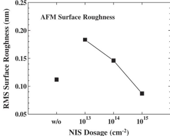
Fig. 5. Silicon surface roughness of NO-annealed NIS-grown nitrided oxides after the removal of the dielectrics.
samples without NIS, due to the larger hole-trapping generation rate. Consistent with the results as shown inFig. 3, the sample with heavy NIS dosages is expected to exhibit the largest tBD.
In this present study, NIS dosages less than 1014 cm− 2 slightly increased the oxidation rate due to the insufficient post-oxidation annealing from damage caused by the ion bombardment, as shown in Fig. 1(a). The residual damage may increase the number of weak bonds during oxidation, and result in a worse stress-induced leakage current (SILC) immunity, enhanced trap generation rate and poor tBD.
Inferior surface roughness is also responsible for the degraded dielectric reliability, as seen inFig. 5. On the other hand, the samples with 1015cm− 2NIS dosages not only can be used to grow multiple oxide thickness, but they also produce a significant improvement in reliability. This trend is quite different from the results in the samples with lighter NIS dosages and can be due to several reasons. First, the surface is abounded with N atoms for heavy NIS implantation dosages, which may easily replace weak Si–O bonds, damaged by ion bombardment in the transition region, by strong Si3≡N bonds during oxidation. Second, implantation
would change the interface morphology. From Fig. 5, it is evident that, despite NO-annealing being known for smooth surface morphology [19], roughness is increased when the NIS dosages increase from 0 to 1014 cm− 2, which may be
due to the slightly faster oxidation rates from the damaged surface and less N area density. On the other hand, the surface becomes almost atomically flat when the NIS dosages are further increased to 1015 cm− 2. A smoother interface is helpful in reducing the localized field and hence results in stronger SILC immunity and larger tBD. Cross-sectional TEM
images are shown in Fig. 6. For heavy NIS dosages, the nitrided oxide/silicon interface is very smooth and there is a highly uniform transition region from the crystalline silicon to the amorphous nitrided oxide. This feature is beneficial to the electrical properties of the MOS device as described above. Third, it is known that SILC becomes negligible as the oxide thickness is scaled down to the direct-tunneling dominated regime. The heaviest NIS dosages can significantly retard the oxidation rate and grow the thinnest oxide, as shown inFig. 1
(a). As a consequence, the nitrided oxides with NIS dosages of 1015 cm− 2 cannot only grow multiple oxide thickness to meet SoC requirements, but also possess a stronger SILC immunity and better TDDB characteristics than others. 4. Conclusions
According to the International Technology Roadmap for Semiconductors, oxide thicknesses below 3 nm are necessary for the fabrication of deep sub-quarter micron devices. In the present study, an obvious oxidation rate retardation effect is observed only for the sample with heavy NIS dosages. The dielectric property is also strongly dependent upon the NIS dosages. NIS with dosages smaller than 1014cm− 2is ineffective for oxidation rate suppression and degrades the dielectric reliability characteristic as well. On the other hand, the samples with 1015 cm− 2 NIS dosages not only can be used to grow multiple oxide thickness to meet SoC requirements, but they also improve stress immunity. Nitrogen implantation also generates a uniformly distributed nitrogen profile in the dielectric bulk, which can be used as an effective diffusion barrier to resist against boron penetration. In conclusion, NO-annealed NIS-grown nitrided oxides can improve dielectric reliability, which are suitable for replacing traditional SiO2at
0.13μm and beyond.
References
[1] Z.H. Liu, H.-J. Wann, P.K. Ko, C. Hu, Y.C. Cheng, IEEE Electron Device Lett. 13 (1992) 402.
[2] P. Pan, J. Appl. Phys. 61 (1987) 284.
[3] T. Hori, H. Iwasaki, K. Tsuji, IEEE Trans. Electron Devices 36 (1989) 340. [4] G.W. Yoon, A.B. Joshi, J. Kim, D.L. Kwong, IEEE Electron Device Lett.
14 (1993) 179.
[5] T. Hori, Microelectron. Eng. 22 (1993) 245.
[6] E.P. Gusev, H.-C. Lu, E.L. Garfunkel, T. Gustafsson, M.L. Green, IBM J. Res. Develop. 43 (1999) 265.
[7] M. Fujiwara, M. Takayanagi, T. Shimizu, Y. Toyoshima, Tech. Dig., Int. Electron Devices Meet., San Francisco, U.S.A., Dec. 10–13, 2000, p. 227. [8] T. Ohguro, Y. Okayama, K. Matsuzawa, K. Matsunaga, N. Aoki, K. Kojima, S. Momose, K. Ishimaru, Symp. VLSI Tech. Dig., Kyoto, Japan, June 10–12, 2003, p. 37.
[9] Y.-C. King, C. Kuo, T.-J. King, C. Hu, Tech. Dig., Int. Electron Devices Meet., San Francisco, U.S.A., Dec. 6–9, 1998, p. 585.
Fig. 6. HR-FETEM cross-sectional images of NO-annealed NIS-grown nitrided oxides.
[10] M. Togo, K. Noda, T. Tanigawa, Tech. Dig., Int. Electron Devices Meet., San Francisco, U.S.A., Dec. 6–9, 1998, p. 347.
[11] A. Furukawa, Y. Abe, S. Shimizu, T. Kuroi, Y. Tokuda, M. Inuishi, Symp. VLSI Tech. Dig., Honolulu, U.S.A., June 11–13, 1996, p. 62.
[12] C.T. Liu, Y. Ma, M. Oh, P.W. Diodato, K.R. Stiles, J.R. McMacken, F. Li, C.P. Chang, K.P. Cheung, J.I. Colonel, W.Y.C. Lai, R. Liu, E.J. Lloyd, J.F. Miner, C.S. Pai, H. Vaidya, J. Frackoviak, A. Timko, F. Klemens, H. Maynard, J.T. Clemens, Tech. Dig., Int. Electron Devices Meet., San Francisco, U.S.A., Dec. 6–9, 1998, p. 589.
[13] L.K. Han, S. Crowder, M. Hargrove, E. Wu, S.H. Lo, F. Guarin, E. Crabbé, L. Su, Tech. Dig., Int. Electron Devices Meet., Washington, U.S.A., Dec. 7–10, 1997, p. 643.
[14] J.O. Bark, S.W. Kim, IEEE Electron Lett. 34 (1998) 1887.
[15] B. Yu, D.-H. Ju, W.-C. Lee, N. Kepler, T.-J. King, C. Hu, IEEE Trans. Electron Devices 45 (1998) 1253.
[16] Q. Xu, H. Qian, Z. Han, G. Lin, M. Liu, B. Chen, C. Zhu, D. Wu, IEEE Trans. Electron Devices 51 (2004) 113.
[17] K.J. Yang, C. Hu, IEEE Trans. Electron Devices 46 (1999) 1500. [18] K. Yang, Y.-C. King, C. Hu, Symp. VLSI Tech. Dig., Kyoto, Japan, June
14–16, 1999, p. 77.
[19] B. Maiti, P.J. Tobin, V. Misra, R.I. Hegde, K.G. Reid, C. Gelatos, Tech. Dig., Int. Electron Devices Meet., Washington, U.S.A., Dec. 7–10, 1997, p. 651.
[20] T. Ogata, M. Inoue, T. Nakamura, N. Tsuji, K. Kobayashi, K. Kawase, H. Kurokawa, T. Kaneoka, Y. Ohno, H. Miyoshi, Tech. Dig., Int. Electron Devices Meet., San Francisco, U.S.A., Dec. 6–9, 1998, p. 597.