國
立 交 通 大 學
材料科學與工程學系
碩
碩
碩
碩 士
士
士 論
士
論
論
論 文
文
文
文
CF
4
電漿處理對可撓式聚對苯二甲酸乙二酯基材
水氣穿透率之影響
Effects of CF
4plasma treatment on the WVTR of PET films as
flexible substrate
研 究 生:賴伯政
指導教授:呂志鵬 博士
中華民國
中華民國
中華民國
中華民國
九十九
九十九
九十九
九十九
年
年
年
年
八
八
八
八
月
月
月
月
CF
4電漿處理對可撓式聚對苯二甲酸乙二酯基板水氣穿透率之影響
Effects of CF
4plasma treatment on the WVTR of PET films as flexible substrate
研 究 生:賴伯政 Student:Po Cheng Lai
指導教授:呂志鵬 Advisor:Dr. Jihperng (Jim) Leu
國 立 交 通 大 學
材 料 科 學 與 工 程 學 系
碩 士 論 文
A Thesis
Submitted to Department of Materials Science and Engineering College of Engineering
National Chiao Tung University in partial Fulfillment of the Requirements
for the Degree of Master in
Materials Science and Engineering
CF4 電漿處理對可撓式聚對苯二甲酸乙二酯可撓式基板水氣穿透率之影響 研究生: 賴伯政 指導教授: 呂志鵬 博士 國立交通大學材料科學與工程學系碩士班
摘要
摘要
摘要
摘要
隨著科技的進步,輕、薄、短小、低成本成為主要的訴求,在這樣需要下,可撓式 元件逐漸被重視,雖然高分子基材已經成功應用在可撓式元件上,但當有機物加入可撓 式元件時,高分子基板的高水氣穿透率(WVTR)是一個缺點。水氣會和撓式元件中的有 機物反應,造成可靠度以及電性逐漸變差的問題,因此尋找方法以降低高分子基板的水 氣穿透率是急切的議題。 文獻中已經證實,高分子的氟化處理會使得高分子的表面有疏水的性質,這啟發了 我們可以應用斥水的特性來降低高分子的水氣穿透率。吾人以聚對苯二甲酸乙二酯(PET) 作為高分子基板,利用CF4電漿完成PET 的氟化處理,以鈣腐蝕(Ca test)量測水氣穿透率。在氟化處理之後,吾人對PET 做一系列包含表面形貌、潤濕性、化學組成的觀察, 吾人發現氟化處理之後, PET 表面的疏水特性是由於 PET 表面形成了一層氟化基層。 氟 化處 理前 PET 的水氣穿透率為 2.7g/m2-day;電漿氟化處理 15 分鐘之後降為 0.43g/m2-day。石英微天秤分析發現,氟化後的 PET 有較低的水氣吸附量以及水氣擴散 係數。利用吸附-擴散的理論,由於 PET 表層形成了氟化基層而有較低的水氣吸附量及 擴散係數,因此氟化處理之後可以有效的降低水氣穿透率。為了延展疏水的特性,吾人 在PET 的表面加入有序列的圖騰(regular pattern),同時電漿氟化處理 15 分鐘,雖然成 功增加疏水性,但PET 的水氣穿透率為 0.82 g/m2-day,這是因為 regular pattern 提供了 自由表面使水氣可以吸附於表面。
Effects of CF4 plasma treatment on the WVTR of PET films as flexible substrate
Student: Po Cheng Lai Advisor: Dr. Jihperng (Jim) Leu
Department of Materials Science and Engineering National Chiao Tung University
Abstract
As the technology progresses continuously, the requirements such as light weight, smaller size, high mobility, and low cost have become a main pursuit. Under such circumstance, flexible devices then received great attention recently. Polymer substrates had been applied in flexible devices and obtained some success. However, the innate drawback that the polymers had high water vapor transmission rate (WVTR) would be magnified especially the organic material was introduced to flexible devices. The reactions between the organic material and water vapor would cause the reliability issues and electrical degradation. It had become an inevitable issue to explore a way to decrease the WVTR of polymer substrate.
Fluorination of polymer would lead to a hydrophobic surface and had been demonstrated by literature researches. This inspired us to apply the water-repellency characteristic to improve the WVTR of polymer substrate. In this thesis, polyethylene terephthalate (PET) was selected to be the polymer substrate because it had been widely applied as flexible substrate. CF4 plasma was adopted to complete the fluorination of PET. In
addition to study the difference of WVTR based on Calcium corrosion test (Ca test) after the plasma process, we also revealed the comprehensive observation of the fluorination of PET such as surface morphology, wetting ability and chemical composition. It’s found that the surface of PET became hydrophobic due to the highly fluorinated functionalities formed on
the surface. The WVTR decreased from 2.7 to 0.43 g/m2-day which indicated a significant
reduction (84%) was achieved for CF4 plasma-treated PET (60 W, 15 minutes) film.
According to the Quartz crystal microbalance (QCM) analysis, the lower moisture absorption and diffusion constant which improve the transportation behavior of water vapor through the PET based on solution–diffusion model. To extend the category of research, we further increase the hydrophobicity of PET surface with fluorinated regular pattern. Instead of exhibiting expected outcome, WVTR for regular pattern with 15 minutes CF4 plasma
treatment was evaluated to be 0.82 g/m2-day due to the much increased of free surface which the water vapor could adsorb.
致謝
致謝
致謝
致謝
轉眼間在呂志鵬教授實驗室底下進行研究工作四年了,自從大學的專題研究開始, 呂志鵬教授除了在研究與課業上之外,在做人處事上以及未來在職場上所應該具備的能 力上亦不吝指導,謝謝呂教授。 謝謝實驗室的車牧龍學長,自從在專題研究開始即不厭其煩的指導我,總是麻煩您 幫我,而我卻不能有所回饋;謝謝王智學長,總是在我最需要幫助的時候出手幫我;謝 謝實驗室的國源學長,常常與您討論研究上及生活上的困難,真的受益良多:謝謝實驗 室的幸鈴學姐、大龜學長、阿義學長、泰印學長、弘恩學長、詩雅學姐再研究與日常生 活的協助,謝謝小白同學、婉婷同學在課業上的討論,謝謝書豪學弟,常常麻煩你很多 事情,不管是生活上或研究上,謝謝阿爆、小胡、沁穎學弟,帶給我很多快樂;希望實 驗室的大家都能的過著自己的過的生活,順利完成學業,實驗室的大家都很和善很親 切,自己真的很幸運能加入這個實驗室。
Contents
摘要………I Abstract………..II 誌謝………IV Contents………V List of tables………..VII List of figures……….VIII Chapter 1 Introduction………1 1.1 Background……….1 1.2 Overview………2Chapter 2 Literature review………4
2.1 Polymer substrate on flexible device………4
2.1.1 Polymer film as flexible substrates compared with other flexible thin film……….4
2.1.2 Demanded properties of Polymer substrates……….………5
2.2 Moisture degradation on flexible devices……….7
2.2.1 Mechanism of moisture degradation on flexible devices……….7
2.2.1.1 Moisture degradation on organic thin-film transistors (OTFTs)……….7
2.2.1.2 Moisture degradation on solar cell………8
2.2.1.3 Moisture degradation on organic light-emitting-diode (OLED)…...10
2.2.2 The current methods on prevention the moisture ingress………12
2.2.3 WVTR measurement tool………13
2.3 Water vapor transport through the polymer………14
2.4 Fluorination on polymer………16
2.4.1 Direct fluorination………17
2.4.2 Plasma enhanced fluorination……….18
2.4.2.1 SF6 plasma………18
2.4.2.2 CHF3 plasma……….19
2.4.2.3 CF4 plasma………19
2.5 Hydrophobic characteristic and water-repellency……… 19
2.5.1 Hydrophobic characteristic………20
2.5.1.1 Theory………20
2.5.1.2 Ultrahydrophobic surface………..20
2.5.2 Fabrication of ultrahydrophobic surface………21
2.5.3 Brief summary………..22
Chapter 3 Experimental……….23
3.1.1 Chemicals………...23
3.1.2 Preparation of thin PET film………23
3.1.3 Preparation of free-standing film……….24
3.2 CF4 Plasma treatment………..24
3.3 Fabrication of regular pattern 3.3.1 Sample preparation and instrument………25
3.3.2 Procedure………26
3.4 Analysis instrument 3.4.1 Contact angle (CA) measurement………..27
3.4.2 X-ray Photoelectron Spectroscopy (XPS)………..28
3.4.3 X-ray Reflectivity (XRR)………..30
3.4.4 Quartz Crystal Microbalance (QCM)………30
3.4.5 Ca corrosion test……….33
3.4.6 SPM………35
3.4.7 SEM………...35
3.4.8 n&k analyzer……….35
Chapter 4 Results and discussion………...36
4.1 Characteristics of fluorination on PET………..36
4.1.1 Wetting property and morphology of fluorinated PET………..36
4.1.2 Chemical structure and depth of plasma fluorination zone………38
4.2 Moisture solubility and diffusivity of fluorinated layer………41
4.3 WVTR of fluorinated PET………46
4.4 The fabrication and WVTR of ultrahydrophobic structure………50
4.4.1 Selectivity of photoresist and PET during O2 plasma etching…………...50
4.4.2 Configuration of the regular pattern………..51
4.4.3 Contact angle measurement for fluorinated regular pattern………..53
4.4.4 WVTR of the fluorinated regular pattern………..55
Chapter 5 Conclusions………...57
List of Tables
Table 2-1 Comparison of typical polymeric films as plastic substrates………..6
Table 2-2 Properties of typical polymeric films as plastic substrates………..6
Table 2-3 The WVTR value of commonly used polymer substrate……….6
Table 2-4 Traditional thin film barriers………...12
Table 2-5 Summary of WVTR measuring methods, their detection principles, advantages, and disadvantage……….14
Table 3-1 Experimental conditions for CF4 plasma treatment………25
Table 4-1 The component ratio of untreated and modified PET based on C 1s spectra….40 Table 4-2 The component ratio of untreated and modified PET based on O 1s spectra….41 Table 4-3 Density and depth of fluorination zone measured by XRR………41
List of Figures
Fig. 2-1 Market prospects for flexible display……….5
Fig. 2-2 Changes of OTFT electrical properties with respect to (RH): (1) (inset) Field-effect mobility[■], saturation current [●], and on/off current ratio[▲]; and (2) threshold voltage [■] and off current [▲]……….8
Fig. 2-3 Structure of a-Si solar cell with polymer substrate……….9
Fig. 2-4 Moisture-induced corrosion that caused gridline adhesion to the silicon cell to fail……….9
Fig. 2-5 Photograph of rear of module showing delamination and moisture ingress……9
Fig. 2-6 Cross section view of a solar cell with the many processes that conspired to degrade organic solar cells………..10
Fig. 2-7 Normalized circuit current (ISC) and efficiency of solar cells encapsulated with uncoated PET (■) and with flexible gas barrier material ( )……….10
Fig. 2-8 Requirements of WVTR and OTR for different applications………...11
Fig. 2-9 Mechanism of dark spots formation during operation under water vapor environment………11
Fig. 2-10 Organic/inorganic multilayer structure from BarrixTM Systems……….13
Fig. 2-11 Sorption-rate curve for water vapor in PET film at different pressure………..15
Fig. 2-12 Sorption isotherms for water vapor in PET film at different temperature…….15
Fig. 2-13 Schematic of roughness-filling by water according to the Wenzel and Cassie –Baxter models………21
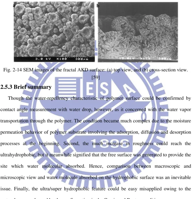
Fig. 2-14 SEM images of the fractal AKD surface: (a) top view, and (b) cross-section view……….22
Fig. 3-1 The chemical structure of PET………..23
Fig. 3-2 The chemical structure of TFA……….23
Fig. 3-3 Dimension of the regular pattern with circle shape………26
Fig. 3-4 Principle of the reversal lithography………..27
Fig. 3-5 The schematic description of the contact angle………...28
Fig. 3-6 The XPS system………...29
Fig. 3-7 The principle of photoelectron generation………...29
Fig. 3-8 Schematic diagram of quartz crystal………31
Fig. 3-9 Schematic diagram of QCM system for moisture uptake measurement……….33
Fig. 3-10 Schematic diagram of a home-built WVTR system………..34
Fig. 4-1 Comparison of contact angle between the (a) untreated PET, and (b) 60W 5 minutes CF4 plasma treatment………36
Fig. 4-2 The relation between plasma treatment time and contact angle………..37
Fig. 4-4 The variation in surface roughness as a function of treatment time………38 Fig. 4-5 The C 1s spectra of (a)untreated PET(b) CF4 plasma treated PET with 60w for
5min……….40 Fig. 4-6 The O 1s spectra of (a) untreated PET (b) CF4 plasma treated PET with 60w for
5min……….40 Fig. 4-7 The moisture absorption of untreated PET and CF4 plasma treatment
for 15 min……….44 Fig. 4-8 Dependence of the moisture uptake and plasma treatment time……….44 Fig. 4-9 The transient curve and the fitting curve of untreated PET………45 Fig. 4-10 The transient curve and the fitting curve of CF4 plasma modified PET for 15
min treatment………..45 Fig. 4-11 The variation of diffusion constant for different treatment time………46 Fig. 4-12 Water vapor permeation rate measurement of untreated PET compared with the
moisture ingress from O-ring………..47 Fig. 4-13 Water vapor permeation rate measurement of untreated PET film and CF4
plasma treated-PET films………47 Fig. 4-14 Variation of thickness and etching time for photoresist………50 Fig. 4-15 Dependence of thickness and etching time for PET……….51 Fig. 4-16 The configurations of the regular pattern without O2 plasma etching (a) top
view for large area,(b) the diameter of circular pattern, and (c) bird's-eye view..52 Fig. 4-17 The configurations of the regular pattern with O2 plasma etching for
700 seconds with (a) bird's-eye view, and (b) the cross-section view…………..53 Fig. 4-18 Contact angle measurement of the fluorinated regular pattern……….55 Fig. 4-19 Water vapor permeation rate measurement of fluorinated regular pattern and flat surface………56
Chapter 1 Introduction
1.1 Background
Due to the necessities of the light weight, smaller size, high mobility, and low cost in flexible device, polymer material was an excellent candidate to meet the desired requirements. However, the broad adoption of polymer substrate would be hindered by high water vapor transmission rate (WVTR) because the organic and electrode matter’s utilized in flexible device was sensitive to moisture. For example, shelf lifetimes of several thousands of hours, for inorganic solar cells packaged with flexible films with WVTR in the range of 1~10-3
g/m2-day. [1] Much strictly in organic light emitting devices (OLEDs), the WVTR should be
lower than 10-6 g/m2-day. Although several approaches had been figured out such as the
addition of inorganic barrier layer on polymer substrate to deduce the WVTR, this limit was the result of permeation through defects or nano-scale pores rather than the bulk of the barrier film. [2, 3] Afterwards, an alternating layer comprised of polymer and ceramic film deposited in vacuum called BarrixTM was developed to achieve the requirement of WVTR for OLED’s applications. [4,5] The cost and thermo-mechanical integrity of such multiple-layer structure remained an inevitable issue. Moreover, instead of improving the steady state permeation rate, multiple barrier layers only extended the diffusion path of the moisture. [6]
Surface modification has technological applications in various fields such as microelectronics, biomaterials, textile, packing, etc. [7] Exposing the polymer surface to plasma can lead to the change of surface chemistry and hence the wettability. Fluorination of polymer with CF4 plasma treatment studied by literature researches showed high
water-repellency characteristic on the polymer surface. [8, 9] However, little has been done to study the water vapor permeation behavior of polymer involving the adsorption, diffusion and desorption of moisture and their impact in the improvement of WVTR polymer after CF4
Ultra/superhydrophobic feature have gained lots of attention due to the extremely high water-repellency characteristic, self-clean (or contamination-free) surface, and applications in micro/nanoelectromechanical system. [10, 11] Because ultra/superhydrophobic feature can’t be generated by surface chemistry alone, it’s well known that the roughness of a hydrophobic solid enhances its hydrophobicity. [12] As the size of water molecular was shrunken from the water drop to water vapor, the dependence of high water-repellency surface and WVTR for polymer substrate was still indistinct. Hence, the other of objectives in the thesis is to design a method to fabricate an ultrahydrophobic surface and discuss whether the enhancement in hydrophobicity could directly affect the WVTR.
The water-repellency of hydrophobic surface inspired us to apply such characteristic to the improvement of WVTR. Among the polymer material, polyethylene terephthalate (PET) had advantages with regarded to clarity, coefficient of thermal expansion (CTE), chemical resistance was selected to be the polymer substrate in the research. [13] CF4 plasma treatment
was adopted to achieve the fluorination of PET. Calcium corrosion test named as “Ca test” helped us to evaluate the WVTR. The condition became much complicated due to the compound process of water moisture permeated through the polymer matrix. Hence, fundamental observation of the surface properties after CF4 plasma modification of PET
should be taken into account in the beginning. There was no exception to study the mechanism of the fluorination on PET which would make the discussion well-organized. To broaden the scope of the research, we introduced the lithography process to fabricate regular pattern. Due to the roughness factor effect, PET was expected to emerge higher hydrophobicity. Finally, the WVTR of the fluorinated regular pattern would be examined by Ca test also.
1.2 Overview
1, Chapter 2 reviewed the degradation of flexible device caused by water vapor, factors controlling the moisture permeation in polymer, fluorination of polymer, and the hydrophobic characteristic. Chapter 3 described the sample preparation, instrumentation and the procedure of lithography process executed in this study. Chapter 4 revealed the comprehensive observation on the fluorination of PET from the wetting properties to chemical composition at first. Then the WVTR of fluorinated was examined by Ca test. The final section was the fabrication and WVTR of fluorinated regular pattern. Then key results and conclusion of this thesis were summarized in Chapter 5.
Chapter 2 Literature review
2.1 Polymer substrate on flexible device
2.1.1 Polymer film as flexible substrates compared with other flexible thin
film.
According to the iSuppli Flexible Display Report, market prospects for flexible displays from 2007 to 2013 showed an explosive development. [13] Polymers were very promising materials for flexible device due to their advantages such as light weight, smaller size, transparency, and low cost. Comparing with the rigid glass which was very difficult to use in a flexible display, polymer had mechanical properties that varied from strong rigidity, such as in engineering plastics, to softness, such as in rubber or polyethylene films. Polymer substrates were some of the least expensive materials and were suitable for mass production via roll-to-roll (RTR)processes. Therefore, they were being considered as the key materials for flexible displays in various application areas including transparent substrates, electrodes, and active materials for light emitting devices (LED), organic light emitting devices (OLEDs), flexible Solar Cell [14], TFT-LCDs and organic thin-film transistors (OTFTs) [15]. Samsung Electronics introduced large area (5 inches) full color transmissive a-Si TFT-LCDs with a resolution of 400×3×300 lines (100 ppi). All the processes of TFT, color filter, and LC were carried out below 150 °C on PES films. [16]
Though the stainless steel foil and ultrathin glass were also considered to be the candidates as the flexible substrates, however, steel foil was hard to handle multiple bends and the weight of stainless steel foil was too heavy to fabricate big size products while ultrathin glass had been limited by its flexibility in use. Moreover, glass substrates were not suitable for some specific applications such as electronic maps and smart cards. The issues of flexibility, weight, and safety were important in glass substrates because glass substrates were very brittle and could not be easily deformed. Therefore, the unique characteristics of polymer
substrate broaden the applications of flexible displays.
2.1.2 Demanded properties of Polymer substrates
Polyimides (PI), polyethersulfone(PES), polyethylene terephthalate(PET) and polyethylene naphthalate (PEN) were commonly used on flexible device. The individual properties of various polymer materials were arranged in table 2-1 and 2-2. To replace glass, a plastic substrate needed to mimic the properties of glass, including its low water vapor transmission rate (WVTR), dimensional stability, thermal stability, solvent resistance, low CTE, and smooth surface, as well as possess good optical properties. Among these properties, low WVTR was the most difficult objective to achieve owing to the native feature of polymer substrate. The WVTR of typical polymer substrates were listed in Table 2-3[17] and the value were much higher than the limitation of flexible devices. Take flexible thin-film transistors
(TFTs) for instance, the WVTR requirementswere generally in the range of 1x10⁻³ g/m2/day to 1x10⁻¹ g/m2/day [3]. Moisture ingressed into the flexible device would cause the loss of
electric performance and the reliability issues. The detail mechanism of moisture degradation would be discussed in next section.
Table 2-1 Comparison of typical polymeric films as plastic substrate. [13]
Table 2-2 Properties of typical polymeric films as plastic substrates. [17]
2.2 Moisture degradation on flexible devices
2.2.1 Mechanisms of moisture degradation on flexible devices.
Since the polymer material had been applied on the flexible device, the innate drawback of high water vapor permeation rate (WVTR) was a main obstruct which would decrease its value from the application view. Whether the application was in displays, lighting, integrated circuits, or photovoltaics, there were materials challenges in implementing flexible and/or organic devices into practical applications. Water vapor, especially, was one of the most important issues which arises the degradation. We would introduced several flexible devices whom water vapor degrade the performance.
2.2.1.1 Moisture degradation on organic thin-film transistors (OTFTs)
There had been a lot of interests in the development of OTFTs in which organic semiconductors were used as active layers because the organic semiconductors were deposited at a low temperature or processed through low-cost solution processes such as spin coating or ink jet printing. Compared to amorphous silicon processes or low-temperature polycrystalline silicon processes, low fabrication temperature of OTFTs allowed a wide range of substrate possibilities and makes an attractive technology for many low-cost electronics applications, particularly those that required or may benefit from flexible polymeric substrates such as rf identification tags, smart cards, electronic paper, and flat panel displays. [19,20]
On the other hand, organic devices also had some significant shortcomings, such as relative low mobility and performance degradation due to moisture and oxygen. D. Li et al. study the effect of humidity on OTFTs performance with p-channel organic semiconductor materials used as active layers. [21] For many OTFT-related applications, such as displays and circuits, the OTFTs should have a high saturation current, field-effect mobility, and ION/
IOFF ratio, and a low threshold voltage and off current. From Fig. 2-2, it could be clearly seen
decreased with increasing RH. Polar water molecules residing at the grain boundaries interacted with hole charge carriers, reducing charge carrier mobility. Another common trend observed was that both the threshold voltage and off-current increase with RH. These results indicated that high WVTR of polymer substrate will effect the performance on OTFT devices which was necessary be faced up to.
Fig. 2-2 Changes of OTFT electrical properties with respect to (RH): (1) (inset) Field-effect mobility[■], saturation current [●], and on/off current ratio[▲]; and (2) threshold voltage [■] and off current [▲].
2.2.1.2 Moisture degradation on solar cell
To combat the environmental problems, solar cells had been in the limelight as a clean energy source. Fig. 2-3 was a real case which polymer substrate applied on the solar cell constructed by H. Nishiwaki et al. with polyimide film. [22] Moisture usually induced the reliability problem in solar cell modules device. Fig. 2-4 shows moisture-induced corrosion that caused gridline adhesion to the silicon cell to fail cause by moisture permeation through the edge of module laminate. [23] Similar phenomena observed by E. E. van Dyk et al, and the damage exhibited in Fig. 2-5 is due to the delamination between the solar cell structures resulting in moisture ingress and corrosion. [24]
organic materials and metal electrode materials such as aluminum were susceptible to reactions with oxygen and water schematically illustrated in Fig 2-6. [25] G. Dennler et al. [26] demonstrated that their device constructed on simple PET film provided a shelf lifetime of less than 6 h. After the water permeation barrier material was added, thelifetime exceeded 3000 h as shown in Fig. 2-7.
Fig. 2-3 Structure of a-Si solar cell with polymer substrate. [21]
Fig. 2-4 Moisture-induced corrosion that caused gridline adhesion to the silicon cell to fail. [22]
Fig. 2-6 Cross section view of a solar cell with the many processes that conspired to degrade organic solar cells. [24]
Fig. 2-7 Normalized circuit current (ISC) and efficiency of solar cells encapsulated with
uncoated PET (■) and with flexible gas barrier material ( ). [25]
2.2.1.3 Moisture degradation on organic light-emitting-diode (OLED)
OLED had fast response time(~1µs), wide view angle (>170°), excellent contrast ratio, brightness, low operating voltage (3-10V) and potentially less power consumption compared to those of LCD or LED. [27] However, The water vapor permeation rate (WVTR) should be lower than 10-6 g/m2-day which was sensitive than 10000 times in LCD shown in Fig. 2-8. [28]
M. Schaer et al. [29] presented the moisture degradation as illustrated in Fig. 2-9. Moisture entered from the defects, such as cracks, pinhole etc. and diffused to the cathode/organic interface. When the device was working, moisture was then reduced at the cathode and yielded hydrogen gas. Then, the bubbles were formed by the evolving hydrogen gas and the organic/electrode interfaces were separated. The electrochemical reduction was:
2H2O+2e-→H2+2OH- (2-1)
Fig. 2-8 Requirements of WVTR and OTR for different applications. [27]
Fig. 2-9 Mechanism of dark spots formation during operation under water vapor environment.[28]
2.2.2 The current methods on prevention the moisture ingress
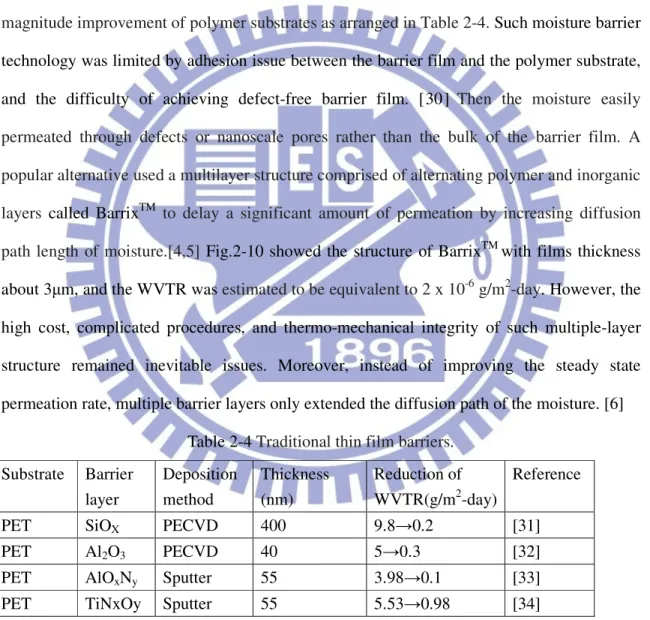
To reduce the impact of moisture degradation and reliability issues while maintaining the
advantage of polymer such as low cost, softness and light weight, thin film barrier was incorporated with the polymer substrate. Thin film barrier usually deposited by plasma-enhanced chemical vapor deposition (PECVD), sputtering, atomic layer deposition (ALD). Traditional thin film single barrier layers provided at best only two to three orders of magnitude improvement of polymer substrates as arranged in Table 2-4. Such moisture barrier technology was limited by adhesion issue between the barrier film and the polymer substrate, and the difficulty of achieving defect-free barrier film. [30] Then the moisture easily permeated through defects or nanoscale pores rather than the bulk of the barrier film. A popular alternative used a multilayer structure comprised of alternating polymer and inorganic layers called BarrixTM to delay a significant amount of permeation by increasing diffusion path length of moisture.[4,5] Fig.2-10 showed the structure of BarrixTM with films thickness
about 3µm, and the WVTR was estimated to be equivalent to 2 x 10⁻⁶ g/m2-day. However, the
high cost, complicated procedures, and thermo-mechanical integrity of such multiple-layer structure remained inevitable issues. Moreover, instead of improving the steady state permeation rate, multiple barrier layers only extended the diffusion path of the moisture. [6]
Table 2-4 Traditional thin film barriers.
Substrate Barrier layer Deposition method Thickness (nm) Reduction of WVTR(g/m2-day) Reference
PET SiOX PECVD 400 9.8→0.2 [31]
PET Al2O3 PECVD 40 5→0.3 [32]
PET AlOxNy Sputter 55 3.98→0.1 [33]
Fig. 2-10 Organic/inorganic multilayer structure from BarrixTM Systems.[4,5]
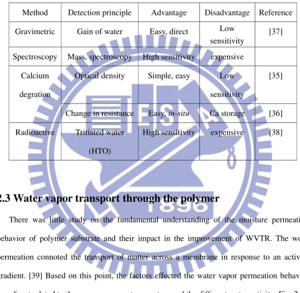
2.2.3 WVTR measurement tool
There were many methods for measuring WVTR which had been developed in the past few years. These methods and their detection principles were summarized in Table 2-5, along with their merits and disadvantage. In addition to the commercial instrument developed by MOCON Inc., calcium degradation test named as “Ca test” was most commonly used in research. The important chemical reactions of calcium with moisture are listed as following:
2Ca+H2O→2CaO (2-2)
CaO+H2O→Ca(OH)2 (2-3)
Assuming a homogenous corrosion occurs when the moisture ingress through the tested sample to the calcium surface, calcium would convert to a transparent oxide or hydroxide salt. The derivative detection principles from the calcium test were optical and electrical approaches. By observing the optical transmittance of calcium layer, one could evaluate the remaining thickness of calcium layer. [35] Ca was a reactive material with water and also a conductive metal. The remaining of calcium height could be obtained by measuring the resistance of calcium described as Eq. 2-4. The WVTR was then calculated using the change rate of resistance according to Eq. 2-5. [36]
bh l
[
]
[ ]
t h h R R Ca M O H M WVTR=δ 2 2 (1− i) i24 (2-5)Table 2-5 Summary of WVTR measuring methods, their detection principles, advantages, and disadvantage.
Method Detection principle Advantage Disadvantage Reference Gravimetric Gain of water Easy, direct Low
sensitivity [37] Spectroscopy Mass, spectroscopy High sensitivity expensive
Optical density Simple, easy Low sensitivity
[35] Calcium
degration
Change in resistance Easy, in-situ Ca storage [36] Radioactive Tritiated water
(HTO)
High sensitivity expensive [38]
2.3 Water vapor transport through the polymer
There was little study on the fundamental understanding of the moisture permeation behavior of polymer substrate and their impact in the improvement of WVTR. The word permeation connoted the transport of matter across a membrane in response to an activity gradient. [39] Based on this point, the factors effected the water vapor permeation behavior was direct related to the vapor pressure, temperature and the different water activity. Fig. 2-11 was revealed by T. Shigetomi et al. [40] showed the relationship between absorbed moister concentration and water vapor pressure. Under the same vapor pressure, the absorbed moister concentration proportion to the environment temperature just as shown in Fig. 2-12.
Fig. 2-11 Sorption-rate curve for water vapor in PET film at different pressure. [40]
Fig. 2-12 Sorption isotherms for water vapor in PET film at different temperature. [40] The penetrant transported in such polymer membranes (without pores、micro-crack) was though to be of the activated-diffusion type; that was, a process in which the gas dissolved in the film at one surface, then migrated through the film under a concentration gradient and desorbed or evaporated from the surface at the lower concentration. From this view, the chemical affinity and its role in transport phenomena should be taken into account. The affinity –∆µ is given by –∆µ
[ ]
[ ]
= l p P P RTln (2-6)T:temperature in Kelvins
[P]l: the concentrations of the penetrant in the vapor phase
[P]p: the concentrations of the penetrant in polymer solid
When the concentration of the penetrant was located in the surface of the solid, the relationship between [P]p and [P]l became the adsorption isotherm. On the other hand for the
case when penetrant molecule in the gas phase [P]l should be changed to the concentration of
the penetrant in the gas phase (partial pressure, denoted as [P]g). Then, in the case of penetrant
transported from the gas phase to a polymer solid, the driving force was regarded to be the transmembrane pressure originating from the difference in concentration of the penetrant between the two sides of a membrane. This type of permeation was called the dissolution/diffusion mechanism. The solubility coefficient” k” was defined by
[ ]
[ ]
g P p P =k (2-7) For the fixed environment conditions such as vapor pressure and temperature, the chemical affinity of the polymer surface would affect the water vapor permeation coefficient P as follows:P≡Dk (2-8)
Where D:the diffusion constant
k: the solubility coefficient
2.4 Fluorination on polymer
From the scope of the factors affected the water vapor transport through the polymer involving the adsorption, diffusion and desorption process, the increase in the water-repellency of polymer surface was seemed a effective way to decrease the WVTR of polymer. Fluorination of polymer surface had been demonstrated to exhibit a good water-repellency characteristic. [8] The following introductions were the methods often
applied on fluorination of polymer surface.
2.4.1 Direct fluorination on polymer
The term “direct fluorination” commonly mean the process of heterogenous reaction of gaseous molecular fluorine or its gaseous mixtures (with N2, He, Ar, O2 and others) with the
polymer surface. [ 41 ] Owing to the high reactivity of fluorine gas, such process is spontaneous at room temperature, proceeded with acceptable rate and no need of heating. This method was widely studied since 80th of 20 century for improving the barrier properties of polymer fuel tanks of vehicles. Furthermore, A. P. Kharitonova et al. had applied the direct fluorination on the commonly used polymer material. [ 42 , 43 ] There were several modification procedures of direct fluorination: [44]
1. Fluorination under static conditions. Polymeric goods under the pressure 1~10-1 torr in the
vacuum chamber which was filled with fluorine or fluorine mixtures followed by evacuation of fluorine after the treatment.
2. Fluorination in stream. Fluorine or fluorine mixtures flowed through the vacuum chamber and isolated from the environment to react with polymer goods.
3. Fluorination during the fabrication. To increase the reaction rate, the polymeric goods was heated above room temperature during the blow molding.
At the direct fluorination of the polymers proceeded cleavage of C–H bonds and opening of double C=C bonds, including conjugate ones, with fluorine addition, and disruption of a significant part of C–N and C–Si bond (when exist) followed by adding of fluorine to carbon atom. [41] The outstanding inertness of fluoropolymers was due to the presence of C–F bonds, which were significantly stronger than conventional C–H bonds. [45] Direct fluorination of polymers was a surface modification process: only 0.01 ~ 1 µm thickness of the material was modified and the bulk properties of the starting polymer remain unchanged. Great variety of commercial properties of polymer articles could be improved by direct fluorination: gas separation properties, adhesion and printability, tensile strength of polymer composites,
chemical resistance, bioresistance, etc. [46]
2.4.2 Plasma enhanced fluorination on polymer
Plasma process presented a clean (producing few or not effluents) and to achieve goals as various as singular in terms of specific properties of use. Based on these advantages, they were used today in many fields of the chemistry of materials and in particular for the modification or manufacture of membranes. Depending on the nature of the gaseous precursor and by adjusting the process parameters, it is possible to perform surface modifications (cross-linking, grafting, etching) in order to change surface properties (like roughness, hydrophobicity or adhesion) of conventional polymer membranes, or to prepare inorganic or hybrid thin films with high thermal and chemical stabilities. [ 47 ] Plasma enhanced fluorination on polymer had received caught lots of eyes due to the widely application. The following are the general gaseous precursor used in plasma enhanced fluorination.
2.4.2.1 SF6 plasma
SF6 plasma was the electro-negative plasma: as a matter of fact the large electronegativity
of fluorine resulted in a large attachment cross-section of electrons on fluorine-containing radicals. SF5+ as the major positive ion species, the electron and the positive ion densities for
the typical discharge parameters were in the range 106–107 and 1010–1011 cm-3, respectively. [48] Two different channels was considered to generate the plasma from SF6 gas. One was the
dissociation of SF6 molecules leading to excited fluorine radicals through the process:
e-+SF6→e-+SF5+F*. The second one consisted in the excitation of free fluorine radicals in the
ground state by inelastic electron collisioned through the process: e-+F→e-+F*. [48] The second mechanism was considered to be the dominant one in typical discharge conditions. J. F. Friedrich et al. employed the SF6 plasma to discuss the solvent separation ability of
poIypropylene (PP) and derived that the plasma modification zone was limited to 10-100 nm. [49]
2.4.2.2 CHF3 plasma
In addition to the application of plasma enhanced fluorination, the selective etching of a SiO2 layer over a Si or Si3N4 was another subject when it comes to CHF3 plasma. [50] K. A.
G. Macneil suggested the most extensively formed ions are F- and CF3- corresponding to the
ion-pair reaction CHF3+e-→CF3- +H+ +e-. [51] The absolute densities of CF3-, CF2- and CF
-radical were estimated to be of the order of 1013 cm-3, 1013 cm-3 and 1012 cm-3 as applied RF power and gas pressure set at 150 Walt(W) and few Pascal (Pa) respectively.[52].
2.4.2.3 CF4 plasma
For CF4 plasma, L. J. Overzat et al. had revealed that F- dominated the negative ions while
several dominant such as CF2+, and CF3+ in positive ions. [53] This result indicated the
following reactions were preferred to occur:
CF4+e-→CF3++F-+e
→CF2++2F-+e- (2-9)
It’s well known CF4 plasma could be employed in chemical etching of silicon dioxide in
semiconductor industry. Besides, CF4 plasma was also widely used in modification treatment
due to the simple chemistry. Furthermore, penetration of plasma surface modification on polymer with CF4 plasma was studied by T. Yasuda et al. [54]
2.5 Hydrophobic characteristic and water-repellency
Although the hydrophobic characteristic of polymer surface could be achieved by fluorination, the previous research revealed the contact angle of several fluorinated polymer surface only attained to 100~110° based on plasma enhanced fluorination. [8] As the scope magnified to the ultrahydrophobic feature of polymer surface, the fundamental understanding should be discussed involving the basic theory and methods to fabricate the ultrahydrophobic surface. Finally, we arranged a brief summary to discuss the relation between
ultrahydrophobic surface and WVTR.
2.5.1 Hydrophobic characteristic
2.5.1.1 Theory
The surface hydrophobicity was a popular research topic due to its widespread applications. When it comes to the surface hydrophobicity, R. N. Wenzel [55] discussed the wetting action at solid surfaces which was a thermodynamic process: Wetting replace an area of the solid-air interface by an equal area of solid-liquid interface and was generally also accompanied by an extension of the liquid-air interface. When a drop of water rested on a horizontal solid surface, the difference of specific energy between the solid-air and solid-liquid interface determined the shape of the drop. Suppose that wetted area had the lower specific energy and that therefore the drop tended to spread spontaneously.
2.5.1.2 Ultrahydrophobic surface
It should be apparent that, for identical the same increase in the free liquid area at the upper surface of the drop, a great amount of the actual surface was wetted under it if the surface of the solid was rough than if it was smooth. The relation mathematically expressed by
cos
θW=r×cos
θY (2-10)where θW=apparent contact angle
θY=Young’s contact angle
r = roughness factor = actual surface/geometric surface
If we aimed to fabricate ultrahydrophobic surface (contact angle >120°), we could increase the roughness factor until reached the demanded request. The theory developed by Cassie and Baxter, however, assumed that air was trapped by the asperities so that the drop sits on a composite surface made of air and solid.[56] Fig. 2-13 showed the comparison between the two conditions between Wenzel state and Cassie and Baxter state. The contact angle based on the Cassie and Baxter were described as
cos
θCB=rfcos
θY+f-1 (2-11)where
cos
θCB= apparent contact angler=roughness factor
f=area fraction of the projected wet area
Fig. 2-13 Schematic of roughness-filling by water according to the Wenzel and Cassie –Baxter models.[57]
2.5.2 Fabrication of ultrahydrophobic surface
From the discussion above, artificial ultrahydrophobic surfaces were fabricated by combining rough surface morphology and low-surface-energy coatings. In general, two main approaches had been developed to generate ultrahydrophobic surfaces. One was to increase directly the surface roughness of low-surface-energy material, and the other was to fabricate a suitable surface roughness with certain materials and then to modify the as-prepared surface with low-surface-energy materials. [58] Applying the former method, E. Martines et al. created the silicon nano-pillars by e-beam writer at the beginning, and then the nano-pillars were coated with octadecyltricholorosilaneoctadecyltricholorosilane(OTS). The contact angle measuredon the OTS-coated flat silicon was 114°. However, the maximum value of contact angle was reported 164° with the diameter of nano-pillar 117 nm and height 792 nm. [57] The alkylketene dimmer (AKD) was a kind of wax, whose contact angle on a flat surface was 109°. As the wax formed a fractal surface shown in Fig. 2-14, the surface wettability changed
from hydrophobic to superhydrophobic with a contact angle as large as 174° reported by T. Onda. [59]
Fig. 2-14 SEM images of the fractal AKD surface: (a) top view, and (b) cross-section view. [59]
2.5.3 Brief summary
Though the water-repellency characteristic of polymer surface could be confirmed by contact angle measurement with water drop, however, as it concerned with the water vapor transportation through the polymer. The condition became much complex due to the moisture permeation behavior of polymer substrate involving the adsorption, diffusion and desorption processes at the beginning. Second, the much increase in roughness could reach the ultrahydrophobic, but it meanwhile signified that the free surface was generated to provide the site which water molecular absorbed. Hence, comparison between macroscopic and microscopic view and water molecule absorbed on the hydrophobic surface was an inevitable issue. Finally, the ultra/super hydrophobic feature could be easy misapplied owing to the water drop were braced by the configuration in the Cassie and Baxter condition.
Chapter 3 Experimental
3.1 Sample Preparation
3.1.1 Chemicals
(1) Polyethylene terephthalate (PET) CAS No. 25038-59-9
Free-standing film: product by Nan Ya Plastics Corporation, thickness 120µm. PET particle: product by Nan Ya Plastics Corporation
Fig. 3-1 The chemical structure of PET.
(2) Trifluoroacetic acid (TFA)
CAS No.76-05-1, purity ≥99%, product by Gelest Inc
Fig. 3-2 The chemical structure of TFA.
3.1.2 Preparation of thin PET film
PET thin film of 0.4 µm thickness was prepared by dissolving PET particle in
trifluoroacetic acid (TFA), and the concentration of the solution is 5 wt%. Before spin coating, the solution was initially filtered through a 0.2 µm PTFE filter (Millipore Inc.) in another bottle. Then we spun the solution onto a (100) silicon wafer at 3000 rpm by spin coater,
followed by baking at 60 oC for 2 hours. The thin film prepared were utilized in the
measurement of quartz crystal microbalance (QCM), (scanning probe microscopy) SPM, n&k analyzer, and X-ray photoelectron spectroscopy (XPS).
3.1.3 Preparation of free-standing film
A free-standing PET thick film with a nominal thickness of 120 µm was cut into 4.5cm×4.5cm. This kind of sample was employed for contact angle and water vapor permeation rate (WVTR) measurement. The PET film was cleaned by acetone, DI water, and then baked at 60 oC for 2 hours. The sample utilized in the WVTR measurement was followed by E-gun evaporation to deposit the Ag with thickness 100 nm, and then the calcium (Ca) was deposited by heat evaporation with thickness 400 nm.
3.2 CF
4Plasma treatment
Plasma was a collection of positive, negative and neutral particles. When an energetic electron struck a neutral reaction gas molecule, it could cause the dissociation to form free radicals, ionization, excitation and radiation. Radicals were chemically reactive and the most important species in the plasma for the surface chemistry. We use the reactive ion etching (RIE) (CRIE-200, AST) to carry out the plasma surface modification. Before plasma treatment, both of the thin film and free-standing films were heated up to 60 in oven for 1 ℃ hour in order to remove absorbed water. The detail parameter of CF4 plasma treatment was
Table 3-1 Experimental conditions for CF4 plasma treatment
Gas Flow rate
(sccm)
Pressure (mtorr) Power (W) Time (min)
20 70 60 5
20 70 60 10
CF4
20 70 60 15
3.3 Fabrication of regular pattern
The approach to fabricate the regular pattern in this study was based on lithography process which also widely used in semiconductor industry. Owing to the complicated process during the lithography process, we detached the fabrication of regular pattern into an independent section. The procedure was listed as following:
3.3.1 Sample preparation and instrument
A 45×45 mm2 PET film of thickness of 120 µm was prepared at the beginning. Before the
lithography process, PET film was cleaned by acetone, DI water, and then baked at 60 oC for 2 hours. The dimension and shape of the pattern on the mask was shown in Fig. 3-3. Unlike the traditional lithography process, we applied the “reversal lithography” technology in this study illustrated in Fig. 3-4. We used the photoresist called AZ® 5214 E invented by MicroChemicals [60]. It’s a very special photoresist which was capable of image reversal. Exposed areas may be selectively cross-linked by applying a bake cycle after exposure. A flood exposure before development converted unexposed areas soluble, resulting in a negative tone image. Mask aligner exposure (Karl-Suss MJB-3) equipped mercury (Hg) light source with wavelength 350nm~450nm was put into use. FH-D5 was designated as developer while the DI water as fixer.
3.3.2 Procedure
1. Photoresist was deposited by spin-coater at 2000 r.p.m. then baked at 90℃ for 2 minutes. 2. Exposing the photoresist with mask aligner exposure for 27 seconds, and we could define
the area of pattern.
3. The phoresist was cross-linked by applying a bake cycle after exposure at 120℃ for 2 minutes, and then a flood exposure was executed for 27 seconds.
4. Dipped into the developer and fixer for 30 seconds individually, the photoresist created reversal image.
5. Finally, we applied the RIE system (RIE-200, AST) to etch the photoresist and PET with O2 plasma. The operating pressure and power were adjusted at 55 mtorr and powers of
100W.
Fig. 3-4 Principle of the reversal lithography. [60]
3.4 Analysis instrument
3.4.1 Contact angle (CA) measurement
For the sake of understanding the hydrophobic property, contact angle ,θ , is a quantitative measurement of the wetting of a solid by a liquid. The wetting process can be thought as a thermodynamic equilibrium between the three phases: the liquid phase of the droplet (L), the solid phase of the , and the gas/vapor phase of the ambient (G) which can be describe as equation 3-1. As each interface has its own specific energy content and the shape of the drop is determined by the wetting property of the examined surface. Suppose that the wetted area has the lower specific energy and that therefore the drop tend to spread to take place the original one. The net energy continuous decreases until reach the thermodynamic equilibrium.
γ
SG=γ
LG*cosθ
C+γ
SL(
3-1) The contact angle was obtained by contact angle measurement instrument (First Ten Angstroms FTA125) with accuracy 0.1°, and the operation environment was under atmosphere and room temperature.Fig. 3-5 The schematic description of the contact angle
3.4.2 X-ray Photoelectron Spectroscopy (XPS)
The fundamental principle of X-ray Photoelectron Spectroscopy (XPS) was optoelectronic effect and used X-ray beam to illuminate static solid surface that could be ionized to scatter photoelectron [61]. The instrument was schematic illustrated in Fig. 3-6. The energy of a photon of all types of electromagnetic radiation is given by the Einstein relation:
Ee h s
E(1 )= ν−
(
3-2) Where E( s1 ): binding energy in 1s orbitν
h : the energy of x-ray or UV Ee: the energy of photoelectron
When the atomic was illuminated by X-ray, X-ray energy was larger than the electron binding energy of the inside layer L orbit, electron could be ionized to be free electron that was called photoelectron show as Fig. 3-7 For each and every element, there will be a characteristic binding energy associated with each core atomic orbital i.e. each element will give rise to a characteristic set of peaks in the photoelectron spectrum at kinetic energies determined by the photon energy and the respective binding energies. The presence of peaks at particular energies therefore indicates the presence of a specific element in the sample under study. Furthermore, the intensity of the peaks is related to the concentration of the
element within the sampled region. Thus, the technique provides a quantitative analysis of the surface composition
The composition and chemical bonding of the PET after CF4 plasma treatment was
investigated using XPS (ULVAC-PHI, PHI Quantera SXM2). The photoelectron emission spectra were obtained using an Al X-ray source (1486.6eV) striking the surface of the sample. The analyzer resolution was fixed at 0.01 eV and the detected depth within 50 Å.
Fig. 3-6 The XPS system.
K L M N X-ray or UV photoelectron K L M N X-ray or UV photoelectron
3.4.3 X-ray Reflectivity (XRR)
XRR now had become a widely used tool for the characterization of thin-film and multilayer structures. X-ray scattering at very small diffraction angles allowed characterization of the electron density profiles of thin films down to a few tens of angstroms. Using a simulation or the least-squared fit of the reflectivity pattern, one could obtain highly accurate measurements of thickness, interface roughness, and layer density for multilayer thin film. XRR measurement used a series θ-2θ scanning, that is, an incident light move around the sample within an extremely small angle θ and a detector move 2θ angle simultaneously to receive the signal. [62] XRR was employed to examine the surface density variation of PET films after various CF4 plasma treatments using beam-line 13A1 of National Synchrotron
Radiation Research Center (NSRRC) in Hsinchu, Taiwan. The test condition was keep at room temperature and one atmosphere while the incident angle varied from 0 to 2.5 degree.
3.4.4 Quartz Crystal Microbalance (QCM)
To understand the variation of water vapor absorption and diffusion behavior of modified
PET, a home-built QCM was employed tomeasure moisture uptake of fluorinated PET films. QCM was an extremely sensitive tool down to nano-gram level due to the application of piezoelectric effect. The quartz crystal would deform and had a specific resonant frequency while AC electronic filed was applied to quartz crystal. According to Sauerbrey equation [63], the mass load on crystal could be calculated by the measured resonant frequency.
3.4.4.1 Sauerbrey Equation
For a quartz crystal plate to oscillate in thickness shear mode, the following equation must be satisfied:
2
q
tq= λ (1) where
λq : wavelength of shear-mode elastic wave
Fig. 3-8 Schematic diagram of quartz crystal
Speed of acoustic wave in the same material was a constant and could be described by the following equation: 2 1 = q q v ρ µ (2) ν: wave speed
µq : the shear modulus of crystal ρq : the density of crystal If ν=f0 λ substitute into (1), then
tq f 2 0 ν = (3)
Assume a thin layer with thickness, △t, was absorbed, then
t tq q ∆ + = 2 λ
After adsorbed, wavelength became longer and wave speed would not change, we can get following equation: tq t f =−∆ ∆ (4) Substitution of (3) into (4) 2 1 0 0 0 ∆ − = − = ∆ q q t f f f f ρ µ ν (5)
q t A m= ∆ρ
∆ (6)
A : piezoelectric active area △m : mass of adsorbs Substitution of (6) into (5) ∆ − = ∆ 2 0 2 f f A m ρqµq ……… (3-3) where
µq: the shear modulus of crystal(2.947×10¹¹ g.cm-1.sec-2 )
ρq: the density of crystal (~2.648 g.cm3) A: piezoelectric active area
△f: Frequency change before and after adsorption △m: Mass loading
3.4.4.2 Quartz crystal microbalance (QCM) system
A home-built quartz crystal microbalance system, schematically illustrated in Fig. 3-9, consisting of vacuum chamber, oscillator, frequency counter (HP 53131A), temperature controller, water vapor bubbler and computer-controlled data collection system, was used in this thesis. The AT-cut quartz crystal with 9 MHz resonant frequency (Mercury Electronics. Inc.) had a diameter and thickness of 0.8 cm and 200µm, respectively. Diameter of active Au electrode was 0.4 cm. The measurement of moisture uptake was carried out under 100% relative humidity at 25 oC. The sensitivity of our QCM using a 9 MHz AT-cut quartz crystal is
1.72 ng/cm2 based on the 1 Hz resolution of HP frequency counter according to Sauerbrey equation.
oscillator Frequency
counter computer IEEE488GBIP
Vacuum pump Vapor source
Temperature controller
Fig. 3-9 Schematic diagram of QCM system for moisture uptake measurement
3.4.5 Ca corrosion test
Ca degradation test was commonly utilized to measure the water vapor transmission rate (WVTR) which was often named as the “Ca test”. [35, 36] This method was based on the corrosion of calcium films and subjected at a fixed temperature and humidity. A home built Ca test system whose detection limit is 5x10⁻⁵g/m2/day as exhibit in Fig. 3-10 and the experimental temperature was keep at 25℃ and 100 % relative humidity (RH) condition. The fabrication of Ca sensor follows the following sequences. A 100 nm silver film was deposited by e-gun evaporated on the flexible PET film (45 mm × 45 mm size, 125 µm thick) to serve as the four-point probe electrodes. Then, calcium layer of 400 nm was deposited by evaporation deposition as the detection layer for moisture reaction. The important chemical reactions of calcium with moisture are listed as following:
2Ca+H2O→2CaO (3-4)
Assuming a homogenous corrosion occurs when the moisture ingress through PET film to the calcium surface, the resistance of remaining Ca layer is measured in-situ by a four point probe method and LabVIEW software, and is expressed by
and is expressed by Eq. (3-6)
bh
l
R
=
ρ
(3-6)where ρ denotes the Ca resistivity, l is the length and b is the width of the Ca layer, and h is the thickness of the calcium film. The water vapor permeation rate, P is then calculated using the change rate of resistance according to Eq. 3-7 [36].
[
]
[ ]
t h h R R Ca M O H M WVTR=δ 2 2 (1− i) i24 (3-7)where h denotes the Ca height, R is the resistance of the thin Ca layer connected to the electrodes, δ is the Ca density, and M is the molar mass of the indicated reagent. Ri and hi are initial values of R and h.
Moisture Chamber Te mp era ture Co ntr olle r P um p HP multimeter Vapor source LabVIEW PET LiF layer Ca layer Ag Ag Moisture Chamber Te mp era ture Co ntr olle r P um p HP multimeter Vapor source LabVIEW PET LiF layer Ca layer Ag Ag Moisture Chamber Te mp era ture Co ntr olle r P um p HP multimeter Vapor source LabVIEW PET LiF layer Ca layer Ag Ag
3.4.6 Scanning probe microscope (SPM)
SPM (Veeco Dimension 5000) was utilized to study the surface morphology and the roughness of PET after the CF4 plasma treatment. The scanning boundary was 5×5 µm2 and
the deviation of roughness was below 0.5 angstrom (A). The operation was carried out at room temperature and one atmosphere.
3.4.7 FE-SEM
Field-emission scanning electro spectroscopy (FE-SEM) (JEOL 6700F) was employed to investigate the morphology of regular pattern. The operation pressure was under 9.86×10⁻⁵ torr and the emission current was set at 10µA.
3.4.8 n&k analyzer
The n&k analyzer 1200 in National Nano Device Laboratory (NDL) was used in this study to obtain the varied thickness of photo-resist and PET by O2 plasma etching during the
fabrication of regular pattern. The experimental steps were listed below:
1. To scan standard sample as a baseline. (The wavelength ranged from 190 nm to 900 nm.) 2. To put sample wafer upside down on the n&k analyzer, and then scan again to collect the
typical experimental curve.
The experimental curve was fitted using Forouhi-Boomer Dispersion relation [64] to deduce the film thickness. The goodness of fit was all above 99% for the entire sample.
Chapter 4 Results and Discussion
4.1 Characteristics of fluorination on PET
4.1.1 Wetting property and morphology of fluorinated PET.
Hydrophobicity was the index to determine the wetting property, and the evaluation of hydrophobicity could be made through water contact angle measurements. The original contact angle of PET utilized in this thesis was about 64.5° while a significant increment to 107.7° after CF4 plasma treatment for 5 minutes at power 60W which indicated the surface
became hydrophobic (contact angle>90°) as shown in Fig. 4-1. To understand the dependence of treatment time and hydrophobic characteristic, we extended treatment time was performed from 5 to 15 minutes. Fig. 4-2 shown the contact angle versus different treatment time, the value seemed to be saturated at 106~107°. This result indicated that the PET surface with treatment time within 15 minutes had the same hydrophobicity.
Fig. 4-1 Comparison of contact angle between the (a) untreated PET, and (b) 60W 5 minutes CF4 plasma treatment.
0 5 10 15 60 70 80 90 100 110 120 c o n ta c t a n g le (d e g re e )
treatment time (min)
Fig. 4-2 The relation between plasma treatment time and contact angle.
To learn more about the morphology of CF4 plasma modified PET, the scanning probe
microscopy (SPM) had been then used in this work by evaluating the surface area 5×5 µm2. Fig. 4-3 showed the surface morphology of untreated PET with height scale 20 nm and the roughness was only 0.34 nm. The roughness increased to 1.01 nm after CF4 plasma
treatment for 15 minutes at power 60W. The variation in surface roughness of treated PET as a function of treatment time was exhibited in Fig. 4-4. Revealed by literature studies, the CF4
plasma modification was described as the sum of two mechanisms: ion etching and fluorination, and the two reactions seemed to be competitive and parallel. The ion etching action had been suggested to be mostly due to ion bombardment which will roughen the surface. [65]
Fig. 4-3(a) The surface roughness of untreated PET, and (b) 15 minutes treatment.
0 5 10 15 0.2 0.4 0.6 0.8 1.0 s u rf a c e r o u g h n e s s (n m ) treatment time(min)
Fig. 4-4 The variation in surface roughness as a function of treatment time.
As mention in previous chapter, contact angle would be affected with roughness factor. However, this phenomenon didn’t appeal in our case because the increment of surface roughness was only 0.67 nm. The slight increase in roughness may attribute to the pure CF4 as
the gas source. Several researches concluded that the addition of other gas source will enhance the ion etching process. [66, 67]
4.1.2 Chemical structure and depth of plasma fluorination zone
The chemical structure of plasma fluorinated PET was justified by the resolution of the X-ray Photoelectron Spectroscopy (XPS) spectra. Typically the XPS spectra of PET C 1s had three main peaks shown in Fig. 4-5 and table 4.1.1 C–C/C–H at 284.6eV, C–O at 286.4 eV, O=C at 288.7 eV. After CF4 plasma treatment for 60w 5min, there was a dramatic change
exhibited on the XPS spectra which could be attributed to formation of fluorinate carbon functionalities: CF at 289.3 eV, CF2 at 291.1 eV and CF3 at 293.1 eV.[68,69] These results
indicated that both the C-C、C-H and C=O group were all likely effected by fluorination. As shown in O (1s) spectra in Fig 4-6 and table 4-2, C=O bond at decreased in the proportion while C-O bond increased relatively. An extra peak at 534.7 eV was assigned as C(O)F. This
![Fig. 2-2 Changes of OTFT electrical properties with respect to (RH): (1) (inset) Field-effect mobility[■], saturation current [●], and on/off current ratio[▲]; and (2) threshold voltage [■] and off current [▲]](https://thumb-ap.123doks.com/thumbv2/9libinfo/7517178.118303/19.918.158.802.302.757/changes-electrical-properties-respect-mobility-saturation-threshold-voltage.webp)
![Fig. 2-3 Structure of a-Si solar cell with polymer substrate. [21]](https://thumb-ap.123doks.com/thumbv2/9libinfo/7517178.118303/20.918.191.726.308.794/fig-structure-si-solar-cell-polymer-substrate.webp)
![Fig. 2-8 Requirements of WVTR and OTR for different applications. [27]](https://thumb-ap.123doks.com/thumbv2/9libinfo/7517178.118303/22.918.218.733.337.870/fig-requirements-wvtr-otr-different-applications.webp)
![Fig. 2-11 Sorption-rate curve for water vapor in PET film at different pressure. [40]](https://thumb-ap.123doks.com/thumbv2/9libinfo/7517178.118303/26.918.192.768.115.725/fig-sorption-rate-curve-water-vapor-different-pressure.webp)
![Fig. 2-13 Schematic of roughness-filling by water according to the Wenzel and Cassie –Baxter models.[57]](https://thumb-ap.123doks.com/thumbv2/9libinfo/7517178.118303/32.918.159.799.215.839/schematic-roughness-filling-according-wenzel-cassie-baxter-models.webp)