國 立 交 通 大 學
電子工程學系 電子研究所碩士班
碩 士 論 文
高介電常數材料(HfAlO
x
N
y
)在MOS元
件上特性之研究
Characteristic and Investigation of High-k
(HfAlOxNy) Dielectric on MOS Devices
研
究
生 : 傅文煜
指 導 教 授 : 葉清發 博士
高介電常數材料(HfAlO
xN
y)在MOS元件上特性
之研究
Characteristic and Investigation of High-k (HfAlO
xN
y)
Dielectric on MOS Devices
研 究 生:傅文煜 Student : Wen-Yu Fu
指導教授:葉清發 博士 Advisor
:
Dr.
Ching-Fa
Yeh
國 立 交 通 大 學
電子工程學系 電子研究所碩士班
碩 士 論 文
A Thesis
Submitted to Departent of Engineering & Institute of Electronics
College of Electrical and Computer Engineering
National Chiao Tung University
in Partial Fulfillment of the Requirements
for the Degree of Master
In
Electronics Engineering
July 2006
高介電常數材料(HfAlO
x
N
y
)在MOS元
件上特性之研究
研究生:傅文煜 指導教授:葉清發 博士
羅正忠 博士
國 立 交 通 大 學
電子工程學系 電子研究所碩士班
摘 要
根據半導體的微縮定律,隨著半導體製造逐漸的微小化,極薄的
二氧化矽介電層將伴隨著極大的直接穿遂漏電流,而這個直接穿遂漏
電流將對元件的功率消耗有嚴重的影響。在閘極二氧化矽介電層薄到
10 奈米以下的情況之下,為了解決這嚴重的直接穿遂漏電流現象,
我們將利用高介電係數材料來替換傳統的二氧化矽。我們利用高介電
係數材料在相同的等效二氧化矽厚度之下,能擁有較大的實際物理厚
度以抵擋直接穿遂漏電流。
在眾多高介電係數材料之中,二氧化鉿和三氧化二铝是非常有潛
力的高介電係數材料。二氧化鉿有較高的介電係數,但它的結晶溫度
太低<500oC。為了克服二氧化鉿結晶溫度太低的問題,我們加入三氧
化二铝去改善這問題及提升載子能障.當高介電數材料直接沈積在矽
晶圓表面上時,在介面的地方會有一層二氧化矽的介面層產生.這一
層介面層的品質扮演著非常重要的角色對於在元件的特性和可靠
度.所以我們想要成長一層像熱二氧化矽一般,有很少的介面缺陷特
性的極薄氧化層,來改介面特性和電性.在我們的實驗過程中,在成
沈高介電質之前我們利用紫外光及上臭氧去成長一層高品質的極薄
氧化層.
本論文首先研究以紫外加上臭氧在室溫成長的薄氧化層的基本
特性.從實驗結果,我們發現利用紫外加上臭氧所成長的二氧化矽具
有自我限制的飽和成長特性.接下來討論不同的沈積後退火的溫度在
沈高介電質之前我們利用紫外光及上臭氧去成長一層高品質的極薄
氧化層.介由電性的量得到一個適合的沈積後退火的溫度(900oC
30sec).在第二章最後比較了有做紫外光臭氧表面、沒有做過任合表
面處理及做了紫外光臭氧之後加上 NH3 電漿的氮化的表面處理.從漏
電流密度、遲滯現象、TZBD、等效氧化層厚度的電性觀點來看,
我們發現在沒有做過任合表面處理不管是從漏電流密度、遲滯現象、
TZBD、等效氧化層厚度都不如有做紫外光臭氧的表面處理,而在
做了紫外光臭氧之加 NH3 電漿的氮化的效氧化層厚度下表面處理雖
然等效氧化層厚度下降,但大量的氮合併造成其它電性的衰退,像是
漏電流密度、遲滯現象、TZBD.總合上面的結論來看,我們得到
紫外光臭氧的表處理是最佳的化的條件.
在本論文的最後,利用第二章的最佳化的條件去做成 nMOSFETs 同
時去把沒有做表面處理條件做成 nMOSFETs 來做比較.經由電性上的
結果來看,發現有明顯的改善.最後利用 CVS 去探討可靠度,不管是
從表面缺陷密度的增加量和 Bulk 的缺陷密度的增加量都也有明顯的
改善.而且從結果得知不管是否有經過表面處理,都是 Bulk 的缺陷
密度的增加量為造成臨限電壓偏移的主要原因.
Characteristic and Investigation of High-k
(HfAlO
x
N
y
) Dielectric on MOS Devices
Student:Wen-Yu Fu Advisor : Dr. Chin-Fa Yeh
Dr. Jen-Chung Lou
Department of Electronics Engineering and Institute of Electronics
National Chiao Tung University, Hsinchu, Taiwan
Abstract
According to the scaling rules, aggressive scaling has led to silicon dioxide (SiO2)
gate dielectrics as ultra thin in state-of-the-art CMOS technologies. As a consequence, static leakage power due to direct tunneling through the gate oxide has been increasing at an exponential rate. As technology roadmaps call for sub-10Å gate oxides within the next five years, a variety of alternative high-k materials are being investigated as possible replacements for SiO2. The higher dielectric constants in
these materials allow the use of physically thicker films, potentially reducing the tunneling current while maintaining the gate capacitance needed for scaled device operation.
material. Hafnium oxide has the higher dielectric constant, but it tends to crystallize at a relatively low process temperature (<500oC). In order to overcome this problem, add Al2O3 in HfO2 for improve crystallization temperature and barrier height. There
are many interfacial states as high-k materials directly contact silicon. However, the control of SiO2-like interface between high-κ dielectrics and silicon substrate pays
more and more important, since the device performances and reliability characteristics are strongly affected by the interface quality. Therefore we want to grow like thin thermal SiO2 that have very lower interface state to improve the interfacial layer and
electrical characteristics. In this thesis, the basic properties of the ozone oxide were studied first. A saturated oxidation was observed in the growth curves and the resultant self-limiting property. Then different post deposition anneal is studied on HfAlOxNy gate dielectric prior UV ozone treatment. PDA can effectively improve
gate dielectric quality. Therefore, post deposition anneal must to do but a suitable anneal temperature is very important on electrical characteristics. In this chapter, we find a suitable anneal temperature to improve electrical characteristics. From the hysteresis , leakage density and time zero to breakdown determine the post deposition anneal at 900 oC and that has excellent electrical characteristics. We compared with UV ozone treatment and without on electrical characteristics. We observe that, no matter on EOT, hystersis, leakage current density and TZBD have excellent electrical characteristics. By different NH3 plasma treatment’s time of UV ozone oxide prior to
HfAlOxNy gate dielectric deposition were investigated. We find that NH3 nitridation
would degrade device performance such hystersis, leakage current density and TZBD. Though EOT decreasing with the NH3 treatment‘s time increasing but that
improvement on electrical characteristic is little. We determine the optimum condition (UV ozone surface and post deposition anneal 900oC 30s) by above result.
In the thesis final, we used optimum condition on chapter two to fabricate the nMOSFETs and a control sample (without treatment and PDA900oC 30seconds after high k film deposit) was fabricated at the same time. We can observe that improved electrical characteristics on nMOSFET with UV ozone surface treatment.Then we estimate reliability of the HfAlOxNy stacks nMOSFETs by
constant voltage stress (CVS). We find that UV ozone surface treatment can improved delta interface state density and bulk charge trap density during the constant voltage stress compared with the control sample. We observe that the bulk charge density to dominate the threshold voltage shift charge during the constant voltage stress for with UV ozone treatment and without
誌 謝
在兩年的碩士生涯中,首先我要感謝我的指導教授羅正忠博士和
葉清發博士,由於兩位老師在研究上給予我細心的指導及教誨,讓我
在學術及研究上都有莫大的收穫。更感謝兩位老師在生活上及待人處
事方面給我的幫助及啟發,讓我受益良多並更加成長,在這裡對兩位
老師致上內心最誠摯的敬意與謝意。
此外,我要感謝我的女朋友宛真因為有她在我背默默的支持,在
我實驗失敗的時候給我信心及鼓勵,讓我能順利地完成研究。還有陳
永裕、林柏村、陳世璋、陳旭維、藍文廷…等諸位學長,謝謝你們的
鼓勵及協助,並在我實驗遇到困難的時候,給予我正確的前進方向,
沒有你們的幫助這篇論文是沒辦法順利完成的,謝謝你們。同時,也
要感謝曾經一起同甘共苦的同學們:伯翰、國源、致維、建華、國信、
修豪、佳寧,和你們在一起的二年光陰讓我學習了不少的生活經驗,
也感謝你們豐富了我的生活。另外我要在特別感謝:伯翰,因為你辛
勤的為實驗室付出和熱心的待人,讓我在量測方面能順利的完成及得
到不少專業方面的知識,也要感政凱、彥銘、宏仁、建宏…等等碩一
的學弟妹的協助。其實還有好多好多的人需要感謝,你們陪同我一起
走過了許多的酸、甜、苦、辣,一起釀造了最美好的回憶。我由衷地
感謝你們,並會將你們銘記在心裡的。另外,我要感謝國家奈米元件
實驗室(NDL)與交大半導體中心提供良好的設備與研究環境,讓我能
順利的完成實驗。
最後我要感謝我的家人,我的妹妹傅瑜芳和弟弟傅文俊,一路上
陪我成長及學習,父親傅珍枝和母親張碧華多年來辛苦的栽培與教
誨,提供我自由的成長空間,並給我最大的關懷與支持,使我無後顧
之憂的完成我的碩士學位。在此獻上內心最深的謝意:爸、媽,謝謝
你們~。
Contents
Abstract (Chinese) ... I Abstract(English)...IV Acknowledgements ...VII Contents... XIV Table Captions...XVII Figure Captions ... XVIIIChapter 1
Introduction
1.1 Background...1 1.2 Motivation……….……...3 1.3 Organization of the Dissertation...4
Chapter 2 Comparison of Various Surface Treatment on the HfAlO
xN
yMOS Devices Characteristics
2.1 Introduction ………8 2.2 Experiment Details
2.2.1 Experiment Details of Ozone Oxide Growth………….…9 2.2.2 Different Post Deposition Anneal Characteristics of
HfAlOxNy MOS Devices with Ozone Surface
Treatments………10 2.2.3 UV Ozone Treatment and Without UV Ozone Treatment
Characteristics of HfAlOxNy MOS Devices………...…11
2.2.4 NH3 Plasma Treatment on Ozone Surface Treatment Characteristics Of HfAlOxNy MOS Devices……..……12
2.3 Results and Discussions
2.3.1 Basic Property Investigation of the Ozone Oxide………13 2.3.2 Different Post Deposition Anneal Characteristics of
HfAlOxNy MOS Devices with Ozone Surface
Treatments Effect……….………13 2.3.3 Comparison of UV Ozone Treatment and Without UV
Ozone Treatment Characteristics of HfAlOxNy MOS
Devices………...……..15 2.3.4 Comparison of Different NH3 Plasma Treatment on
Ozone Surface Characteristics Of HfAlOxNy MOS
Devices……….16 2.4 Summary ...18
Chapter 3 HfAlO
xN
yMOS FET Devices Characteristics
3.1 Introduction ……...37 3.2 Experiment Details………38 3.3 Results and Discussion
3.3.1 Basic electrical Properties Of Devices………42 3.3.2 Constant Voltagee Stress………….……….45 3.4 Summary ...46
Chapter 4 Conclusions and Suggestions for Future Work
4.1 Conclusions…...65 4.2 Recommendations for Future Works...67
Table Captions
Chapter 1
Table 1-1. International Technology Roadmap for Semiconductors.
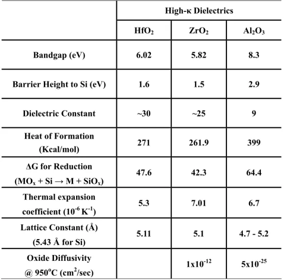
Table 1-2. Materials properties of high-κ dielectrics, Al2O3, ZrO2, and HfO2.
Chapter 2
Chapter 3
Figure Captions
Chapter 1
Figure 1-1 Scaling of MOSFETs. Figure 1-2 High k materials.
Chapter 2
Figure 2-1 UV ozone system schematic diagram. Figure 2-2 Sputter system schematic diagram. Figure 2-3 Cross section and process flow Figure 2-4 Cross section and process flow Figure 2-5 Cross section and the process flow
Figure 2-6 Growing curve of UV ozone oxide UV ozone oxide growing 5min with annealing 900oC 60sec in the nitrogen ambient and without.
Figure 2-7 UV ozone oxide growing 5min with annealing 900oC 60sec in the nitrogen ambient and without.
Figure 2-8 Normalized capacitance-voltage (C-V) characteristics of HfAlOxNy
stacked gate dielectrics with various post deposition anneal on UV ozone treatment samples.
Figure 2-9 Vfb Weibull distribution of HfAlOxNy stacked gate dielectrics with
various post deposition anneal on UV ozone treatment samples. Figure 2-10 The hysteresis of various post deposition anneal on UV ozone
treatment
Figure 2-11 EOT Weibull distribution of HfAlOxNy stacked gate dielectrics with various PDA temperatures on UV ozone treatment samples.
Figure 2-12 Leakage current density of HfAlOxNy stacked gate dielectrics with various PDA temperatures on UV ozone treatment
Figure 2-13 Leakage current density at Vfb-1 distribution of HfAlOxNy stacked
samples.
Figure 2-14 Assembled the EOT and leakage current density at Vfb-1 of HfAlOxNy
stacked gate dielectrics with various PDA temperatures on UV ozone treatment samples.
Figure 2-15 TZBD of HfAlOxNy stacked gate dielectrics with various PDA temperatures on UV ozone treatment samples.
Figure 2-16 Normalized capacitance-voltage (C-V) characteristics of HfAlOxNy
gate dielectric PDA 900oC with ozone surface treatment and without treatment.
Figure 2-17 Vfb Weibull distribution of HfAlOxNygate dielectric PDA 900oC
with ozone surface treatment and without treatment.
Figure 2-18 The hysteresis of UV ozone treatment samples and without.
Figure 2-19 EOT Weibull distribution of HfAlOxNy stacked gate dielectrics with PDA 900oC on UV ozone treatment samples and without zone treatment.
Figure 2-20 Compare with leakage current density of HfAlOxNy stacked gate dielectrics with PDA 900oC on UV ozone treatment samples and without zone treatment.
Figure 2-21 Leakage current density @ Vfb-1 distribution of HfAlOxNy stacked
gate dielectrics with PDA 900oC on UV ozone treatment samples and without zone treatment.
Figure 2-22 The time-zero dielectric breakdown (TZDB) of HfAlOxNy stacked gate dielectrics with PDA 900oC on UV ozone treatment samples and without zone treatment.
Figure 2-23 Normalized capacitance-voltage (C-V) characteristics of HfAlOxNy
gate dielectric PDA 900oC prior to ozone surface treatment follow various NH3 plasma treatment’s times.
Figure 2-24 Vfb Weibull distribution of HfAlOxNygate dielectric PDA 900oC prior
to ozone surface treatment follow various NH3 plasma treatment’s
times.
Figure 2-25 The hysteresis of of HfAlOxNygate dielectric PDA 900oC prior to
ozone surface treatment follow various NH3 plasma treatment’s times.
Figure 2-26 EOT of of HfAlOxNygate dielectric PDA 900oC prior to ozone surface
Figure 2-27 Leakage current density of of HfAlOxNy gate dielectric PDA 900oC
prior to ozone surface treatment follow various NH3 plasma
treatment’s times.
Figure 2-28 Leakage current density @ Vfb-1 distribution of of HfAlOxNygate
dielectric PDA 900oC prior to ozone surface treatment follow various NH3 plasma treatment’s times.
Figure 2-29 The time-zero dielectric breakdown (TZDB) of HfAlOxNygate
dielectric PDA 900oC prior to ozone surface treatment follow various NH3 plasma treatment’s times.
Chapter 3
Figure 3-1 The cross section and the key process flow of nMOS transistor. Figure 3-2 Basic experimental setup of charge pumping measurement.
Figure 3-3 Configuration for (a) gate-to-channel, (b) gate-to-substrate capacitance measurements.
Figure 3-4 Id vs Vd characteristics of UV ozone surface treatment and without treatment VG-Vth= 0 ~ 2 V, step= 0.5 V, W/L=20 μm/8μm.
Figure 3-5 High frequency (100 kHz) C-V characteristic of the HfAlOxNy stacks. EOT are 20 and 20.2 for with and without UV ozone treatment,
respective.
Figure 3-6 Cumulative probability of the threshold (Vth) for HfAlOxNy stacks nMOSFETs.
Figure 3-7 (a) Id vs Vg, (b) Hystersis of nMOSFET characteristics with UV ozone treatment.
Figure 3-8 (a) Id vs Vg, (b) Hystersis of nMOSFET characteristics without UV ozone treatment.
Figure 3-9 Normalized transconductance characteristic of nMOSFET with HfAlOxNy stacks.
Figure 3-10 Mobility characteristic of nMOSFET with HfAlOxNy stacks. Figure 3-11 Leakage current density of nMOSFET with HfAlOxNy stacks. Figure 3-12 Charge pumping measurement (a)Icp (b)Id+Is
Figure 3-13 (a)Weak rise-time dependence of charge pumping current for fixed fall time. (b)Strong fall-time dependence of charge pumping current for fixed rise time. On UV ozone treatment sample.
Figure 3-14 (a)Weak rise-time dependence of charge pumping current for fixed fall time. (b)Strong fall-time dependence of charge pumping current for fixed rise time. On control sample.
Figure 3-15 Basic measurement method for CVS
Figure 3-16 Delta Vthc versus stress time for device with and without UV ozone treatment.
Figure 3-17 Delta Nit versus stress time for device with and without UV ozone treatment.
Figure 3-18 Delta Ntotal versus stress time for device with and without UV ozone treatment.
Figure 3-19 Delta Nbulk versus stress time for device with and without UV ozone treatment.
density versus the stress times with UV ozone treatment.
Figure 3-21 Interface charge densities, bulk charge densities and total charge density versus the stress times without UV ozone treatment.
CHAPTER 1
Introduction
1.1 Background
Recently, information technology (IT) revolution has progressed dramatically, as can be seen in the rapid spread of Internet and cellular phones. The revolution will change significantly our life and culture, and is expected to improve the quality of life. The progress and spread of the IT technology owe much to the recent remarkable progress of semiconductor technology, especially that of large integrated circuits (LSIs).the development of LSI technology has been made by downsizing its components such as MOSFETs (Metal Oxide Semiconductor Field Effect Transistors). By the scaling, can improve high speed, low cost and low cost and low power of LSIs, It has been realized. From the driving current of MOSFET Ids can be well modeled by
following equation: 2 1 ( ) 2 ds ox gs t W I C V V L μ = −
Form the equation the term (Vgs-Vt) is difficult to reduce because operation voltage
was gradually decreased approach lower power consumption. To achieve high performance and promote driving current, the gate length and oxide thickness continue scaling down. The barriers of gate length shrinkage are lithography limited and short channel effects. Therefore, gate thickness of MOSFET should be reduced, as shown Figure 1-1. Thermal silicon dioxide has been used for the gate insulator of
MOSFETs. Thermal silicon dioxide is good dielectric for silicon because of that provides low surface trap density and low interface states density. The scaling of SiO2
based dielectrics is no longer a practical choice when the oxide thickness drops below 13 Å because of the gate leakage current density becomes extremely large due to direct tunneling effect [1]. This is a big problem for low power device, resulting in huge leakage current in an entire LSI chip such as more than 100 A [2]. According to the 2004 ITRS roadmap, oxy-nitride can not meet the limit on gate leakage current density of low standby power logic circuit after 2006[3], shown in Table 1-1. For this reason, replacement of silicon dioxide as a gate insulator in MOSFET devices by materials of higher dielectric permittivity εr is motivated by the need of increasing
the capacitance density without further reducing the thickness. By using high-k materials we can increase physical gate insulator thickness, basically by maintaining the same electrical characteristics of MIS (Metal Insulator Semiconductor) capacitor. Thus we can suppress the direct tunneling current by high-k materials, as shown in Figure 1-2.
Despite a considerable effort in this direction, the formation of a thin SiO2
interface layer between silicon substrate and high k material appears to be unavoidable [4]. Most of high k materials are not stable in direct contact with silicon and require a thin SiO2 layer to stabilize the dielectric film on silicon substrate. Thin
SiO2 layer can improve interface states, surface roughness and electronic
characteristic.
Table 1-1 stresses the urgent need for high dielectric constant (εr) gate
dielectrics for low stand-by power application after the year 2006[5]. For this reason, several alternative materials for silicon dioxide are currently being investigated. High-κ materials, including aluminum oxide (Al2O3), hafnium oxide (HfO2) and
zirconium oxide (ZrO2) etc [6]-[9], shown in Table 1.2, are the potential candidates to
replace SiO2. The most benefit for high-κ dielectrics is leakage current reduction by
several orders of magnitude at the same EOT compared to SiO2. However, in device
performance point of view, a suitable gate dielectric candidate should also meet the other requirements, including high thermal stability, high carrier mobility, small oxide charges, good stress immunity and silicon process compatible.
1.2 Motivation
In the recent years, the minimum feature size of microelectronic devices has been continuously reduced. As the device scaling continues down to deep submicron scales, fundamental physical limits of device materials are becoming critical barrier. Recently, hafnium oxide had been proved as promising candidates for the gate dielectric due to their higher dielectric constant superior thermal stability, and leakage current by order of magnitude, but hafnium oxide encountered the integrated issues such as charge trapping shifted the flat band and mobility degradation.
From the high k standpoint, Al2O3 is inferior to HfO2 (εr ≐25) but tends to
crystallize at a relatively low process temperature (<500oC). However, the crystallization temperature of HfO2 is quite low, which restricts the thermal budget
after the deposition and brings about the high leakage current and non-uniformity associated with grain boundaries. Despite this, the Al2O3 dielectric is an extremely
promising candidate in terms of its chemical, thermal stability as well as its high barrier offset and band gap (barrier height of electron and hole are 2.9eV and 4.3eV, band gap about 8.3eV). In order to gain higher εr by HfO2 and gain superior thermal
stability, we add Al in HfO2 for improve crystallization temperature and barrier
height.
Despite a considerable effort in this direction, the formation of a thin SiO2
interface layer between silicon substrate and high k material appears to be unavoidable. Most of high k materials are not stable in direct contact with silicon and require a thin SiO2 layer to stabilize the dielectric film on silicon substrate. However,
the control of SiO2-like interface between high-κ dielectrics and silicon substrate pays
more and more important, since the device performances and reliability characteristics are strongly affected by the interface quality. In order to control the interface layer between silicon substrate and high k material, UV ozone is used. We hope to control interface layer and improves that quality.
1.3 Organization of the Dissertation
In this thesis have four chapters in this dissertation. Chapter one shows the background and motivation for the application of the UV ozone oxide and the dielectric properties of high-κ dielectrics.
In chapter 2, the basic properties of the ozone oxide were studied in the first. The effects of UV ozone treatment prior the high k dielectric deposition by different post deposition annealing temperature were investigated in the second. High k dielectric of prior to with and without UV ozone treatment were investigated in the third. By NH3 plasma treatment on the UV ozone oxide of the high k dielectric stacks were investigated in the fourth.
In chapter 3, we used optimum condition on chapter two to fabricate the nMOSFETs and control sample was fabricated at the same time. We measure the basic electrical characteristics compared with control sample.
Scaling
With the scaling, the gate dielectric thickness of MOSFET should be reduced
Figure 1-1 Scaling of MOSFETs
Physical film thickness = 1nm Physical film thickness = 1nm EOT = 1nm EOT = 1nm
Huge direct tunnel No direct tunnel
1nm 10nm
Manufacturable solutions, and are being optimized
Manufacturable solutions are known
Manufacturable solutions are NOT known
Table 1-1 International Technology Roadmap for Semiconductors. High-κ Dielectrics
HfO2 ZrO2 Al2O3
Bandgap (eV) 6.02 5.82 8.3
Barrier Height to Si (eV) 1.6 1.5 2.9
Dielectric Constant ~30 ~25 9 Heat of Formation (Kcal/mol) 271 261.9 399 ΔG for Reduction (MOx + Si → M + SiOx) 47.6 42.3 64.4 Thermal expansion coefficient (10-6 K-1) 5.3 7.01 6.7 Lattice Constant (Å) (5.43 Å for Si) 5.11 5.1 4.7 - 5.2 Oxide Diffusivity @ 950oC (cm2/sec) 1x10 -12 5x10-25
CHAPTER 2
Comparison of Various Surface Treatment on the
HfAlO
xN
yMOS Devics Characteristics
2.1 Introduction
The shrinkage in metal-oxide-semiconductor field effect transistor dimensions is accompanied by a scaling of gate oxide thickness. It is well known that the scaling of conventional SiO2 is approaching the predicted limit due to large direct tunneling
leakage current, thereby presenting a fundamental challenge to continual scaling [5]. Therefore, an alternative gate dielectric material is needed to replace SiO2. High-κ
dielectrics, such as HfO2, Al2O3 are the potential candidates because of thicker film is
utilized to reduce the direct tunneling leakage current while maintaining the same gate capacitance[10]-[13]. This is primarily based on the perception that non-uniform distribution of EOT, threshold voltage, and gate leakage will result when device size is comparable to the grain size in high-density integrated circuits. Given the requirement for an amorphous high-k gate dielectric, the ranking of HfO2 as a desired
high-k dielectric drop considerable, because it tends to crystallize at a relatively low process temperature (<500oC). In order to overcome this problem, add Al in HfO2 for
improve crystallization temperature and barrier height[14]-[18].
However, the control of SiO2-like interface between high-κ dielectrics and
reliability characteristics are strongly affected by the interface quality. Nitridation of the Si surface using NH3 prior to the deposition of high-κ gate dielectrics has been
shown to be effective in achieving the low EOT (equivalent oxide thickness) and preventing boron penetration [19], [20]. However this technique results in higher interface charges [21], which leads to higher hysteresis and reduced channel mobility. Ozone-formed oxide (ozone oxide) has superior characteristics. Even when the formation temperature is less then 400°C, ozone oxide has a high film density comparable to that of the device-grade oxide film formed at higher temperature (e.g. 900°C) [22], a low interface trap density (Dit ~ 1010 cm2) [23], and a much thinner
structural transition layer near the SiO2/Si interface [24]. The aim of this experiment
was to investigate the interfacial issues at HfAlOxNy/silicon interface. The ozone
surface treatment was employed to improve the interface quality between HfAlOxNy
and silicon substrate.
2.2 Experiment Details
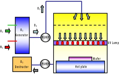
2.2.1 Experiment Details of Ozone Oxide Growth
4 inch p-type (100) silicon wafers were cleaned by standard RCA processes with HF-last for the removal of the particles and native oxides. Figure 2-1 showed the schematic diagram of UV ozone system. The ozone generator (AnserosPAP-2000) decomposed the oxygen molecular to generate ozone gas by high electrical field. The ozone gas was mixed with UV lamp in chamber. By changing the oxygen flow and ozone generation power, the ozone concentration in the chamber could be adjusted. Ozone oxide was grown on Si wafer in the chamber at room temperature. The
relationship between the ozone concentration in the DI water and thickness change of ozone oxide was under investigation. N&K was utilized to measure the ozone oxide thickness.
2.2.2 Different Post Deposition Anneal Characteristics of HfAlOxNy MOS
Devices with Ozone Surface Treatments
Field oxide 5000Å isolated MOS capacitors were fabricated on 4 inch p-type (100) silicon wafers. After forming field oxide isolation, wafers were cleaned by standard RCA processes with HF-last. Prior to high-κ dielectrics deposition, the samples were prepared by Ozone oxide. UV ozone was used to grow an ultra-thin ozone oxide about 9~11Å (measured by N&K). After UV ozone surface treatments, a high temperature 900oC 60seconds was used for densify ozone oxide. HfAlOxNy was
then deposited at room temperature and 7.6E-3 torr by ion sputter system, as shown in Figure 2-2, followed by a different high temperature (as deposition, 500oC, 600oC, 700oC, 800oC,900oC) post deposition annealing (PDA) in the nitrogen ambient for 30 seconds were investigated. Aluminum metal served as the gate electrode was created by a thermal evaporation system. After gate electrodes patterned and backside contact was formed by thermal evaporation. The cross section and the total process flow were shown in Figure. 2-3. Square capacitors of 1×10⁻⁴ cm2 areas with field oxide isolation are used to evaluate the gate oxide integrity. The equivalent oxide thickness (EOT) was extracted by fitting the measured high-frequency (100 kHz) capacitance-voltage (C-V) data from Hewlett-Packard (HP) 4284 LCR meter under accumulation condition. UCLA CVC simulation program was utilized to obtain the accurate flat band voltage (VFB). The C-V hysteresis phenomenon was measured by sweeping the
density-electric field (J-E) and the reliability characteristics of MOS capacitors were measured by semiconductor parameter analyzer HP 4156C.
2.2.3 UV Ozone Treatment and Without UV Ozone Treatment Characteristics of HfAlOxNy MOS Devices
Field oxide 5000Å isolated MOS capacitors were fabricated on 4 inch p-type (100) silicon wafers. After forming field oxide isolation, wafers were cleaned by standard RCA processes with HF-last. Prior to high-κ dielectrics deposition, either the samples were prepared by ozone oxide or without ozone oxide were investigated. UV ozone was used to grow an ultra-thin ozone oxide about 9~11Å (measured by N&K). After UV ozone surface treatments sample with a high temperature 900oC 60seconds was used for density ozone oxide. HfAlOxNy was then deposited at room temperature
and 7.6E-3 torr by ion sputter system. Followed by a high temperature 900oC post deposition annealing (PDA) in the nitrogen ambient for 30 seconds. Aluminum metal served as the gate electrode was created by a thermal evaporation system. After gate electrodes patterned and backside contact was formed by thermal evaporation. The cross section and the total process flow were shown in Figure 2-4. Square capacitors of 1×10⁻⁴ cm2 areas with field oxide isolation are used to evaluate the gate oxide integrity. The equivalent oxide thickness (EOT) was extracted by fitting the measured high-frequency (100 kHz) capacitance-voltage (C-V) data from Hewlett-Packard (HP) 4284 LCR meter under accumulation condition. UCLA CVC simulation program was utilized to obtain the accurate flat band voltage (VFB). The C-V hysteresis
phenomenon was measured by sweeping the gate voltage from accumulation to inversion then back. The tunneling leakage current density-electric field (J-E) and the reliability characteristics of MOS capacitors were measured by semiconductor
parameter analyzer HP 4156C.
2.2.4 NH3 Plasma Treatment on Ozone Surface Treatment Characteristics Of HfAlOxNy MOS Devices
Field oxide 5000Å isolated MOS capacitors were fabricated on 4 inch p-type (100) silicon wafers. After forming field oxide isolation, wafers were cleaned by standard RCA processes with HF-last. Prior to high-κ dielectrics deposition, the samples were prepared by Ozone oxide. UV ozone was used to grow an ultra-thin ozone oxide about 9~11Å (measured by N&K). NH3 plasma treatment (30, 60 90 120 seconds) is prepared of the UV ozone oxide surface. After that a high temperature 900oC 60seconds was used for repair damage at plasma treatment. HfAlOxNy was
then deposited at room temperature and 7.6E-3 torr by ion sputter system. Followed by a high temperature 900oC post deposition annealing (PDA) in the nitrogen ambient for 30 seconds. Aluminum metal served as the gate electrode was created by a thermal evaporation system. After gate electrodes patterned and backside contact was formed by thermal evaporation. The cross section and the total process flow were shown in Figure 2-5. Square capacitors of 1×10⁻⁴ cm2 areas with field oxide isolation are used to evaluate the gate oxide integrity. The equivalent oxide thickness (EOT) was extracted by fitting the measured high-frequency (100 kHz) capacitance-voltage (C-V) data from Hewlett-Packard (HP) 4284 LCR meter under accumulation condition. UCLA CVC simulation program was utilized to obtain the accurate flat band voltage (VFB). The C-V hysteresis phenomenon was measured by sweeping the gate voltage
from accumulation to inversion then back. The tunneling leakage current density-electric field (J-E) and the reliability characteristics of MOS capacitors were measured by semiconductor parameter analyzer HP 4156C.
2.3 Results and Discussions
2.3.1 Basic Property Investigation of the Ozone Oxide
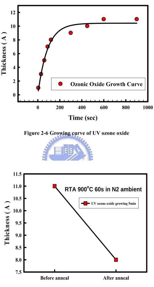
The growth curves of UV ozone oxide as a function of time to grow up shown in Figure 2-6. A saturated oxidation was observed in the growth curves and the resultant self-limiting property could improve the thickness uniformity.
Figure 2-7 shown UV ozone oxide growing 5min with annealing 900oC 60sec in the nitrogen ambient and without. We can observe thinner oxide thickness after a high temperature (RTA 900oC 60sec) because oxide become more densify. We can control the interface layer smaller than 10 Å and decrease EOT.
2.3.2 Different Post Deposition Anneal Characteristics of HfAlOxNy MOS
Devices with Ozone Surface Treatments Effect
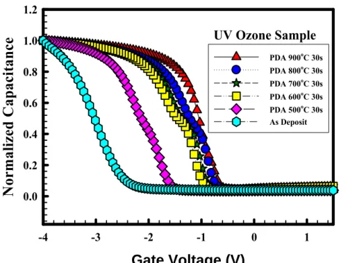
Figure 2-8, Figure 2-9 showed the normalized capacitance-voltage (C-V) characteristics and Vfb Weibull distribution of HfAlOxNy stacked gate dielectrics with
various post deposition anneal on UV ozone treatment samples. Post deposition annealing could reduce the interface trap density exhibited by more sharp C-V characteristics. The C-V curve of Ozone-treated PDA 900oC capacitors was kink free and exhibited good interface properties. From Vfb Weibull distribution, |Vfb|
decreasing depends on PDA temperature increasing. Speculation on inter face state decreasing with PDA temperature increasing.
samples was compared in Figure 2-10. The hysteresis voltage was defined as the flat band voltage difference between the forward and backward swept C-V curves, which might be contributed from the trapped charges within high-κ bulk or interface. The samples without PDA treatment revealed large hysteresis. C-V hysteresis decreasing depends on PDA temperature increasing. Indicate Ozone-treated PDA 900oC sample exhibited almost hysteresis-free characteristics.
Figure 2-11 showed the EOT Weibull distribution of HfAlOxNy stacked gate
dielectrics with various PDA temperatures on UV ozone treatment samples. We can observe that, PDA(500oC~900oC) treatment sample EOT smaller than without treatment(8~11EOT decrement). Therefore, PDA has to do because PDA can improve the high k quality and decrease EOT.
Leakage current density of HfAlOxNy stacked gate dielectrics with various PDA
temperatures on UV ozone treatment as a function of effective electric field (Eeff):
Eeff = ( Vg –Vfb ) / EOT
for samples showed in Figure 2-12. Figure 2-13 showed the Leakage current density at Vfb-1 distribution. From Figure 2-12 and Figure 2-13, indicate 900oC PDA
treatment could lower the leakage current density at Vfb-1 at least 1~2 order. From
leakage density current revealed that a suitable PDA temperature can further improve the dielectric properties.
Synthesized above mentioned in Figure 2-14, PDA treatment could reduced current density at least 1~ 2 orders of magnitude with smaller than 8~11Å EOT decrement.
The time-zero dielectric breakdown (TZDB) reliability investigation were shown in Figs. 3-15. PDA can promote the reliability. Sample without PDA treatment
was supposed to have poor dielectric quality, which will degrade the dielectric reliability. After PDA treatments, the high k dielectric quality was improved, and the reliability therefore became superior.
2.3.3 Comparison of UV Ozone Treatment and Without UV Ozone Treatment Characteristics of HfAlOxNy MOS Devices
Figure 2-16, Figure 2-17 showed the normalized capacitance-voltage (C-V) characteristics and Vfb Weibull distribution of HfAlOxNy gate dielectric PDA 900oC
with ozone surface treatment and without treatment.
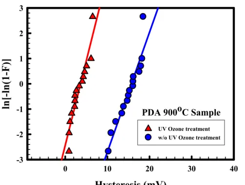
The hysteresis of UV ozone treatment samples and without were compared in Figure 2-18. The hysteresis voltage was defined as the flat band voltage difference between the forward and backward swept C-V curves, which might be contributed from the trapped charges within high-κ bulk or interface. Fortunately, ozone surface treatment resulted in excellent hysteresis behavior.
Figure 2-19 showed the EOT Weibull distribution of HfAlOxNy stacked gate
dielectrics with PDA 900oC on UV ozone treatment samples and without zone treatment. We can observe that, ozone treatment sample EOT smaller than without treatment (1~2Å EOT decrement). Maybe ozone treatment prevent interfacial to grow, therefore ozone treatment sample has smaller EOT.
Leakage current density of HfAlOxNy stacked gate dielectrics with PDA 900oC
on UV ozone treatment samples and without zone treatment were compared. Various surface treatments as a function of effective electric field (Eeff):
for samples showed in Figure 2-20. Figure 2-21 showed the Leakage current density @ Vfb-1 distribution. From Figure 2-20 and Figure 2-21, indicate ozone treatment
could lower the leakage current density at Vfb-1 at least 2.5 times. From leakage
density current revealed that ozone surface treatment can further improve the dielectric properties.
The time-zero dielectric breakdown (TZDB) reliability investigation were shown in Figure 2-22. Ozone treatment can promote the reliability. Sample without surface treatment was supposed to have poor interface between HfAlOxNy and Silicon
substructure which will degrade the dielectric reliability. After ozone surface treatment, the high k dielectric quality was improved, and the reliability therefore became superior.
2.3.4 Comparison of Different NH3 Plasma Treatment on Ozone Surface Characteristics Of HfAlOxNy MOS Devices
Figure 2-23, Figure 2-24 showed the normalized capacitance-voltage (C-V) characteristics and Vfb Weibull distribution of HfAlOxNy gate dielectric PDA 900oC
prior to ozone surface treatment follow various NH3 plasma treatment’s times (30s,
60s, 90s, 120s). From the Vfb weibull and C-V curve we can observer negative Vfb
shift depend on NH3 plasma treatment’s times increase. Indicated NH3 plasma
treatment has positive charges accumulation at interface. Apparent C-V deterioration was observed in NH3 plasma treatment sample due to the excess nitrogen
concentration compels more Si bonding constraints at the interface. Indicate nitrogen at interface bring positive charges. The C-V curve of without NH3 plasma treatment capacitors was kink free and exhibited good interface properties.
The hysteresis of various NH3 plasma treatment’s times on prior UV ozone
treatment samples were compared in Figure 2-25. The hysteresis voltage was defined as the flat band voltage difference between the forward and backward swept C-V curves, which might be contributed from the trapped charges within high-κ bulk or interface. Apparent hysteresis Weibull distribution was observed NH3 plasma
treatment samples exhibited larger hysteresis depend on plasma treatment’s time increasing. Perhaps due to excess nitrogen concentration compels more Si bonding constraints at interface.
Figure 2-26 showed the EOT Weibull distribution of HfAlOxNy gate dielectric
PDA 900oC prior to ozone surface treatment follow various NH3 plasma treatment’s
times. We can observe that, EOT decreasing with NH3 plasma treatment’s time
increasing. Maybe, the increasing of interface layer’s εr is caused by the mixing
nitrogen. Therefore bring about the EOT decrement.
Leakage current density of HfAlOxNy gate dielectric PDA 900oC prior to ozone
surface treatment follow various NH3 plasma treatment’s times were compared.
Various plasma treatment’s time as a function of effective electric field (Eeff):
Eeff = ( Vg –Vfb ) / EOT
for samples showed in Figure 2-27. Figure 2-28 showed the Leakage current density @ Vfb-1 distribution. From Figure 2-27 and Figure 2-28, indicate NH3 plasma
treatment could higher the leakage current density at Vfb-1. From leakage density
current revealed that NH3 plasma treatment maybe damaged the dielectric properties.
The time-zero dielectric breakdown (TZDB) reliability investigation were shown in Figure 2-29. NH3 plasma treatment has poor reliability. NH3 plasma
Silicon substructure which will degrade the dielectric reliability. Maybe excess nitrogen concentration compels more Si bonding constraints at interface or plasma damage the interface.
2.4 Summary
In this chapter, the basic properties of the ozone oxide were studied first. A saturated oxidation was observed in the growth curves and the resultant self-limiting property could improve the thickness uniformity. UV ozone oxide after rapid thermal oxidation become more densify and we can control thickness less 10 Å avoid growing thick interface layer.
Then different post deposition anneal is studied on HfAlOxNy gate dielectric
prior UV ozone treatment. PDA can effectively improve gate dielectric quality. Therefore, post deposition anneal must to do but a suitable anneal temperature is very important on electrical characteristics. In this chapter, we find a suitable anneal temperature to improve electrical characteristics. From the hysteresis , leakage density and time zero to breakdown determine the post deposition anneal at 900 oC and that has excellent electrical characteristics.
We compared with UV ozone treatment and without on electrical characteristics. We observe that, lower EOT and leakage density by UV ozone treatment. Therefore, UV ozone can improve the interface quality. At other electrical characteristic such hystersis also were improved.
HfAlOxNy gate dielectric deposition were investigated. Significantly large fixed
charges and hysteresis of NH3 nitridation would degrade device performance. Form
other electrical characteristics view, though EOT decreasing with the NH3 treatment‘s time increasing but that improvement on electrical characteristic is little. Leakage current density raises with the time of NH3 plasma treatment increasing. Indicate NH3
plasma treatment could higher the leakage current density. From leakage density current revealed that NH3 plasma treatment maybe damaged the dielectric properties.
Time zero to breakdown also shows the bad electrical characteristic on NH3 plasma
O2 N2 O3 Generator O3 Destructor UV Lamp PUMP O3 Wafer O3 Hot plate PUMP
Figure 2-1 UV ozone system schematic diagram
Destructor PUMP N2 O2 Ar Plasma Plasma Al Target Hf Target -V1 -V2 Wafer
RCA Clean with HF-last
UV Ozone Oxide
4 inch p-type (100) Si wafer with FOX (Field Oxide) isolation
Growth of Interface Layer
UV Ozone Oxide Densify RTA 900oC 60s
High_k Deposition Ion sputter is used
Post Deposition Annealing
w/o and RTA 900, 800, 700, 600 oC 30sec in the nitrogen ambient
Metallization & Patterning Al gate & backside contact formation by Thermal Evaporation System
Si FOX Al Al Backside Contact FOX UV Ozone Oxide High K dielectric
RCA Clean with HF-last
Surface Treatment
4 inch p-type (100) Si wafer with FOX (Field Oxide) isolation
(a) UV Ozone treatment (b) Without treatment
Ion sputter is used
Post Deposition Annealing RTA 900oC 30sec in the nitrogen
ambient
Metallization & Patterning Al gate & backside contact formation
by Thermal Evaporation System
High_k Deposition Si FOX Al Al Backside Contact FOX Surface treatment High K dielectric
RCA Clean with HF-last
UV Ozone Oxide
4 inch p-type (100) Si wafer with FOX (Field Oxide) isolation
Growth of Interface Layer
NH3 Plasma Treatment
Si
FOX Al FOX
Al Backside Contact
UV Ozone Oxide+NH3 Plasma
High K dielectric
NH3 Treatment w/o,30,60,90,120s
Repair Plasma Damage RTA 900oC 60s
Post Deposition Annealing RTA 900oC 30sec in the nitrogen
ambient
High_k Deposition
Al gate & backside contact formation by Thermal Evaporation System Ion sputter is used
Metallization & Patterning
Time (sec)
0 200 400 600 800 1000Th
ic
kn
es
s (
A )
0 2 4 6 8 10 12Ozonic Oxide Growth Curve
RTA 900oC 60s in N2 ambient
Before anneal After anneal
Th
ic
k
n
es
s (
A
)
7.5 8.0 8.5 9.0 9.5 10.0 10.5 11.0 11.5UV ozone oxide growing 5min Figure 2-6 Growing curve of UV ozone oxide
Figure 2-7 UV ozone oxide growing 5min with annealing 900oC 60sec in the nitrogen ambient and without
UV Ozone Sample
Gate Voltage (V)
-4 -3 -2 -1 0 1N
orm
al
iz
ed C
apacit
ance
0.0 0.2 0.4 0.6 0.8 1.0 1.2 PDA 900oC 30s PDA 800oC 30s PDA 700oC 30s PDA 600oC 30s PDA 500oC 30s As DepositFigure 2-8 Normalized capacitance-voltage (C-V) characteristics of HfAlOxNy stacked gate
UV Ozone Sample
Flat Band Voltage (V)
-3 -2 -1 0 1
ln
[-ln(1-F
)]
-4 -3 -2 -1 0 1 2 3 PDA 900oC 30s PDA 800oC 30s PDA 700oC 30s PDA 600oC 30s PDA 500oC 30s As Depositdielectrics with various post deposition anneal on UV ozone treatment samples.
Figure 2-9 Vfb Weibull distribution of HfAlOxNy stacked gate dielectrics with various post
UV Ozone Sample
Hysteresis (mV)
1 10 100 1000 10000 100000ln[-ln(1-F
)]
-4 -3 -2 -1 0 1 2 3 PDA 900oC 30s PDA 800oC 30s PDA 700oC 30s PDA 600oC 30s PDA 500oC 30s As DepositFigure 2-10 The hysteresis of various post deposition anneal on UV ozone treatment UV Ozone Sample
EOT(A)
35 40 45 50 55ln
[-ln(1-F
)]
-3 -2 -1 0 1 2 3 4 PDA 900oC 30s PDA 800oC 30s PDA 700oC 30s PDA 600oC 30s PDA 500oC 30s As Deposit PDA treatment Without PDA treatmentFigure 2-11 EOT Weibull distribution of HfAlOxNy stacked gate dielectrics with various PDA temperatures on UV ozone treatment samples.
UV Ozone Sample
Effect Field (MV/cm)
-40 -30 -20 -10 0J (
A
/cm
2 )
10-10 10-9 10-8 10-7 10-6 10-5 10-4 10-3 10-2 10-1 100 101 102 103 104 PDA 900oC 30s PDA 800oC 30s PDA 700oC 30s PDA 600oC 30s PDA 500oC 30s As Deposit UV Ozone SampleLeakage Current Density @ Vfb-1 (A/cm
2)
10-8 10-7 10-6 10-5 10-4
ln[-ln(1-F)]
-3 -2 -1 0 1 2 3 PDA 900oC 30s PDA 800oC 30s PDA 700oC 30s PDA 600oC 30s PDA 500oC 30s As DepositFigure 2-12 Leakage current density of HfAlOxNy stacked gate dielectrics with various PDA temperatures on UV ozone treatment
Figure2-13 Leakage current density at Vfb-1 distribution of
HfAlOxNy stacked gate dielectrics with various PDA temperatures on UV ozone treatment samples.
UV Ozone Sample
PDA Temperature
900 800 700 600 500 w/o PDAEO
T(
A
)
32 34 36 38 40 42 44 46 48 50L
eak
ag
e C
u
rren
t D
en
si
ty
@
V
fb
-1
10-10 10-9 10-8 10-7 10-6 10-5 10-4 10-3Figure 2-14 Assembled the EOT and leakage current density at Vfb-1
of HfAlOxNy stacked gate dielectrics with various PDA temperatures on UV ozone treatment samples.
UV Ozone Sample
Breakdown Field(MV/cm)
5 10 15 20 25 30ln[-ln(1-F
)]
-3 -2 -1 0 1 2 3 PDA 900oC 30s PDA 800oC 30s PDA 700oC 30s PDA 600oC 30s PDA 500oC 30s As DepositFigure 2-15 TZBD of HfAlOxNy stacked gate dielectrics with various PDA temperatures on UV ozone treatment samples.
PDA 900oC Sample
Gate Voltage (V)
-5 -4 -3 -2 -1 0 1 2N
orm
al
iz
ed
C
ap
aci
tan
ce
0.0 0.2 0.4 0.6 0.8 1.0 1.2 UV Ozone Treatment w/o UV Ozone TreatmentPDA 900oC Sample
Flat Band Voltage (V)
-1.6 -1.4 -1.2 -1.0 -0.8 -0.6 -0.4 -0.2 0.0
ln
[-ln
(1-F
)]
-3 -2 -1 0 1 2 3 UV Ozone treatment w/o UV Ozone treatmentFigure 2-16 Normalized capacitance-voltage (C-V) characteristics of HfAlOxNygate dielectric PDA 900oC with ozone surface
treatment and without treatment.
Figure 2-17 Vfb Weibull distribution of HfAlOxNygate dielectric PDA
PDA 900oC Sample
Hysteresis (mV)
0 10 20 30 40ln[-ln(1-F
)]
-3 -2 -1 0 1 2 3 UV Ozone treatment w/o UV Ozone treatmentPDA 900oC Sample
EOT(A)
28 30 32 34 36 38 40ln[-ln(1-F
)]
-3 -2 -1 0 1 2 3 UV Ozone treatment w/o UV Ozone treatmentFigure 2-18 The hysteresis of UV ozone treatment samples and without
Figure2-19 EOT Weibull distribution of HfAlOxNy stacked gate dielectrics with PDA 900oC on UV ozone treatment samples and without zone treatment.
PDA 900oC Sample
Effect Field (MV/cm)
-50 -40 -30 -20 -10 0L
eakage C
u
rrent
D
ens
it
y (
A
/c
m
2 )
10-9 10-8 10-7 10-6 10-5 10-4 10-3 10-2 10-1 100 101 102 103 UV Ozone Treatment w/o UV Ozone TreatmentFigure 2-20 Compare with leakage current density of HfAlOxNy stacked gate dielectrics with PDA 900oC on UV ozone treatment samples and without zone treatment.
PDA 900oC Sample
Leakage Current Density @ Vfb-1 (A/cm
2)
10-8 10-7 10-6
ln[-ln(1-F)]
-3 -2 -1 0 1 2 3 UV Ozone treatment w/o UV Ozone treatmentFigure 2-21 Leakage current density @ Vfb-1 distribution of HfAlOxNy
stacked gate dielectrics with PDA 900oC on UV ozone treatment samples and without zone treatment.
PDA 900oC Sample
Breakdown Field(MV/cm)
12 14 16 18 20 22 24ln[-ln(1-F
)]
-3 -2 -1 0 1 2 3 UV Ozone treatment w/o UV Ozone treatmentFigure 2-22 The time-zero dielectric breakdown (TZDB) of HfAlOxNy stacked gate dielectrics with PDA 900oC on UV ozone treatment samples and without zone treatment.
Ozone Treatment PDA 900oC Sample
Gate Voltage (V)
-5 -4 -3 -2 -1 0 1 2N
orm
al
iz
ed
C
ap
aci
tan
ce
0.0 0.2 0.4 0.6 0.8 1.0 1.2 w/o NH3 Treatment NH3 Treatment 30 sec NH3 Treatment 60 sec NH3 Treatment 90 sec NH3 Treatment 120 secFigure 2-23 Normalized capacitance-voltage (C-V) characteristics of HfAlOxNygate dielectric PDA 900oC prior to ozone
surface treatment follow various NH3 plasma
treatment’s times.
Ozone Treatment PDA 900oC Sample
Flat Band Voltage
-1.6 -1.4 -1.2 -1.0 -0.8 -0.6
ln[-ln(1-F
)]
-4 -3 -2 -1 0 1 2 3 w/o NH3 Treatment NH3 Treatment 30 sec NH3 Treatment 60 sec NH3 Treatment 90 sec NH3 Treatment 120 secFigure 2-24 Vfb Weibull distribution of HfAlOxNygate dielectric
PDA 900oC prior to ozone surface treatment follow various NH3 plasma treatment’s times.
Ozone Treatment PDA 900oC Sample
Hysteresis (mV)
0 10 20 30 40ln[-ln(1-F
)]
-3 -2 -1 0 1 2 3 4 w/o NH3 Treatment NH3 Treatment 30 sec NH3 Treatment 60 sec NH3 Treatment 90 sec NH3 Treatment 120 secFigure 2-25 The hysteresis of of HfAlOxNygate dielectric
PDA 900oC prior to ozone surface treatment follow various NH3 plasma treatment’s times.
Ozone Treatment PDA 900oC Sample
EOT(A)
26 28 30 32 34 36 38 40ln[-ln(1-F
)]
-3 -2 -1 0 1 2 3 w/o NH3 Treatment NH3 Treatment 30 sec NH3 Treatment 60 sec NH3 Treatment 90 sec NH3 Treatment 120 secFigure 2-26 EOT of of HfAlOxNygate dielectric PDA 900oC
prior to ozone surface treatment follow various NH3 plasma treatment’s times.
Ozone Treatment PDA 900oC Sample
Effect Field (MV/cm)
-50 -40 -30 -20 -10 0L
eakage C
urrent
D
ens
it
y (
A
/c
m
2 )
10-9 10-8 10-7 10-6 10-5 10-4 10-3 10-2 10-1 100 101 102 103 w/o NH3 Treatment NH3 Treatment 30 sec NH3 Treatment 60 sec NH3 Treatment 90 sec NH3 Treatment 120 sec Ozone Treatment PDA 900oC SampleLeakage Current Density @ Vfb-1 (A/cm2)
10-8 10-7 10-6 10-5 10-4 ln [-l n (1 -F )] -3 -2 -1 0 1 2 3 w/o NH3 Treatment NH3 Treatment 30 sec NH3 Treatment 60 sec NH3 Treatment 90 sec NH3 Treatment 120 sec
Figure 2-27 Leakage current density of of HfAlOxNygate dielectric
PDA 900oC prior to ozone surface treatment follow various NH3 plasma treatment’s times
Figure 2-28 Leakage current density @ Vfb-1 distribution of of
HfAlOxNygate dielectric PDA 900oC prior to ozone surface
Ozone Treatment PDA 900oC Sample
Breakdown Field(MV/cm)
12 14 16 18 20 22 24 26ln[-ln(1-F
)]
-3 -2 -1 0 1 2 3 w/o NH3 Treatment NH3 Treatment 30 sec NH3 Treatment 60 sec NH3 Treatment 90 sec NH3 Treatment 120 secFigure 2-29 The time-zero dielectric breakdown (TZDB) of HfAlOxNy
gate dielectric PDA 900oC prior to ozone surface treatment follow various NH3 plasma treatment’s times
CHAPTER 3
HfAlO
xN
yMOS FET Devices Characteristics
3.1 Introduction
Unlike SiO2 films, high-k films are more susceptible to charge trapping. Charge trapping is arguable one of the most important issue in CMOS devices with high k gate dielectrics, because of the large amount of bulk traps present in the high k films [25]-[28]. The existence of bulk trap unavoidably causes many unwanted problems, such as reliability degradation [29], mobility degradation [30]-[34] and threshold voltage instability [35]-[44]. Charge pumping measurement is widely used to estimate interface state density in MOSFET devices. This measurement is very effective because it allows the exclusion of gate leakage contribution to the calculated interface state density presented in thin gate oxides.
Recently, reliability is an important issue in scaled MOSFET. During positive bias stress defects can be generated in the devices, which in turn cause threshold voltage shifts and device characteristics degradation. The device parameter variation can lead to circuit failures, both for analog and digital application.
In this work, we used optimum condition (UV ozone treatment and PDA 900oC 30 seconds after high k film deposit) on chapter two to fabricate the nMOSFETs. A control sample (without treatment and PDA900oC 30seconds after high k film deposit) was fabricate at the same time. In this chapter we compare to this two samples on electrical characteristic. We found that UV ozone treatment effectively improve the electrical characteristics, such interface state density, electric mobility, transconductance and ect. We investigate energy distribution of the interface traps in a
relatively large part of the forbidden energy gap on both sides of midgap by measuring the charge pumping currents (Icp) with variable fall and rise times.
3.2
Experiment Details
In this thesis, field oxide was used for device isolation. MOS transistors was fabricated on 4-inch p-type Si with ( 1 0 0 ) orientation. After removing the native oxide, RCA clean was performed with HF-dip last, and immediately split into two groups. One is UV ozone treatment and the other is without UV ozone treatment. (UV ozone was used to grow an ultra-thin ozone oxide about 9~11Å (measured by N&K). After UV ozone surface treatments sample with a high temperature 900oC 60seconds
was used for density ozone oxide. On above step we called UV ozone treatment.) After surface treatment HfAlOxNy was deposited at room temperature and 7.6E-3 torr
by ion sputter system. Followed by a high temperature 900oC post deposition
annealing (PDA) in the nitrogen ambient for 30 seconds in order to improve the film quality. A 200nm undoped polycrystalline silicon (poly-Si) layer was directly deposited by low pressure chemical vapor deposition (LPCVD) on top of HfAlOxNy
films. After the gate electrode was patterned by lithography and etching processing. Then implant As 20 KeV dose 5E15 #/cm2 after that activation was done at 950 oC by
SiO2 passivation was done by PECVD. Define the contact hole by the lithography and
etching passivation SiO2 and high k layer in order to silicon contact whit metal. Al
was deposited by thermal evaporation system. Metal pad is defined by lithography and etching. Backside contact was formed by thermal evaporation. Figure 3-1 shown The cross section and the key process flow.
Current-voltage (I-V) and capacitance-voltage(C-V) characteristics were evaluated by an HP4156A precision semiconductor parameter analyzer and HP4284 LCR meter, respectively. The equivalent oxide thickness (EOT) of the gate dielectric was obtained from high frequency (100 KHz) capacitance-voltage (C-V) curve at strong inversion without considering quantum effect.
The hysteresis phenomenon was measured by sweeping the gate voltage from accumulation to inversion then back. Determine that by measurement Vt shift
difference between forward and reverse.
In this thesis, the interface trap density (Nit) was analyzed using the charging
pumping technique [3-18]. Square-wave waveforms (f = 1MHz) were applied to the gate by 811110A plus generator, and the base voltage was varied from accumulation to inversion, while keeping the pulse amplitude at 1.5V. Figure 3-2 shows the configuration of measurement setup used in our charge pumping experiment. A MOSFET with area AG gives the charge pumping current as:
cp G it
I =qA fN (3-1)
Interface trap density could be extracted from the above equation.
The total trap density increase, ΔNtot which includes the increade of interface
trap density and bulk trap density, was calculated from ΔVth bv assuming that the
charge was trapped at the interface between the dielectric and substrate.
th tot G C V N qA = (3-2) However, By measuring the charge pumping currents (Icp) with variable fall and
rise times, one can obtain the energy distribution of the interface traps in a relatively large part of the forbidden energy gap on both sides of midgap [3-19][3-20].
Therefore, interface traps act is donor-like or acceptor-like which depend on their relative state to the band gap. Relative position depends on its fermi level and an interface trap will be occupied by an electron or empty. Meanwhile, we listed some useful equations for analyzing whether acceptor like interface states or donor like interface states. | | 2 ln ln | | cp fb t it G r f th i n p a I V V qD A kT t t V n f V σ σ ⎧ ⎛ − ⎞⎫ ⎪ ⎪ = ⎨ + ⎜ ⎬ ⎪ ⎝ ⎠⎪ ⎩ ⎟ (3-3) ⎭ ( , ) , | | ln( ) | | Ei Ef inv fb t kT em e i th i n f a V V E E kT V n t e V σ − − − = − + (3-4) ( , , | | ln( ) | | Ei Ef acc fb t kT em h i th i p r a V V E E kT V n t e V σ − − − ) − = + + (3-5) 2 ( ) f cp it G f t dI N E qA Tf dt = − (tr constant) (3-6)