Numerical analysis on the effect of electron blocking layer in 365-nm
ultraviolet light-emitting diodes
Fang-Ming Chen
1,*, Jih-Yuan Chang
2, Yen-Kuang Kuo
3, Bing-Cheng Lin
4, and Hao-Chung Kuo
41
Institute of Photonics, National Changhua University of Education, Changhua 500, Taiwan
2Kuang-Ming Junior High School, Taichung 400, Taiwan
3
Department of Physics, National Changhua University of Education, Changhua 500, Taiwan
4Department of Photonics and Institute of Electro-Optical Engineering, National Chiao Tung
University, Hsinchu 30010, Taiwan
*Tel: +886-4/7232105 Ext. 3365, Fax: +886-4/721-1153, E-mail: [email protected]
ABSTRACT
For 365-nm ultraviolet light-emitting diodes (UV LEDs), an electron blocking layer (EBL) is usually utilized to mitigate electron overflow. However, using EBL might obstruct holes from injecting into the active region. Moreover, the large polarization field in conventional EBL might also pull down the effective barrier height for electrons, and thus the electrons could easily overflow to the p-side region. To solve the above drawbacks, in this study, the Al content and p-doping concentration of the EBL in typical 365-nm UV LEDs are investigated systematically. Specifically, designs of AlGaN/GaN superlattice EBL and Al-content-graded EBL are explored in detail.
Keywords: ultraviolet light-emitting diodes, electron blocking layer, polarization
1. INTRODUCTION
The 365-nm ultraviolet light-emitting diodes (UV LEDs) are of special interest for curing light source, biochemistry, sensing, and data storage applications1. To enhance the device performance, various approaches including crystal quality
enhancement2, increasing p-doping efficiency3, improving light extraction efficiency4, decreasing self-heating5, carrier
confinement improvement6, and usage of non-polar or semi-polar substrate7 have been reported. Among the numerous
suggestions, the weak carrier confinement should be a significant issue due to the shallow well and polarization field in both the active region and electron blocking layer (EBL). The employment of AlGaN material as an EBL is usually believed to be necessary for blocking the electrons from overflowing to the p-side region. When the Al-content in AlGaN EBL is increased, the energy bandgap of EBL increases. However, the polarization mismatch and the relevant polarization field, which create serious polarization-induced band-bending and thus lower the electron-blocking capability, increase as well. Moreover, the wide-bandgap EBL also creates a potential barrier in the valance band and thus obstructs the holes from p-side into the active region. The Al-content in EBL therefore needs to be carefully considered/adjusted in order to achieve the superior performance. In addition, the p-type doping concentrations in EBL which corresponds to the hole injection efficiency should be another issue to obtain the higher-power UV LEDs. Several suggestions about the design of EBL in UV LEDs have been reported, such as adopting the AlGaInN polarization-matched8 or AlGaInN polarization-reversed9 EBL, grading Al-content AlGaN EBL10, and
AlGaN/GaN-superlattice EBL11. Note that although there are advantages for the use of quaternary AlGaInN EBL, there
still exist limitations till now, such as the degradation of crystalline quality or even failure to obtain the AlGaInN crystal film. In this study, with the purpose of effectively reducing the electron leakage and enhancing the hole injection efficiency, the Al-content and Mg-doping concentrations of the EBL in 365-nm UV LED are investigated systematically. Specifically, since there were no comparisons between the employment of grading Al-content AlGaN EBL and AlGaN/GaN-superlattice EBL have been made in the literature, designs of superlattice as EBL and Al-content-graded EBL are explored in detail. All the systematical investigations and specific designs for the EBL of 365-nm UV LEDs are
simulated with the APSYS simulation program so as to improve the efficiency of hole injection without losing the blocking capability of electron overflow and consequently optimize the output performance of UV LEDs.
2. PHYSICAL MODEL AND PARAMETERS
For the 365-nm UV LED under study, the original GaN-based UV LED structure as a reference, which has peak emission wavelength of approximately 365-nm around 60 mA, was grown on c-plane sapphire substrate by metal organic chemical vapor deposition (MOCVD). This LED structure is composed of a 2.5-μm-thick n-Al0.039Ga0.961N layer
(Si-doping: 5 × 1018 cm−3), ten pairs of In
0.04Ga0.96N/Al0.16Ga0.82In0.02N MQWs with 2.5-nm-thick wells and 10-nm-thick
barriers, 17-nm-thick p-Al0.3Ga0.7N EBL (Mg-doping: 1 × 1019 cm−3), 13-nm-thick p-Al0.1Ga0.9N (Mg-doping: 1 × 10¹⁹
cm−3), and 55-nm-thick p-GaN contact layer (Mg-doping: 5 × 1019 cm−3). The mesa size was 1000 × 1000 μm2. In the
simulation, the light extraction efficiency and background loss are assumed to be 40% and 20 cm−1. The Shockley-Read-Hall (SRH), radiative recombination, and Auger recombination coefficients are set to 5 × 10⁷ s–1, 2 ×
10−11 cm3 s–1, and 9.5 × 10⁻³¹ cm6 s–1, respectively. The polarization-induced surface charges at the interfaces are
calculated by the methods developed by Fiorentini et al.12 Considering the screening caused by defects, the surface
charge densities are assumed to be 55% of the calculated values so that the output performance of this UV LED obtained from simulation can be best matched to the experiment data. The band-offset ratio is assumed to be 0.65/0.35 for 365-nm UV LEDs. The energy bandgaps of unstrained nitride-based materials are calculated by the formula proposed by Vurgaftman et al.13 The unstrained bandgap energies of the AlGaInN quaternary alloy can be expressed as
𝐸𝑔(𝐴𝑙𝑥𝐺𝑎𝑧𝐼𝑛𝑦𝑁) =𝑥∙𝑦∙𝑇𝐴𝑙𝐼𝑛𝑁(𝑢)+𝑦∙𝑧∙𝑇𝑥∙𝑦+𝑦∙𝑧+𝑥∙𝑧𝐼𝑛𝐺𝑎𝑁(𝑣)+𝑥∙𝑧∙𝑇𝐴𝑙𝐺𝑎𝑁(𝑤) (1)
𝑇𝐴𝑙𝐼𝑛𝑁(𝑢) = 𝑢 ∙ 𝐸𝑔,𝐼𝑛𝑁+ (1 − 𝑢) ∙ 𝐸𝑔,𝐴𝑙𝑁+ 𝐵𝐴𝑙𝐼𝑛𝑁∙ 𝑢 ∙ (1 − 𝑢) (2)
𝑇𝐼𝑛𝐺𝑎𝑁(𝑣) = 𝑣 ∙ 𝐸𝑔,𝐺𝑎𝑁+ (1 − 𝑣) ∙ 𝐸𝑔,𝐼𝑛𝑁+ 𝐵𝐼𝑛𝐺𝑎𝑁∙ 𝑣 ∙ (1 − 𝑣) (3)
𝑇𝐴𝑙𝐺𝑎𝑁(𝑤) = 𝑤 ∙ 𝐸𝑔,𝐺𝑎𝑁+ (1 − 𝑤) ∙ 𝐸𝑔,𝐴𝑙𝑁+ 𝐵𝐴𝑙𝐺𝑎𝑁∙ 𝑤 ∙ (1 − 𝑤) (4)
𝑢 =1−𝑥+𝑦2 , 𝑣 =1−𝑦+𝑧2 , 𝑤 =1−𝑥+𝑧2 (5)
Where x, y, and z = 1–x–y represent the compositions of aluminum (Al), indium (In), and gallium (Ga) in the AlGaInN material system. 𝐵𝐴𝑙𝐼𝑛𝑁, 𝐵𝐼𝑛𝐺𝑎𝑁, and 𝐵𝐴𝑙𝐺𝑎𝑁 are the bandgap bowing parameters of AlInN, InGaN, and AlGaN, that are assumed to be 3.6 eV, 2.0 eV, and 0.24 eV, respectively. 𝐸𝑔,𝐼𝑛𝑁, 𝐸𝑔,𝐴𝑙𝑁, and 𝐸𝑔,𝐺𝑎𝑁 are the bandgap energies of InN, AlN, and GaN, which have values of 0.641 eV, 5.965 eV, and 3.417 eV at 300K, respectively. The Caughey– Thomas approximation is employed for the low-field mobility as a function of carrier density14 𝜇0(𝑁) = 𝜇𝑚𝑖𝑛+1+(𝑁 𝑁𝜇𝑚𝑖𝑛−𝜇𝑚𝑎𝑥 𝑟𝑒𝑓 ⁄ )𝛼 (6)
Moreover, the high-field electron mobility is expressed by the formula15 𝜇𝑒(𝐹) = 𝜇𝑒𝑜(𝑁)−𝜇𝑒,𝑠𝑎𝑡(𝐹𝛽1−1/𝐹0𝛽1) 1+(𝐹/𝐹0)𝛽1+𝑎(𝐹 𝐹⁄ )0 𝛽2 (7)
and the standard Caughey–Thomas formula is used to calculate the high-field hole mobility14 𝜇ℎ(𝐹) =1+𝜇𝜇ℎ𝑜(𝑁)𝐹 ℎ𝑜(𝑁)𝐹 𝜇⁄ ℎ,𝑠𝑎𝑡 (8)
For the electrons of AlGaN alloys, the values of 𝜇𝑚𝑎𝑥, 𝜇𝑚𝑖𝑛, 𝑁𝑟𝑒𝑓, and 𝛼 are 306 cm2/Vs, 132 cm2/Vs, 1.0 × 10¹⁷
cm−3, and 0.29, respectively. The low-field hole mobility are assumed to be 10 cm2/V
s. The parameters, 𝜇𝑒,𝑠𝑎𝑡, 𝜇ℎ,𝑠𝑎𝑡,
kV/cm, 5.3, and 1.0, respectively. The doped carrier densities in the simulation represent actual densities of free carriers. Other material parameters used in the simulation can be found in Ref [16].
3. SIMULATION RESULTS
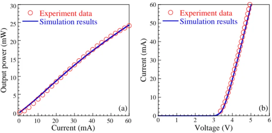
Figure 1 plots the experimental (open dots) and simulated (solid curves) (a) light output power versus current (L – I) and (b) current as a function of voltage (I – V) characteristics of the original 365-nm UV LED. The output power of this UV LED is 24.1 mW at 60 mA with operation voltage around 4.9 V. According to both L – I andI – V curves, it is observed that the simulation results are in good agreement with experimental data.
Fig. 1. Experimental (open dots) and simulated (solid curves) (a) L – I and (b) I – V characteristics of the original 365-UV LED.
3.1 Al-content in AlGaN EBL
In this section, the optical and electrical performances of 365-nm UV LED with various Al-content in AlGaN EBL are systematically studied. The light output power at 60 mA as a function of Al-content of EBL and the I – V characteristics of the structures with Al0.1Ga0.9N, Al0.2Ga0.8N, and Al0.3Ga0.7N EBLs are shown in Figs. 2(a) and 2(b), respectively. In
Fig. 2(a), it is found that the structure with Al0.2Ga0.8N EBL has the best light output power at 60 mA. Besides, the
operation voltage of the LED is reduced when the Al-content of EBL is decreased, as shown in Fig. 2(b). Note that there exists an obvious increment between Al0.2Ga0.8N and Al0.3Ga0.7N structures.
Fig. 2. Simulated (a) light output power at 60 mA as a function of Al-content of EBL and (b) I – V characteristics of the structures with Al0.1Ga0.9N, Al0.2Ga0.8N, and Al0.3Ga0.7N EBLs. Note that the LED with Al0.3Ga0.7N EBL is the original LED structure.
0 5 10 15 20 25 30 0 10 20 30 40 50 60 Experiment data Simulation results Ou tpu t po wer (m W) Current (mA) (a) 0 10 20 30 40 50 60 0 1 2 3 4 5 6 Experiment data Simulation results Cu rren t (m A) Voltage (V) (b) 10 15 20 25 30 10 15 20 25 30 Ou tpu t po w e r (m W) Al-content (%) @ 60 mA (a) 0 10 20 30 40 50 60 2.0 2.5 3.0 3.5 4.0 4.5 5.0 Al0.1Ga0.9N Al0.2Ga0.8N Al0.3Ga0.7N Cu rren t (m A) Voltage (V) (b)
Fig. 3. Energy band diagrams near EBL of the structures with (a) Al0.1Ga0.9N, (b) Al0.2Ga0.8N, and (c) Al0.3Ga0.7N EBL at 60 mA.
Figure 3 shows the energy band diagrams near EBL of the structures with Al0.1Ga0.9N, Al0.2Ga0.8N, and Al0.3Ga0.7N EBL
at 60 mA. In this figure, the effective potential height of EBL for electrons (ΔEc), which is defined as the difference
between quasi-Fermi level and the band edge at conduction band maximum of EBL, is calculated to estimate the blocking capability for electron leakage. It is observed that, since the bandgap energy increases with the increase of Al content, ΔEc of the structure with Al0.2Ga0.8N EBL is much higher than that of the structure with Al0.1Ga0.9N one (427
meV versus 300 meV). However, there exists a trade-off that the polarization mismatch between last barrier and EBL also increases when an EBL with higher Al content is employed. In this case, the polarization fields in last barrier and EBL are higher, and the LED structure thus suffers from more serious band bending and insufficient electron-blocking capability of EBL. In Fig. 3(c), ΔEc of the structure with Al0.3Ga0.7N EBL is 392 meV, which is even smaller than the
Al0.2Ga0.8N structure.
Fig. 4. Distribution of electron concentrations near EBL of the structures with Al0.1Ga0.9N, Al0.2Ga0.8N, and Al0.3Ga0.7N EBL at 60 mA.
Figure 4 shows the distribution of electron concentrations near EBL of the structures with Al0.1Ga0.9N, Al0.2Ga0.8N, and
Al0.3Ga0.7N EBL at 60 mA. Evidently, the amount of electrons that leak out of the active region is markedly reduced
when Al0.2Ga0.8N EBL is employed. The result coincides with the above analyses of energy bandgap and the light output
power should be effectively improved when Al0.3Ga0.7N EBL (original EBL) is replaced by Al0.2Ga0.8N EBL.
2.64 2.65 2.66 2.67 2.68 Distance (m) (b) Ec = 427 meV quasi-Fermi levels Al0.2Ga0.8N @ 60 mA p-side 2.64 2.65 2.66 2.67 2.68 Distance (m) (c) Ec = 392 meV quasi-Fermi levels Al0.3Ga0.7N @ 60 mA p-side -1 0 3 4 5 2.64 2.65 2.66 2.67 2.68 En ergy (eV ) Distance (m) @ 60 mA Al0.1Ga0.9N (a) Ec = 300 meV quasi-Fermi levels p-side 10 12 14 16 18 20 2.64 2.65 2.66 2.67 2.68
Al
0.1Ga
0.9N
Al
0.2Ga
0.8N
Al
0.3Ga
0.7N
Ele
ctro
n co
nc
entr
ati
ons
,
log
(c
m
-3)
Distance (
m)
@ 60 mA
3.2 Al-content and Mg-doping concentration in AlGaN EBL
In this section, the optical and electrical performances of 365-nm UV LEDs with various Al-content and Mg-doping concentrations in AlGaN EBL are systematically studied. The light output power at 60 mA as a function of Al-content of EBL and the I – V characteristics of the structure with Al0.2Ga0.8N EBL when the Mg-doping concentrations are 1 × 10¹⁸
cm−3, 5 × 1018 cm−3, and 1 × 1019 cm−3 respectively are shown in Figs. 5(a) and 5(b). It is obvious that the optical and
electrical properties are promoted, i.e. higher output power and lower operation voltage, when higher Mg-doping concentration is adopted.
Fig. 5. Simulated (a) light output power at 60 mA as a function of Al-content of EBL and (b) I – V characteristics of the structure with Al0.2Ga0.8N EBL when the Mg-doping concentrations are 1 × 1018 cm−3, 5 × 1018 cm−3, and 1 × 1019 cm−3 respectively.
Fig. 6. Energy band diagrams near EBL of the structures with Al0.2Ga0.8N EBL and (a) 1 × 1019 cm−3 and (b) 1 × 1018 cm−3 Mg-doping concentration at 60 mA.
Figure 6 shows the energy band diagrams near EBL of the structures with Al0.2Ga0.8N EBL and (a) 1 × 1019 cm−3 and (b)
1 × 1018 cm−3 Mg-doping concentration at 60 mA. When the Al
0.2Ga0.8N EBL is with higher Mg-doping concentration,
ΔEc increases while the effective potential height for holes of EBL (ΔEv) decreases simultaneously. Under the
circumstances, electrons of the active region are with higher confinement and holes in the p-side can inject into the active region more effectively.
0 10 20 30 40 50 60 2.0 2.5 3.0 3.5 4.0 4.5 5.0 Mg = 1x10¹⁸ (cm-3) Mg = 5x10¹⁸ (cm-3) Mg = 1x10¹⁹ (cm-3) Cu rren t (m A) Voltage (V) Al0.2Ga0.8N EBL 5 10 15 20 25 30 10 15 20 25 30 Mg = 1x10¹⁸ (cm-3) Mg = 5x10¹⁸ (cm-3) Mg = 1x10¹⁹ (cm-3) Ou tpu t po w e r (m W) Al content (%) @ 60 mA 2.64 2.65 2.66 2.67 2.68 Distance (m) (b) Ec = 320 meV quasi-Fermi levels Mg-doped = 1x10¹⁸ (cm-3) @ 60 mA Ev = 338 meV -1 0 3 4 5 2.64 2.65 2.66 2.67 2.68 En ergy (eV ) Distance (m) (a) Ec = 427 meV quasi-Fermi levels Mg-doped = 1x10¹⁹ (cm-3) @ 60 mA Ev = 292 meV
Fig. 7. Distribution of (a) electron concentrations and (b) hole concentrations near EBL of the UV LED structures with Al0.2Ga0.8N EBL and 1 × 1018 cm−3, 5 × 1018 cm−3, and 1 × 1019 cm−3 Mg-doping concentrations.
The distribution of electron concentrations and hole concentrations near EBL of the UV LED structures with Al0.2Ga0.8N
EBL and 1 × 1018 cm−3, 5 × 1018 cm−3, and 1 × 1019 cm−3 Mg-doping concentrations are shown in Figure 7. It is found the
amount of electrons that leak out of the active region is markedly increased and the holes inject into the active region is decreased when the Mg-doping concentration of EBL is reduced. The light output power and the electrical performance are therefore improved.
3.3 Comparison of AlGaN/GaN superlattice EBL and Al-content-graded EBL
In this section, the UV LED structures with AlGaN/GaN superlattice EBL and Al-content-graded EBL are compared numerically. The “original EBL” represents the structure with original Al0.3Ga0.7N EBL (17-nm-thick). In the structure
with “gradual EBL”, the original EBL is replaced by a 30-nm-thick AlGaN EBL in which the Al content is linearly graded from 10% to 20%. As for the structure with “SL EBL”, the original EBL is replaced by seven pairs Al0.2Ga0.8N/Al0.1Ga0.9N (2 nm / 2nm) periodical superlattice layers. Note that, for the latter two structures, the thickness
of p-Al0.1Ga0.9N layer is relevantly reduced in order to keep the total thickness unchanged.
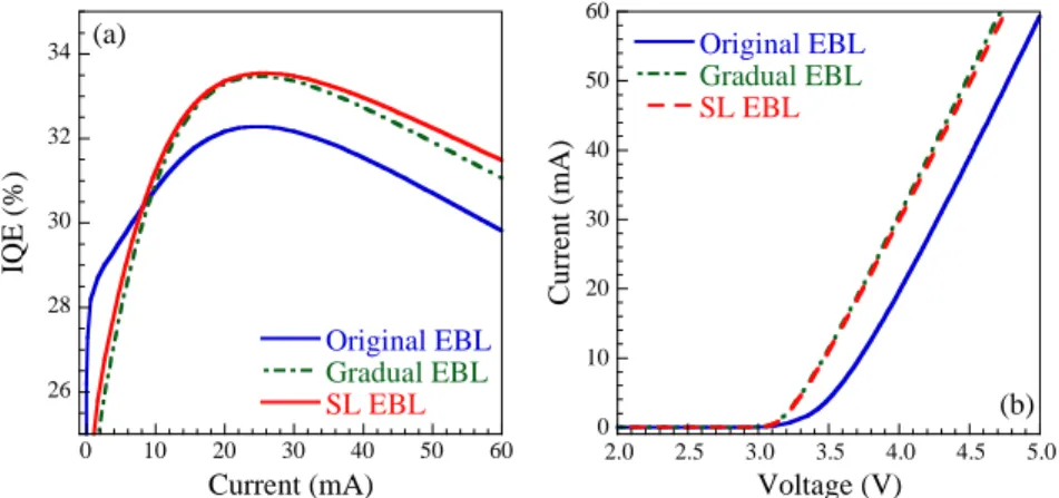
Fig. 8. Simulated (a) IQE curves and (b) I – V characteristics of the 365-nm UV LEDs with original EBL, gradual EBL, and SL EBL.
10 12 14 16 18 20 2.64 2.65 2.66 2.67 2.68 Ho le c oncen trati ons , log (c m -3) Distance (m) @ 60 mA (b) 10 12 14 16 18 20 Mg = 1x10¹⁸ Mg = 5x10¹⁸ Mg = 1x10¹⁹ Ele ctro n co nce ntr ation s, log (c m -3) @ 60 mA (a) 0 10 20 30 40 50 60 2.0 2.5 3.0 3.5 4.0 4.5 5.0 Original EBL Gradual EBL SL EBL Cu rren t (m A) Voltage (V) (b) 26 28 30 32 34 0 10 20 30 40 50 60 Original EBL Gradual EBL SL EBL Current (mA) IQ E ( %) (a)
Figure 8 shows the IQE curves and I – V characteristics of the 365-nm UV LEDs with original EBL, gradual EBL, and SL EBL. In Fig. 8(a), it is found that the IQEs of the structures with gradual EBL and SL EBL are better than that of the original structure with Al0.3Ga0.7N EBL. Furthermore, the turn-on voltages of the two new-proposed structures are
markedly reduced as well, as shown in Fig. 8(b).
Fig. 9. Energy band diagrams near EBL of the structures with (a) original EBL, (b) gradual EBL, and (c) SL EBL at 60 mA.
Figure 9 shows the energy band diagrams near EBL of the structures with original EBL, gradual EBL, and SL EBL at 60 mA. It is interesting that ΔEc of all the three structures are identical (=392 meV), indicating that the capabilities for
electron blocking are similar. While for holes, ΔEv of the structures with original EBL, gradual EBL, and SL EBL at 60
mA are 353 meV, 338 meV, and 322 meV, respectively. The efficiency of hole injection thus plays an important role for the various optical and electrical characteristics of these structures. The simulation results suggest that, among the structures, the one with SL EBL has optimal performance at 60 mA due to its lowest effective potential barrier height for holes.
4. CONCLUSION
In this paper, optimizations of 365-nm UV LEDs with various Al-content and Mg-doping concentrations of EBL are systematical studied. In addition, specific designs on band structure of EBL in 365-nm UV LEDs, including conventional AlGaN EBL, Al-content-graded EBL and AlGaN/GaN superlattice EBL are investigated numerically. According to the simulation results, the Al0.2Ga0.8N EBL with high Mg-doping concentration had optimal performance at 60 mA due to
the enhanced hole injection efficiency and suppressed electron overflow. Moreover, the structure with Al0.2Ga0.8N/Al0.1Ga0.9N superlattice EBL has better IQE and electrical performance at 60 mA than the structures with
Al0.3Ga0.7N EBL and Al-content-graded EBL due to the enhanced hole injection efficiency.
5. ACKNOWLEDGMENTS
This work is supported by the National Science Council of Taiwan under grants 102-2112-M-018-004-MY3.
REFERENCES
[1] H. Hirayama, “Quaternary InAlGaN-based high-efficiency ultraviolet light-emitting diodes,” J. Appl. Phys. 97, 091101 (2005).
[2] M. Iwayaa, S. Teraoa, T. Sanoa, T. Ukaia, R. Nakamuraa, S. Kamiyama, H. Amano, and I. Akasaki, “Suppression of phase separation of AlGaN during lateral growth and fabrication of high-efficiency UV-LED on optimized AlGaN,” J. Cryst. Growth 237, 951 (2002).
2.64 2.65 2.66 2.67 2.68 Distance (m) (b) Ec = 392 meV quasi-Fermi levels Gradual EBL @ 60 mA Ev = 338 meV 2.64 2.65 2.66 2.67 2.68 Distance (m) (c) Ec = 392 meV quasi-Fermi levels SL EBL @ 60 mA Ev = 322 meV -1 0 3 4 5 2.64 2.65 2.66 2.67 2.68 En ergy (eV ) Distance (m) (a) Ec = 392 meV quasi-Fermi levels @ 60 mA Ev = 353 meV Original EBL
[3] P. Kozodoy, M. Hansen, S. P. DenBaars, and U. K. Mishra, ”Enhanced Mg doping efficiency in Al0.2Ga0.8N/GaN superlattices,” Appl. Phys. Lett. 74, 3681 (1999).
[4] K.-C. Shen, M.-H. Yang, W.-Y. Lin, R.-H. Horng, and D.-S. Wuu, “Enhancement in external quantum efficiency of 365 nm vertical-type ultraviolet light-emitting diodes with embedded oxide structure,” Proc. of SPIE 8641, 864120-1 (2013).
[5] A. Chitnis, J. Sun, V. Mandavilli, R. Pachipulusu, S. Wu1, M. Gaevski, V. Adivarahan, J. P. Zhang, M. Asif Khan, A. Sarua, and M. Kuball, “Self-heating effects at high pump currents in deep ultraviolet light-emitting diodes at 324 nm,” Appl. Phys. Lett. 81, 3491 (2002).
[6] P.-M. Tu, C.-Y. Chang, S.-C. Huang, C.-H. Chiu, J.-R. Chang, W.-T. Chang, D.-S. Wuu, H.-W. Zan, C.-C. Lin, H.-C. Kuo, and C.-P. Hsu, “Investigation of efficiency droop for InGaN-based UV light-emitting diodes with InAlGaN barrier,” Appl. Phys. Lett. 98, 211107 (2011).
[7] K. Balakrishnan, V. Adivarahan, Q. Fareed, M. Lachab, B. Zhang, and A. Khan, “First Demonstration of Semipolar Deep Ultraviolet Light Emitting Diode on m-Plane Sapphire with AlGaN Multiple Quantum Wells,” Jpn. J. Appl. Phys. 49, 040206 (2010).
[8] Y.-K. Kuo, Y.-H. Chen, J.-Y. Chang, and M.-C. Tsai, “Numerical analysis on the effects of bandgap energy and polarization of electron blocking layer in near-ultraviolet light-emitting diodes,” Appl. Phys. Lett. 100, 043513 (2012).
[9] Y.-A. Chang, Y.-R. Lin, J.-Y. Chang, T.-H. Wang, and Y.-K. Kuo, “Design and characterization of polarization-reversed AlInGaN based ultraviolet light-emitting diode,” IEEE J. Quantum Electron 9, 553 (2013).
[10] Y.-K. Fu, Y.-H. Lu, R. Xuan, J.-F. Chen and Y.-K. Su, “Hole Injection and Electron Overflow Improvement in 365 nm Light-Emitting Diodes by Band-Engineering Electron Blocking Layer,” Jpn. J. Appl. Phys. 52, 08JK05 (2013).
[11] H. Hirayama, Y. Tsukada, T. Maeda, and N. Kamata, “Marked Enhancement in the Efficiency of Deep-Ultraviolet AlGaN Light-Emitting Diodes by Using a Multiquantum-Barrier Electron Blocking Layer,” Appl. Phys. Express 3, 031002 (2010).
[12] V. Fiorentini, F. Bernardini, and O. Ambacher, “Evidence for nonlinear macroscopic polarization in III–V nitride alloy heterostructures,” Appl. Phys. Lett. 80, 1204 (2002).
[13] I. Vurgaftman, J. R. Meyer, and L. R. Ram-Mohan, “band parameters for Ⅲ-Ⅴ compound semicoductors and their alloys,” J. Appl. Phys. 89, 5815 (2001).
[14] D. M. Caughey, R. E. Thomas, “Carrier mobilities in silicon empirically related to doping and field,” Proc. IEEE 55, 2192 (1967).
[15] C. M. Maziar, M. S. Lundstrom, “Caughey-thomas parameters for electron mobility calculations in GaAs,” Electron. Lett. 22, 565 (1986).
[16] J. Piprek, [Nitride Semiconductor Devices – Principles and Simulation], Wiley-VCH Verlag, Weinheim, 24 (2007).